Santa Barbara, Calif. –– A discovery by physicists at UC Santa Barbara may earn silicon carbide –– a semiconductor commonly used by the electronics industry –– a role at the center of a new generation of information technologies designed to exploit quantum physics for tasks such as ultrafast computing and nanoscale sensing.
The research team discovered that silicon carbide contains crystal imperfections that can be controlled at a quantum mechanical level. The finding is published this week in the journal Nature.
The research group of David Awschalom, senior author, made the finding. Awschalom is director of UCSB's Center for Spintronics & Quantum Computation, professor of physics, electrical and computer engineering, and the Peter J. Clarke Director of the California NanoSystems Institute.
In conventional semiconductor-based electronic devices, crystal defects are often deemed undesirable because of their tendency to immobilize electrons by "trapping" them at a particular crystal location. However, the UCSB team discovered that electrons that become trapped by certain imperfections in silicon carbide do so in a way that allows their quantum states to be initialized, precisely manipulated, and measured using a combination of light and microwave radiation. This means that each of these defects meets the requirements for use as a quantum bit, or "qubit," which is often described as the quantum mechanical analog of a transistor, since it is the basic unit of a quantum computer.

Caption: This is David Awschalom. Credit: Rod Rolle. Usage Restrictions: None.

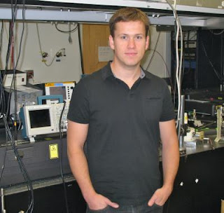
Caption: This is William Koehl. Credit: George Foulsham, Office of Public Affairs, UCSB, Usage Restrictions: None. | "We are looking for the beauty and utility in imperfection, rather than struggling to bring about perfect order," said Awschalom, "and to use these defects as the basis for a future quantum technology."
Most crystal imperfections do not possess these properties, which are intimately tied to the atomic structure of a defect and the electronic characteristics of its semiconductor host, explained Awschalom. In fact, before this research, the only system known to possess these same characteristics was a flaw in diamond known as the nitrogen-vacancy center.
The diamond nitrogen-vacancy center is renowned for its ability to function as a qubit at room temperature, while many other quantum states of matter require an extremely cold temperature, near absolute zero. However, this center exists in a material that is difficult to grow and challenging to manufacture into integrated circuits.
In contrast, high-quality crystals of silicon carbide, multiple inches in diameter, are commonly produced for commercial purposes. They can be readily fashioned into a multitude of intricate electronic, optoelectronic, and electromechanical devices. In addition, the defects studied by Awschalom and his group are addressed using infrared light that is close in energy to the light used widely throughout modern telecommunications networks. And while several distinct defect types were studied at a range of temperatures, two of them were capable of room temperature operation, just like the diamond nitrogen-vacancy center.
The combination of these features makes silicon carbide, with its defects, an attractive candidate for future work seeking to integrate quantum mechanical objects with sophisticated electronic and optical circuitry, according to the researchers. This research fits within a wider effort at UCSB to engineer quantum devices by fostering collaboration between the fields of materials science and quantum physics.
While defects in silicon carbide may offer many technologically attractive qualities, an immense number of defects in other semiconductors are still left to be explored. |
"Our dream is to make quantum mechanics fully engineerable," said William Koehl, lead author and a graduate student in the Awschalom lab. "Much like a civil engineer is able to design a bridge based on factors such as load capacity and length span, we'd like to see a day when there are quantum engineers who can design a quantum electronic device based on specifications such as degree of quantum entanglement and quality of interaction with the surrounding environment." ###
Contact: Gail Gallessich
gail.g@ia.ucsb.edu 805-893-7220
University of California - Santa Barbara


No comments:
Post a Comment