Team controls conduction, surface states in topological insulator nanoribbons
In recent years, topological insulators have become one of the hottest topics in physics. These new materials act as both insulators and conductors, with their interior preventing the flow of electrical currents while their edges or surfaces allow the movement of a charge.
Perhaps most importantly, the surfaces of topological insulators enable the transport of spin-polarized electrons while preventing the "scattering" typically associated with power consumption, in which electrons deviate from their trajectory, resulting in dissipation.
Because of such characteristics, these materials hold great potential for use in future transistors, memory devices and magnetic sensors that are highly energy efficient and require less power.
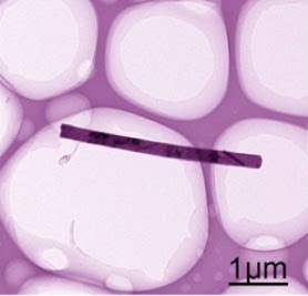
In a study published Feb. 13 in Nature Nanotechnology, researchers from UCLA's Henry Samueli School of Engineering and Applied Science and from the materials division of Australia's University of Queensland show the promise of surface-conduction channels in topological insulator nanoribbons made of bismuth telluride and demonstrate that surface states in these nanoribbons are "tunable" — able to be turned on and off depending on the position of the Fermi level.
"This research is very exciting because of the possibility to build nanodevices with a novel operating principle," said Wang, who is also associate director of the California NanoSystems Institute (CNSI) at UCLA. "Very similar to the development of graphene, the topological insulators could be made into high-speed transistors and ultra–high-sensitivity sensors."
The new findings shed light on the controllability of the surface spin states in topological insulator nanoribbons and demonstrate significant progress toward high surface electric conditions for practical device applications. The next step for Wang's team is to produce high-speed devices based on their discovery.
"The ideal scenario is to achieve 100 percent surface conduction with a complete insulating state in the bulk," Xiu said. "Based on the current work, we are targeting high-performance transistors with power consumption that is much less than the conventional complementary metal-oxide semiconductors (CMOS) technology used typically in today's electronics."
###
Study collaborators Jin Zou, a professor of materials engineering at the University of Queensland; Yong Wang, a Queensland International Fellow; and Zou's team at the division of materials at the University of Queensland contributed significantly to this work. A portion of the research was also done in Alexandros Shailos' lab at UCLA.
The study was funded by the Focus Center Research Program—Center on Functional Engineered Nano Architectonics (FENA) at UCLA Engineering; the U.S. Defense Advanced Research Projects Agency (DARPA); and the Australian Research Council. The research on topological insulators was pioneered by FENA's Shoucheng Zhang, a professor of physics at Stanford University.
The UCLA Henry Samueli School of Engineering and Applied Science, established in 1945, offers 28 academic and professional degree programs and has an enrollment of almost 5,000 students. The school's distinguished faculty are leading research to address many of the critical challenges of the 21st century, including renewable energy, clean water, health care, wireless sensing and networking, and cyber-security. Ranked among the top 10 engineering schools at public universities nationwide, UCLA Engineering is home to seven multimillion-dollar interdisciplinary research centers in wireless sensor systems, nanoelectronics, nanomedicine, renewable energy, customized computing, and the smart grid, all funded by federal and private agencies.
For more news, visit the UCLA Newsroom and follow us on Twitter.
Contact: Wileen Wong Kromhout wwkromhout@support.ucla.edu 310-206-0540 University of California - Los Angeles


No comments:
Post a Comment