Saturday, April 28, 2012

First self-assembly of nanoparticles into device-ready materials

Scientists with the Lawrence Berkeley National Laboratory (Berkeley Lab) and the University of California (UC) Berkeley have directed the first self-assembly of nanoparticles into device-ready materials. Through a relatively easy and inexpensive technique based on blending nanoparticles with block co-polymer supramolecules, the researchers produced multiple-layers of thin films from highly ordered one-, two- and three-dimensional arrays of gold nanoparticles. Thin films such as these have potential applications for a wide range of fields, including computer memory storage, energy harvesting, energy storage, remote-sensing, catalysis, light management and the emerging new field of plasmonics.

“We’ve demonstrated a simple yet versatile supramolecular approach to control the 3-D spatial organization of nanoparticles with single particle precision over macroscopic distances in thin films,” says polymer scientist Ting Xu, who led this research. “While the thin gold films we made were wafer-sized, the technique can easily produce much larger films, and it can be used on nanoparticles of many other materials besides gold.”

Xu holds joint appointments with Berkeley Lab’s Materials Sciences Division and UC Berkeley’s Departments of Materials Sciences and Engineering, and Chemistry. She is the corresponding author of a paper describing this research in the journal Nano Letters titled “Nanoparticle Assemblies in Thin Films of Supramolecular Nanocomposites.” Co-authoring the paper were Joseph Kao, Peter Bai, Vivian Chuang, Zhang Jiang and Peter Ercius.

Nanoparticles can be thought of as artificial atoms with unique optical, electrical and mechanical properties. If nanoparticles can be coaxed into routinely assembling themselves into complex structures and hierarchical patterns, similar to what nature does with proteins, devices a thousand times smaller than those of today’s microtechnologies could be mass-produced.


Berkeley Lab researchers have developed a relatively simple and inexpensive technique for directing the self-assembly of nanoparticles into device-ready thin films with microdomains of lamellar (left) or cylindrical morphologies. (courtesy of Ting Xu group)

Peter Bai, Joseph Kao and Ting Xu

From left Peter Bai, Joseph Kao and Ting Xu incorporated gold nanoparticles into solutions of block co-polymer supramolecules to form multiple-layers of self-assembled thin films. (Photo by Roy Kaltschmidt, Berkeley Lab)
Xu and her research group have been advancing towards this goal for the past decade. In a study earlier this year, they were able to induce rod-shaped semiconductor nanocrystals to self-assemble into one-, two- and even three-dimensional macroscopic structures. With this latest application of their methods to thin films, they have moved into the realm of material forms that are required for device fabrication and are well-suited for scalable nanomanufacturing.

“This is the first time that 2-D nanoparticle assembly, similar to those obtained using DNA linkers and controlled solvent evaporation, can be clearly achieved in multi-layers in supramolecule-based nanocomposite thin films,” Xu says. “Our supramolecular approach does not require chemical modification to any of the components in the composite system and, in addition to providing a means of building nanoparticle-based devices, should also provide a powerful platform for studying nanoparticle structure-property correlations.”

The technique developed by Xu and her colleagues uses solutions of block co-polymer supramolecules to direct the self-assembly of nanoparticles. A supramolecule is a group of molecules that act as a single molecule able to perform a specific set of functions. Block copolymers are long sequences or “blocks” of one type of monomer bound to blocks of another type of monomer that have an innate ability to self-assemble into well-defined arrays of nano-sized structures over macroscopic distances.

“Block copolymer supramolecules self-assemble and form a wide range of morphologies that feature microdomains typically a few to tens of nanometers in size,” Xu says. “As their size is comparable to that of nanoparticles, the microdomains of block copolymer supramolecules provide an ideal structural framework for the co-self-assembly of nanoparticles.”

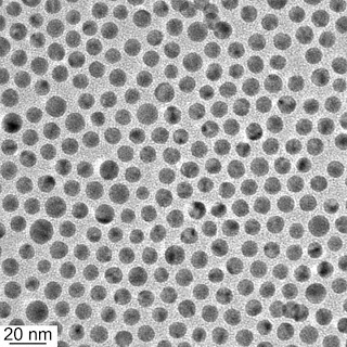
In this latest study, Xu and her colleagues incorporated gold nanoparticles into solutions of block co-polymer supramolecules to form films that ranged in thickness between 100 to 200 nanometers. The nanocomposite films featured microdomains in one of two common morphologies – lamellar or cylindrical. For the lamellar microdomains, the nanoparticles formed hexagonally-packed 2-D sheets that were stacked into multiple layers parallel to the surface. For the cylindrical microdomains, the nanoparticles formed 1-D chains (single particle width) that were packed into distorted hexagonal lattices in parallel orientation with the surface.

“Upon incorporation of nanoparticles, the block co-polymer supramolecules experience conformational changes, resulting in entropy that determines the placement and distribution of the nanoparticles, as well as the overall morphology of the nanocomposite thin films,” Xu says. “Our results indicate that it should be possible to generate highly-ordered lattices of nanoparticles within block co-polymer microdomains and obtain 3-D hierarchical assemblies of nanoparticles with precise structural control.”

The inter-particle distance between gold nanoparticles in the 1-D chains and the 2-D sheets was 8 to 10 nanometers, which raises intriguing possibilities with regards to plasmonics, the phenomenon by which a beam of light is confined in ultra-cramped spaces. Plasmonic technology holds great promise for superfast computers and optical microscopy, among other applications. However, a major challenge for developing plasmonics has been the difficulty of fabricating metamaterials with noble metal nanoparticles such as gold.

“Our gold thin films display strong plasmonic coupling along the inter-particle spacing in the 1-D chains and 2-D sheets respectively,” Xu says. “We should therefore be able to use these films to investigate unique plasmonic properties for next-generation electronic and photonic devices. Our supramolecular technique might also be used to fabricate plasmonic metamaterials.”

This research was supported by the U.S. Department of Energy Office of Science.

# # #

Lawrence Berkeley National Laboratory addresses the world’s most urgent scientific challenges by advancing sustainable energy, protecting human health, creating new materials, and revealing the origin and fate of the universe. Founded in 1931, Berkeley Lab’s scientific expertise has been recognized with 13 Nobel prizes. The University of California manages Berkeley Lab for the U.S. Department of Energy’s Office of Science. For more, visit www.lbl.gov.

Contact: Lynn Yarris lcyarris@lbl.gov 510-486-5375 DOE/Lawrence Berkeley National Laboratory

Wednesday, April 25, 2012

3D modulation-doping strategy

With new design, bulk semiconductor proves it can take the heat. Thin-film process boosts bulk alloy's thermoelectric performance.

CHESTNUT HILL, MA (April 25, 2012) – The intense interest in harvesting energy from heat sources has led to a renewed push to discover materials that can more efficiently convert heat into electricity. Some researchers are finding those gains by re-designing materials scientists have been working with for years.

A team of Boston College and MIT researchers report developing a novel, nanotech design that boosts the thermoelectric performance of a bulk alloy semiconductor by 30 to 40 percent above its previously achieved figure of merit, the measuring stick of conversion efficiency in thermoelectrics.

The alloy in question, Silicon Germanium, has been valued for its performance in high-temperature thermoelectric applications, including its use in radioisotope thermoelectric generators on NASA flight missions. But broader applications have been limited because of its low thermoelectric performance and the high cost of Germanium.

Boston College Professor of Physics Zhifeng Ren and graduate researcher Bo Yu, and MIT Professors Gang Chen and Mildred S. Dresselhause and post-doctoral researcher Mona Zebarjadi, report in the journal Nano Letters that altering the design of bulk SiGe with a process borrowed from the thin-film semiconductor industry helped produce a more than 50 percent increase in electrical conductivity.

3D Modulation-Doping Boosts Performance of Alloy Semiconductor SiGe

Caption: While long valued for high-temperature applications, the bulk alloy semiconductor SiGe hasn't lent itself to broader adoption because of its low thermoelectric performance and the high cost of Germanium. A novel nanotechnology design created by researchers from Boston College and MIT has shown a 30 to 40 percent increase in thermoelectric performance and reduced the amount of costly Germanium.

Credit: Nano Letters. Usage Restrictions: None.
The process, known as a 3D modulation-doping strategy, succeeded in creating a solid-state device that achieved a simultaneous reduction in the thermal conductivity, which combined with conductivity gains to provide a high figure of merit value of ~1.3 at 900 °C.

"To improve a material's figure of merit is extremely challenging because all the internal parameters are closely related to each other," said Yu. "Once you change one factor, the others may most likely change, leading to no net improvement. As a result, a more popular trend in this field of study is to look into new opportunities, or new material systems. Our study proved that opportunities are still there for the existing materials, if one could work smartly enough to find some alternative material designs."

Ren pointed out that the performance gains the team reported compete with the state-of-the-art n-type SiGe alloy materials, with a crucial difference that the team's design requires the use of 30 percent less Germanium, which poses a challenge to energy research because of its high cost. Lowering costs is crucial to new clean energy technologies, he noted.

"Using 30 percent less Germanium is a significant advantage to cut down the fabrication costs," said Ren. "We want all the materials we are studying in the group to help remove cost barriers. This is one of our goals for everyday research."

The collaboration between Ren and MIT's Chen has produced several breakthroughs in thermoelectric science, particularly in controlling phonon transport in bulk thermoelectric composite materials. The team's research is funded by the Solid State Solar Thermal Energy Conversion Center.

###

The 3STEC Center is part of the U.S. Department of Energy's Energy Frontier Research Center program, which is aimed at advancing fundamental science and developing materials to harness heat from the sun and convert the heat into electricity via solid-state thermoelectric and thermophotovoltaic technologies.

Contact: Ed Hayward ed.hayward@bc.edu 617-552-4826 Boston College

Monday, April 23, 2012

Effects of Chemical Bonding on Heat Transport Across Interfaces

CHAMPAIGN, Ill. — Through a combination of atomic-scale materials design and ultrafast measurements, researchers at the University of Illinois have revealed new insights about how heat flows across an interface between two materials.

The researchers demonstrated that a single layer of atoms can disrupt or enhance heat flow across an interface. Their results are published this week in Nature Materials.

Improved control of heat exchange is a key element to enhancing the performance of current technologies such as integrated circuits and combustion engines as well as emerging technologies such as thermoelectric devices, which harvest renewable energy from waste heat. However, achieving control is hampered by an incomplete understanding of how heat is conducted through and between materials.

"Heat travels through electrically insulating material via 'phonons,' which are collective vibrations of atoms that travel like waves through a material," said David Cahill, a Willett Professor and the head of materials science and engineering at Illinois and co-author of the paper. "Compared to our knowledge of how electricity and light travel through materials, scientists' knowledge of heat flow is rather rudimentary."

One reason such knowledge remains elusive is the difficulty of accurately measuring temperatures, especially at small-length scales and over short time periods – the parameters that many micro and nano devices operate under.

Over the past decade, Cahill's group has refined a measurement technique using very short laser pulses, lasting only one trillionth of a second, to probe heat flow accurately with nanometer-depth resolution. Cahill teamed up with Paul Braun, the Racheff Professor of Materials Science and Engineering at the U. of I. and a leader in nanoscale materials synthesis, to apply the technique to understanding how atomic-scale features affect heat transport.

"These experiments used a 'molecular sandwich' that allowed us to manipulate and study the effect that chemistry at the interface has on heat flow, at an atomic scale," Braun said.


Caption: Through atomic-scale manipulation, researchers at the University of Illinois have demonstrated that a single layer of atoms can disrupt or enhance heat flow across an interface.

Credit: Mark Losego. Usage Restrictions: None.
The researchers assembled their molecular sandwich by first depositing a single layer of molecules on a quartz surface. Next, through a technique known as transfer-printing, they placed a very thin gold film on top of these molecules. Then they applied a heat pulse to the gold layer and measured how it traveled through the sandwich to the quartz at the bottom.

By adjusting just the composition of the molecules in contact with the gold layer, the group observed a change in heat transfer depending on how strongly the molecule bonded to the gold. They demonstrated that stronger bonding produced a twofold increase in heat flow.

"This variation in heat flow could be much greater in other systems," said Mark Losego, who led this research effort as a postdoctoral scholar at Illinois and is now a research professor at North Carolina State University. "If the vibrational modes for the two solids were more similar, we could expect changes of up to a factor of 10 or more."

The researchers also used their ability to systematically adjust the interfacial chemistry to dial-in a heat flow value between the two extremes, verifying the ability to use this knowledge to design materials systems with desired thermal transport properties.

"We've basically shown that changing even a single layer of atoms at the interface between two materials significantly impacts heat flow across that interface," said Losego.

Scientifically, this work opens up new avenues of research. The Illinois group is already working toward a deeper fundamental understanding of heat transfer by refining measurement methods for quantifying interfacial bonding stiffness, as well as investigating temperature dependence, which will reveal a better fundamental picture of how the changes in interface chemistry are disrupting or enhancing the flow of heat across the interface.

"For many years, the physical models for heat flow between two materials have ignored the atomic-level features of an interface," Cahill said. "Now these theories need to be refined. The experimental methods developed here will help quantify the extent to which interfacial structural features contribute to heat flow and will be used to validate these new theories."

Braun and Cahill are affiliated with the Frederick Seitz Materials Research Laboratory at the U. of I. Braun is also affiliated with the department of chemistry and the Beckman Institute for Advanced Science and Technology. The Air Force Office of Scientific Research supported this work.

Contact: Liz Ahlberg eahlberg@illinois.edu 217-244-1073 University of Illinois at Urbana-Champaign

Saturday, April 21, 2012

VIDEO showing the growth of platinum nanocrystals at the atomic-scale in real-time

They won’t be coming soon to a multiplex near you, but movies showing the growth of platinum nanocrystals at the atomic-scale in real-time have blockbuster potential. A team of scientists with the Lawrence Berkeley National Laboratory (Berkeley Lab) and the University of California (UC) Berkeley has developed a technique for encapsulating liquids of nanocrystals between layers of graphene so that chemical reactions in the liquids can be imaged with an electron microscope. With this technique, movies can be made that provide unprecedented direct observations of physical, chemical and biological phenomena that take place in liquids on the nanometer scale.

“Watching real-time chemical reactions in liquids at the atomic-scale is a dream for chemists and physicists,” says Jungwon Park, a member of the team who holds joint appointments with Berkeley Lab’s Materials Sciences Division and UC Berkeley’s chemistry department. “Using our new graphene liquid cell, we’re able to capture a small amount of liquid sample under a high vacuum condition for taking real-time movies of nanoparticle growth reactions. Since graphene is chemically inert and extremely thin, our liquid cell provides realistic sample conditions for achieving high resolution and contrast.”

Park was the lead author, along with Jong Min Yuk, of a paper in the journal Science that describes this research titled “High-Resolution EM of Colloidal Nanocrystal Growth Using Graphene Liquid Cells.” The research was done as a collaboration between the research groups of Paul Alivisatos, director of Berkeley Lab and UC Berkeley’s Larry and Diane Bock Professor of Nanotechnology, and Alex Zettl, who holds joint appointments with Berkeley Lab’s Materials Sciences Division and UC Berkeley’s Physics Department where he directs the Center of Integrated Nanomechanical Systems. Both are corresponding authors of the Science paper along with Jeong Yong Lee of Korea’s Advanced Institute of Science and Technology (KAIST). Other authors were Peter Ercius, Kwanpyo Kim, Daniel Hellebusch and Michael Crommie.


In the graphene liquid cell, opposing graphene sheets form a sealed liquid nanoscale reaction chamber that is transparent to an electron microscope beam. The cell allows nanocrystal growth, dynamics and coalescence to be captured in real time at atomic resolution via a transmission electron microscope.

In using a beam of electrons rather than a beam of light for illumination and magnification, electron microscopes can “see” objects hundreds and even thousands of times smaller than what can be resolved with an optical microscope. However, electron microscopes can only operate in a high vacuum as molecules in the air disrupt the electron beam. Since liquids evaporate in high vacuum, liquid samples must be hermetically sealed in special solid containers – called cells – with a viewing window before they can be imaged in an electron microscope. Until now, such liquid cells have featured viewing windows made from silicon nitride or silicon oxide. While this has permitted studies of some nanoscale phenomena in liquids, the silicon-based cell windows are too thick to allow strong penetration by the electron beam and this has limited resolution to only a few nanometers. In addition to not allowing true atomic-resolution, the thick silicon-based cell windows also appear to perturb the natural state of the liquid or sample suspended in the liquid.


“Graphene is single carbon atom in thickness, making it one of the thinnest known membranes,” says Park, a member of the Alivisatos’ research group. “It does not scatter the electron beam but lets it pass through. Furthermore, graphene is also very strong and impermeable, as well as being chemically non-reactive, and this helps protects the sample in the liquid cell from the high-energy beam of an electron microscope.”

To make their graphene liquid cell, the Alivisatos-Zettl collaboration encapsulated a platinum growth solution between two laminated graphene layers that were suspended over holes in a conventional transmission electron microscope (TEM) grid. The graphene was grown on a copper foil substrate via chemical vapor deposition and then directly transferred onto a gold TEM mesh with a perforated amorphous carbon support. The platinum growth solution was pipetted directly atop two graphene-coated TEM grids facing in opposite directions. “Upon wetting the system, the solution wicks between the graphene and amorphous carbon layers, allowing one of the graphene sheets to detach from its associated TEM grid,” says co-author Kim, a member of the Zettl research group. “Because the van derWaals interaction between graphene sheets is relatively strong, liquid droplets ranging in thickness from six to 200 nanometers can be securely trapped in a pocket or blister between the graphene sheets.”

To test their graphene liquid cells, the collaborators used the world’s most powerful electron microscope, the TEAM I at the National Center for Electron Microscopy (NCEM), which is housed at Berkeley Lab. TEAM stands for Transmission Electron Aberration-corrected Microscope and the TEAM I instrument is capable of producing images with a half-angstrom resolution, which is less than the diameter of a single hydrogen atom. With TEAM I and their new graphene liquid cells, the Alivisatos-Zettl collaboration was able to directly observe at the highest resolution possible to date and with minimal sample perturbation, the growth of nanocrystals of platinum, one of the best metal catalysts in use today.

“Direct atomic-resolution imaging allowed us to visualize critical steps in the platinum nanocrystal growth process, including a host of previously unexpected phenomena, such as site-selective coalescence, structural reshaping after coalescence, and surface faceting,” says Park.

Three years ago, Park and Alivisatos were part of a team that used another TEM at NCEM and liquid cells featuring silicon nitride windows to record the first ever images of colloidal platinum nanocrystals growing in solution at subnanometer resolution. Their results showed that while some crystals in solution grew steadily in size via classical nucleation and aggregation – meaning molecules collide and join together – others grew in fits and spurts, driven by “coalescence events,” in which small crystals randomly collide and fuse together into larger crystals. Despite their distinctly different growth trajectories, these two processes ultimately yielded nanocrystals of approximately the same size and shape.

“In that earlier study, however, we lacked the resolution to fully understand how these nanoparticles merge and reorganize their shape in the coalescence growth trajectory,” Park says. “With the graphene liquid cells we used in this study, we were able to resolve the oriented coalescence along a specific crystal direction and see how they reorganized their overall structure into a final shape.” With the graphene liquid cells and the greater resolution of TEAM I, the Alivisatos-Zettl collaboration was able to observe that most coalescence events proceed along the same crystallographic direction – the {111} plane of the crystal. This points to a specific nanocrystal orientation for coalescence not seen before in metal nanoparticles.

“We were able to resolve atomistic arrangement at the moment two of the platinum nanoparticles merged and visualize oriented attachment, a phenomenon known to be one the of major growth mechanisms of anisotropic particles,” Park says. “This oriented coalescence could be one of the formation mechanisms behind another phenomenon we observed, twin boundaries, which occurs when nanoparticles merge together along the same {111} direction but on a mirror plane in the crystal.”

In the future, the collaborators plan to use their graphene liquid cells to study the growth of many different types of nanoparticles, including metals, semiconductors and other useful materials. The graphene cells could also be applied to biomaterials, such as DNA and proteins, which exist naturally in solution.

“The one atom thick graphene membranes are ideal for liquid encapsulation,” says co-author Ercius, the NCEM staff member who ran the TEAM I microscope for this study. “When combined with the aberration corrected imaging of TEAM I, we can reach the ultimate in image contrast and resolution for in-situ liquid experiments. The graphene liquid cell technique could be easily applied to other electron microscopes and I think it will become instrumental in answering questions regarding the synthesis of materials in liquids at the atomic scale.”

This work was supported by the U.S. Department of Energy’s Office of Science, and in part through the National Research Foundation of Korea.

# # #

Lawrence Berkeley National Laboratory addresses the world’s most urgent scientific challenges by advancing sustainable energy, protecting human health, creating new materials, and revealing the origin and fate of the universe. Founded in 1931, Berkeley Lab’s scientific expertise has been recognized with 13 Nobel prizes. The University of California manages Berkeley Lab for the U.S. Department of Energy’s Office of Science. For more, visit www.lbl.gov.

Contact: Lynn Yarris lcyarris@lbl.gov 510-486-5375 DOE/Lawrence Berkeley National Laboratory

Tuesday, April 17, 2012

Flexible Nanocrystal-Coated Glass Fibers for High-Performance Thermoelectric Energy Harvesting

Flexible Nanocrystal-Coated Glass Fibers for High-Performance Thermoelectric Energy Harvesting

WEST LAFAYETTE, Ind. – Researchers are developing a technique that uses nanotechnology to harvest energy from hot pipes or engine components to potentially recover energy wasted in factories, power plants and cars.

"The ugly truth is that 58 percent of the energy generated in the United States is wasted as heat," said Yue Wu, a Purdue University assistant professor of chemical engineering. "If we could get just 10 percent back that would allow us to reduce energy consumption and power plant emissions considerably."

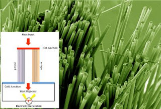
Researchers have coated glass fibers with a new "thermoelectric" material they developed. When thermoelectric materials are heated on one side electrons flow to the cooler side, generating an electrical current.

Coated fibers also could be used to create a solid-state cooling technology that does not require compressors and chemical refrigerants. The fibers might be woven into a fabric to make cooling garments.

The glass fibers are dipped in a solution containing nanocrystals of lead telluride and then exposed to heat in a process called annealing to fuse the crystals together.

Such fibers could be wrapped around industrial pipes in factories and power plants, as well as on car engines and automotive exhaust systems, to recapture much of the wasted energy. The "energy harvesting" technology might dramatically reduce how much heat is lost, Wu said.

Glass Fibers with Diagram

Caption: This image shows glass fibers coated with a thermoelectric material that generates electrical current when exposed to heat. The technology might be used to harvest energy from hot pipes or engine components, possibly representing a way to recover energy wasted in factories, power plants and cars.

Credit: Purdue University photo/Scott W. Finefrock. Usage Restrictions: None.
Findings were detailed in a research paper appearing last month in the journal Nano Letters. The paper was written by Daxin Liang, a former Purdue exchange student from Jilin University in China; Purdue graduate students Scott Finefrock and Haoran Yang; and Wu.

Today's high-performance thermoelectric materials are brittle, and the devices are formed from large discs or blocks.

"This sort of manufacturing method requires using a lot of material," Wu said.

The new flexible devices would conform to the irregular shapes of engines and exhaust pipes while using a small fraction of the material required for conventional thermoelectric devices.

"This approach yields the same level of performance as conventional thermoelectric materials but it requires the use of much less material, which leads to lower cost and is practical for mass production," Wu said.

The new approach promises a method that can be scaled up to industrial processes, making mass production feasible.

"We've demonstrated a material composed mostly of glass with only a 300-nanometer-thick coating of lead telluride," Finefrock said. "So while today's thermoelectric devices require large amounts of the expensive element tellurium, our material contains only 5 percent tellurium. We envision mass production manufacturing for coating the fibers quickly in a reel-to-reel process."

In addition to generating electricity when exposed to heat, the materials also can be operated in a reverse manner: Applying an electrical current causes it to absorb heat, representing a possible solid-state air-conditioning method. Such fibers might one day be woven into cooling garments or used in other cooling technologies.

The researchers have shown that the material has a promising thermoelectric efficiency, which is gauged using a formula to determine a measurement unit called ZT. A key part of the formula is the "Seebeck coefficient," named for 19th century German physicist Thomas Seebeck, who discovered the thermoelectric effect.

ZT is defined by the Seebeck coefficient, along with the electrical and thermal conductivity of the material and other factors. Having a low thermal conductivity, a high Seebeck coefficient and electrical conductivity results in a high ZT number.

"It's hard to optimize all of these three parameters simultaneously because if you increase electrical conductivity, and thermal conductivity goes up, the Seebeck coefficient drops," Wu said.

Most thermoelectric materials in commercial use have a ZT of 1 or below. However, nanostructured materials might be used to reduce thermal conductivity and increase the ZT number.

The Purdue researchers have used the ZT number to calculate the maximum efficiency that is theoretically possible with a material.

"We analyze the material abundance, the cost, toxicity and performance, and we established a single parameter called the efficiency ratio," Wu said.

Although high-performance thermoelectric materials have been developed, the materials are not practical for widespread industrial applications.

"Today's higher performance ones have a complicated composition, making them expensive and hard to manufacture," Wu said. "Also, they contain toxic materials, like antimony, which restricts thermoelectric research."

The nanocrystals are a critical ingredient, in part because the interfaces between the tiny crystals serve to suppress the vibration of the crystal lattice structure, reducing thermal conductivity. The materials could be exhibiting "quantum confinement," in which the structures are so tiny they behave nearly like individual atoms.

"This means that, as electrons carry heat through the structures, the average voltage of those heat-carrying electrons is higher than it would be in larger structures," Finefrock said. "Since you have higher-voltage electrons, you can generate more power."

This confinement can raise the ZT number.

A U.S. patent application has been filed for the fiber-coating concept.

Future work could focus on higher temperature annealing to improve efficiency, and the researchers also are exploring a different method to eliminate annealing altogether, which might make it possible to coat polymer fibers instead of glass.

"Polymers could be weaved into a wearable device that could be a cooling garment," Wu said.

The researchers also may work toward coating the glass fibers with a polymer to improve the resilience of the thermoelectric material, which tends to develop small cracks when the fibers are bent at sharp angles.

Researchers demonstrated the concept with an experiment using a system containing tubes of differing diameters nested inside a larger tube. Warm water flows through a central tube and cooler water flows through an outer tube, with a layer of thermoelectric material between the two.

The Purdue researchers also are exploring other materials instead of lead and tellurium, which are toxic, and preliminary findings suggest these new materials are capable of a high ZT value.

"Of course, the fact that our process uses such a small quantity of material – a layer only 300 nanometers thick – minimizes the toxicity issue," Wu said. "However, we also are concentrating on materials that are non-toxic and abundant."

###

The work has been funded by the National Science Foundation and U.S. Department of Energy.

Contact: Emil Venere venere@purdue.edu 765-494-3470 Purdue University

Sunday, April 15, 2012

Gold and copper nanoparticles form hybrid to catalyze carbon dioxide reduction

CAMBRIDGE, Mass. — Copper — the stuff of pennies and tea kettles — is also one of the few metals that can turn carbon dioxide into hydrocarbon fuels with relatively little energy. When fashioned into an electrode and stimulated with voltage, copper acts as a strong catalyst, setting off an electrochemical reaction with carbon dioxide that reduces the greenhouse gas to methane or methanol.

Various researchers around the world have studied copper’s potential as an energy-efficient means of recycling carbon dioxide emissions in powerplants: Instead of being released into the atmosphere, carbon dioxide would be circulated through a copper catalyst and turned into methane — which could then power the rest of the plant. Such a self-energizing system could vastly reduce greenhouse gas emissions from coal-fired and natural-gas-powered plants.

But copper is temperamental: easily oxidized, as when an old penny turns green. As a result, the metal is unstable, which can significantly slow its reaction with carbon dioxide and produce unwanted byproducts such as carbon monoxide and formic acid.

Now researchers at MIT have come up with a solution that may further reduce the energy needed for copper to convert carbon dioxide, while also making the metal much more stable. The group has engineered tiny nanoparticles of copper mixed with gold, which is resistant to corrosion and oxidation. The researchers observed that just a touch of gold makes copper much more stable. In experiments, they coated electrodes with the hybrid nanoparticles and found that much less energy was needed for these engineered nanoparticles to react with carbon dioxide, compared to nanoparticles of pure copper.

hybrid nanoparticles

Researchers have combined gold nanoparticles (in light red) with copper nanoparticles (in light green) to form hybrid nanoparticles (dark red), which they turned into powder (foreground) to catalyze carbon dioxide reduction. Photo: Zhichuan Xu.

hybrid nanoparticles

An electron microscopy image of hybrid gold/copper nanoparticles.
Image: Zhichuan Xu.
A paper detailing the results will appear in the journal Chemical Communications; the research was funded by the National Science Foundation. Co-author Kimberly Hamad-Schifferli of MIT says the findings point to a potentially energy-efficient means of reducing carbon dioxide emissions from powerplants.

“You normally have to put a lot of energy into converting carbon dioxide into something useful,” says Hamad-Schifferli, an associate professor of mechanical engineering and biological engineering. “We demonstrated hybrid copper-gold nanoparticles are much more stable, and have the potential to lower the energy you need for the reaction.”

Going small

The team chose to engineer particles at the nanoscale in order to “get more bang for their buck,” Hamad-Schifferli says: The smaller the particles, the larger the surface area available for interaction with carbon dioxide molecules. “You could have more sites for the CO2 to come and stick down and get turned into something else,” she says.

Hamad-Schifferli worked with Yang Shao-Horn, the Gail E. Kendall Associate Professor of Mechanical Engineering at MIT, postdoc Zhichuan Xu and Erica Lai ’14. The team settled on gold as a suitable metal to combine with copper mainly because of its known properties. (Researchers have previously combined gold and copper at much larger scales, noting that the combination prevented copper from oxidizing.)

To make the nanoparticles, Hamad-Schifferli and her colleagues mixed salts containing gold into a solution of copper salts. They heated the solution, creating nanoparticles that fused copper with gold.

Xu then put the nanoparticles through a series of reactions, turning the solution into a powder that was used to coat a small electrode.

To test the nanoparticles’ reactivity, Xu placed the electrode in a beaker of solution and bubbled carbon dioxide into it. He applied a small voltage to the electrode, and measured the resulting current in the solution. The team reasoned that the resulting current would indicate how efficiently the nanoparticles were reacting with the gas: If CO2 molecules were reacting with sites on the electrode — and then releasing to allow other CO2 molecules to react with the same sites — the current would appear as a certain potential was reached, indicating regular “turnover.” If the molecules monopolized sites on the electrode, the reaction would slow down, delaying the appearance of the current at the same potential.

The team ultimately found that the potential applied to reach a steady current was much smaller for hybrid copper-gold nanoparticles than for pure copper and gold — an indication that the amount of energy required to run the reaction was much lower than that required when using nanoparticles made of pure copper.

Going forward, Hamad-Schifferli says she hopes to look more closely at the structure of the gold-copper nanoparticles to find an optimal configuration for converting carbon dioxide. So far, the team has demonstrated the effectiveness of nanoparticles composed of one-third gold and two-thirds copper, as well as two-thirds gold and one-third copper.

Hamad-Schifferli acknowledges that coating industrial-scale electrodes partly with gold can get expensive. However, she says, the energy savings and the reuse potential for such electrodes may balance the initial costs.

“It’s a tradeoff,” Hamad-Schifferli says. “Gold is obviously more expensive than copper. But if it helps you get a product that’s more attractive like methane instead of carbon dioxide, and at a lower energy consumption, then it may be worth it. If you could reuse it over and over again, and the durability is higher because of the gold, that’s a check in the plus column.”

Written by: Jennifer Chu, MIT News Office

Contact: Caroline McCall, MIT Media Relations phone: 617-253-1682 cmccall5@mit.edu WEB: Massachusetts Institute of Technology

Thursday, April 12, 2012

light-harvesting nanoparticles convert laser energy into “plasmonic nanobubbles,” inject drugs and genetic payloads into cancer cells VIDEO

light-harvesting nanoparticles convert laser energy into “plasmonic nanobubbles,” inject drugs and genetic payloads into cancer cells. VIDEO

HOUSTON — Using light-harvesting nanoparticles to convert laser energy into “plasmonic nanobubbles,” researchers at Rice University, the University of Texas MD Anderson Cancer Center and Baylor College of Medicine (BCM) are developing new methods to inject drugs and genetic payloads directly into cancer cells. In tests on drug-resistant cancer cells, the researchers found that delivering chemotherapy drugs with nanobubbles was up to 30 times more deadly to cancer cells than traditional drug treatment and required less than one-tenth the clinical dose.

“We are delivering cancer drugs or other genetic cargo at the single-cell level,” said Rice’s Dmitri Lapotko, a biologist and physicist whose plasmonic nanobubble technique is the subject of four new peer-reviewed studies, including one due later this month in the journal Biomaterials and another published April 3 in the journal PLoS ONE. “By avoiding healthy cells and delivering the drugs directly inside cancer cells, we can simultaneously increase drug efficacy while lowering the dosage,” he said.

Delivering drugs and therapies selectively so they affect cancer cells but not healthy cells nearby is a major obstacle in drug delivery. Sorting cancer cells from healthy cells has been successful, but it is both time-consuming and expensive. Researchers have also used nanoparticles to target cancer cells, but nanoparticles can be taken up by healthy cells, so attaching drugs to the nanoparticles can also kill healthy cells.


Rice’s nanobubbles are not nanoparticles; rather, they are short-lived events. The nanobubbles are tiny pockets of air and water vapor that are created when laser light strikes a cluster of nanoparticles and is converted instantly into heat. The bubbles form just below the surface of cancer cells. As the bubbles expand and burst, they briefly open small holes in the surface of the cells and allow cancer drugs to rush inside. The same technique can be used to deliver gene therapies and other therapeutic payloads directly into cells.

CAPTION: Dmitri Lapotko CREDIT: Jeff Fitlow/Rice University

CAPTION: Dmitri Lapotko, CREDIT: Jeff Fitlow / Rice University

This method, which has yet to be tested in animals, will require more research before it might be ready for human testing, said Lapotko, faculty fellow in biochemistry and cell biology and in physics and astronomy at Rice.

The Biomaterials study due later this month reports selective genetic modification of human T-cells for the purpose of anti-cancer cell therapy. The paper, which is co-authored by Dr. Malcolm Brenner, professor of medicine and of pediatrics at BCM and director of BCM’s Center for Cell and Gene Therapy, found that the method “has the potential to revolutionize drug delivery and gene therapy in diverse applications.”

“The nanobubble injection mechanism is an entirely new approach for drug and gene delivery,” Brenner said. “It holds great promise for selectively targeting cancer cells that are mixed with healthy cells in the same culture.”

Lapotko’s plasmonic nanobubbles are generated when a pulse of laser light strikes a plasmon, a wave of electrons that sloshes back and forth across the surface of a metal nanoparticle. By matching the wavelength of the laser to that of the plasmon, and dialing in just the right amount of laser energy, Lapotko’s team can ensure that nanobubbles form only around clusters of nanoparticles in cancer cells.

Using the technique to get drugs through a cancer cell’s protective outer wall, or cell membrane, can dramatically improve the drug’s ability to kill the cancer cell, as shown by Lapotko and MD Anderson’s Xiangwei Wu in two recent studies, one in Biomaterials in February and another in Advanced Materials in March.

“Overcoming drug resistance represents one of the major challenges in cancer treatment,” said Wu. “Targeting plasmonic nanobubbles to cancer cells has the potential to enhance drug delivery and cancer-cell killing.”

To form the nanobubbles, the researchers must first get the gold nanoclusters inside the cancer cells. The scientists do this by tagging individual gold nanoparticles with an antibody that binds to the surface of the cancer cell. Cells ingest the gold nanoparticles and sequester them together in tiny pockets just below their surfaces.

While a few gold nanoparticles are taken up by healthy cells, the cancer cells take up far more, and the selectivity of the procedure owes to the fact that the minimum threshold of laser energy needed to form a nanobubble in a cancer cell is too low to form a nanobubble in a healthy cell

The research is funded by the National Institutes of Health and is described in the following recent papers:
###

Contact: Jade Boyd jadeboyd@rice.edu 713-348-6778 Rice University About Jade Boyd, Jade Boyd is science editor and associate director of news and media relations in Rice University's Office of Public Affairs.

VIDEO CREDIT:

Located on a 300-acre forested campus in Houston, Rice University is consistently ranked among the nation’s top 20 universities by U.S. News & World Report. Rice has highly respected schools of Architecture, Business, Continuing Studies, Engineering, Humanities, Music, Natural Sciences and Social Sciences and is known for its “unconventional wisdom.”

With 3,708 undergraduates and 2,374 graduate students, Rice’s undergraduate student-to-faculty ratio is 6-to-1. Its residential college system builds close-knit communities and lifelong friendships, just one reason why Rice has been ranked No. 1 for best quality of life multiple times by the Princeton Review and No. 4 for “best value” among private universities by Kiplinger’s Personal Finance.

Tuesday, April 10, 2012

Nanoparticle-based technique used to hunt for hidden pathogens

Researchers at the University of Central Florida have developed a novel technique that may give doctors a faster and more sensitive tool to detect pathogens associated with inflammatory bowel disease, including Crohn's disease.

The new nanoparticle-based technique also may be used for detection of other microbes that have challenged scientists for centuries because they hide deep in human tissue and are able to reprogram cells to successfully evade the immune system.

The microbes reappear years later and can cause serious health problems such as seen in tuberculosis cases. Current testing methods to find these hidden microbes exist, but require a long time to complete and often delay effective treatment for weeks or even months.

UCF Associate Professor J. Manuel Perez and Professor Saleh Naser and their research team have developed a method using nanoparticles coated with DNA markers specific to the elusive pathogens. The technique is effective and more accurate than current methods at picking up even small amounts of a pathogen. More important, it takes hours instead of weeks or months to deliver results, potentially giving doctors a quicker tool to help patients.

"Our new technique has surpassed traditional molecular and microbiological methods," said Naser, a professor at the UCF College of Medicine. "Without compromising specificity or sensitivity, the nano-method produced reliable and accurate results within hours compared to months."

The group's translational research works is published in today's edition of the journal PLOS One. dx.plos.org/10.1371/journal.pone

Dr. J. Manuel Perez, University of Central Florida

Dr. J. Manuel Perez, University of Central Florida. Caption: Dr. Perez works on nanotechnology at the University of Central Florida in Orlando.

Credit: UCF. Usage Restrictions: None.
The team created hybridizing magnetic relaxation nanosensors (hMRS) that can fish out and detect minuscule amounts of DNA from pathogens hiding within a patient's cells. The hair-thin hMRS are composed of a polymer-coated iron oxide nanoparticle and are chemically modified to specifically bind to a DNA marker that is unique to a particular pathogen.

When the hMRS bind to the pathogen's DNA, a magnetic resonance signal is detected, which is amplified by the water molecules that surround the nanoparticle. Then the researcher can read the change in the magnetic signature on a computer screen or portable electronic device, such as a smartphone, and determine whether the sample is infected with a particular pathogen.

The researchers used Mycobacterium avium spp. paratuberculosis (MAP), a pathogen that has been implicated in the cause of Johne's disease in cattle and Crohn's disease in humans, to test out their technique. They used a large number of blood and biopsy tissue samples from patients with Crohn's disease and meat samples from cattle with Johne's disease.

"It is all about giving medical professionals easy and reliable tools to better understand the spread of a disease, while helping people get treatment faster," said Perez, who works at UCF's Nanoscience Technology Center. "That's my goal. And that's where nanotechnology really has a lot to offer, particularly when the technology has been validated using clinical, food and environmental samples as is in our case."

The National Institute of General Medical Sciences (NIGMS), which is a part of the National Institutes of Health, and funded the research, said this kind of basic research can provide the foundation for medical breakthroughs.

"Just last year, Dr. Perez and his team unexpectedly discovered the DNA binding property of their magnetic nanosensors, and now they have shown that it may become the basis for a rapid, sensitive lab test for hard-to-measure bacteria and viruses in patient samples," said Janna Wehrle, Ph.D., of NIGMS. "This is a wonderful example of how quickly an advance can move from the research bench to meet an important clinical need."

###

Charalambos Kaittanis, who received his doctoral degree at UCF and worked as a postdoctoral Research Associate under Perez, has lead the experimental work in this study. Kaittanis is now a research fellow at Memorial Sloan-Kettering Cancer Center.

UCF Stands For Opportunity --The University of Central Florida is a metropolitan research university that ranks as the second largest in the nation with more than 58,000 students. UCF's first classes were offered in 1968. The university offers impressive academic and research environments that power the region's economic development. UCF's culture of opportunity is driven by our diversity, Orlando environment, history of entrepreneurship and our youth, relevance and energy. For more information visit news.ucf.edu

Contact: Zenaida Gonzalez Kotala zenaida.kotala@ucf.edu 407-823-6120 University of Central Florida

Sunday, April 08, 2012

Microfluidics-based microarray could radically change how and when cancer is diagnosed

McGill team develops new technology that can accurately measure protein biomarkers

One in eight women will be diagnosed with breast cancer during her lifetime. The earlier cancer is detected, the better the chance of successful treatment and long-term survival. However, early cancer diagnosis is still challenging as testing by mammography remains cumbersome, costly, and in many cases, cancer can only be detected at an advanced stage. A team based in the Dept. of Biomedical Engineering at McGill University’s Faculty of Medicine has developed a new microfluidics-based microarray that could one day radically change how and when cancer is diagnosed. Their findings are published in the April issue of the journal Molecular & Cellular Proteomics.

For years, scientists have worked to develop blood tests for cancer based on the presence of the Carcinoembryonic Antigen (CEA), a protein biomarker for cancer identified over 40 years ago by McGill’s Dr. Phil Gold. This biomarker, however, is also found in healthy people and its concentration varies from person to person depending on genetic background and lifestyle. As such, it has not been possible to establish a precise cut-off between healthy individuals and those with cancer.

“Attempts have been made to overcome this problem of person-to-person variability by seeking to establish a molecular ‘portrait’ of a person by measuring both the concentration of multiple proteins in the blood and identifying the signature molecules that, taken together, constitute a characteristic ‘fingerprint’ of cancer,” explains Dr. David Juncker, the team’s principal investigator. “However, no reliable set of biomarkers has been found, and no such test is available today. Our goal is to find a way around this.”

breast cancerDr. Mateu Pla-Roca, the study’s first author, along with members of Juncker’s team, began by analyzing the most commonly used existing technologies that measure multiple proteins in the blood and developing a model describing their vulnerabilities and limitations. Specifically, they discovered why the number of protein targets that can be measured simultaneously has been limited and why the accuracy and reproducibility of these tests have been so challenging to improve. Armed with a better understanding of these limitations, the team then developed a novel microfluidics-based microarray technology that circumvents these restrictions. Using this new approach, it then became possible to measure as many protein biomarkers as desired while minimizing the possibility of obtaining false results.

Juncker’s biomedical engineering group, together with oncology and bioinformatics teams from McGill’s Goodman Cancer Research Centre, then measured the profile of 32 proteins in the blood of 11 healthy controls and 17 individuals who had a particular subtype of breast cancer (estrogen receptor-positive). The researchers found that a subset of six of these 32 proteins could be used to establish a fingerprint for this cancer and classify each of the patients and healthy controls as having or not having breast cancer.

“While this study needs to be repeated with additional markers and a greater diversity of patients and cancer subsets before such a test can be applied to clinical diagnosis, these results nonetheless underscore the exciting potential of this new technology,” said Juncker.

Looking ahead, Juncker and his collaborators have set as their goal the development of a simple test that can be carried out in a physician’s office using a droplet of blood, thereby reducing dependence on mammography and minimizing attendant exposure to X-rays, discomfort and cost. His lab is currently developing a hand-held version of the test and is working on improving its sensitivity so as to be able to accurately detect breast cancer and ultimately, many other diseases, at the earliest possible stage.

This study was funded by the Canadian Institutes for Health Research (CIHR), Genome Canada; Génome Québec; The Canada Foundation for Innovation (CFI), The Natural Science and Engineering Research Council (NSERC); and the Banque de tissue et de données of the Réseau de la Recherches sur le cancer (RRCancer) of the Fonds de recherche en santé du Québec (FRSQ).

Contact: Chris Chipello Media Relations Office McGill University 514-398-4201 christopher.chipello@mcgill.ca April 5, 2012

Friday, April 06, 2012

Direct Observation of Nanoparticle Cancer Cell Nucleus Interactions

Tiny Hitchhikers Attack Cancer Cells. Gold nanostars first to deliver drug directly to cancer cell nucleus.

EVANSTON, Ill. --- Nanotechnology offers powerful new possibilities for targeted cancer therapies, but the design challenges are many. Northwestern University scientists now are the first to develop a simple but specialized nanoparticle that can deliver a drug directly to a cancer cell’s nucleus -- an important feature for effective treatment.

They also are the first to directly image at nanoscale dimensions how nanoparticles interact with a cancer cell’s nucleus.

“Our drug-loaded gold nanostars are tiny hitchhikers,” said Teri W. Odom, who led the study of human cervical and ovarian cancer cells. “They are attracted to a protein on the cancer cell’s surface that conveniently shuttles the nanostars to the cell’s nucleus. Then, on the nucleus’ doorstep, the nanostars release the drug, which continues into the nucleus to do its work.”

Odom is the Board of Lady Managers of the Columbian Exposition Professor of Chemistry in the Weinberg College of Arts and Sciences and a professor of materials science and engineering in the McCormick School of Engineering and Applied Science.

Using electron microscopy, Odom and her team found their drug-loaded nanoparticles dramatically change the shape of the cancer cell nucleus. What begins as a nice, smooth ellipsoid becomes an uneven shape with deep folds. They also discovered that this change in shape after drug release was connected to cells dying and the cell population becoming less viable -- both positive outcomes when dealing with cancer cells.

Teri W. Odom

Teri W. Odom
The results are published in the journal ACS Nano.

Since this initial research, the researchers have gone on to study effects of the drug-loaded gold nanostars on 12 other human cancer cell lines. The effect was much the same. “All cancer cells seem to respond similarly,” Odom said. “This suggests that the shuttling capabilities of the nucleolin protein for functionalized nanoparticles could be a general strategy for nuclear-targeted drug delivery.”

The nanoparticle is simple and cleverly designed. It is made of gold and shaped much like a star, with five to 10 points. (A nanostar is approximately 25 nanometers wide.) The large surface area allows the researchers to load a high concentration of drug molecules onto the nanostar. Less drug would be needed than current therapeutic approaches using free molecules because the drug is stabilized on the surface of the nanoparticle.

The drug used in the study is a single-stranded DNA aptamer called AS1411. Approximately 1,000 of these strands are attached to each nanostar’s surface.

The DNA aptamer serves two functions: it is attracted to and binds to nucleolin, a protein overexpressed in cancer cells and found on the cell surface (as well as within the cell). And when released from the nanostar, the DNA aptamer also acts as the drug itself.

Bound to the nucleolin, the drug-loaded gold nanostars take advantage of the protein’s role as a shuttle within the cell and hitchhike their way to the cell nucleus. The researchers then direct ultrafast pulses of light -- similar to that used in LASIK surgery -- at the cells. The pulsed light cleaves the bond attachments between the gold surface and the thiolated DNA aptamers, which then can enter the nucleus.

In addition to allowing a large amount of drug to be loaded, the nanostar’s shape also helps concentrate the light at the points, facilitating drug release in those areas. Drug release from nanoparticles is a difficult problem, Odom said, but with the gold nanostars the release occurs easily.

That the gold nanostar can deliver the drug without needing to pass through the nuclear membrane means the nanoparticle is not required to be a certain size, offering design flexibility. Also, the nanostars are made using a biocompatible synthesis, which is unusual for nanoparticles.

Odom envisions the drug-delivery method, once optimized, could be particularly useful in cases where tumors are fairly close to the skin’s surface, such as skin and some breast cancers. (The light source would be external to the body.) Surgeons removing cancerous tumors also might find the gold nanostars useful for eradicating any stray cancer cells in surrounding tissue.

The National Institutes of Health supported the research.

The title of the ACS Nano paper is “Direct Observation of Nanoparticle-Cancer Cell Nucleus Interactions.” In addition to Odom, other authors of the paper are Duncan Hieu M. Dam, Jung Heon Lee, Patrick N. Sisco, Dick T. Co, Ming Zhang and Michael R. Wasielewski, all from Northwestern University.

Contact: Megan Fellman fellman@northwestern.edu 847-491-3115 Northwestern University

Wednesday, April 04, 2012

Decoherence-protected quantum gates for a hybrid solid-state spin register

(Santa Barbara, Calif.) –– A protocol for controlling quantum information pioneered by researchers at UC Santa Barbara, the Kavli Institute of Nanoscience in Delft, the Netherlands, and the Ames Laboratory at Iowa State University could open the door to larger-scale, more accurate quantum computations. Their findings, in a paper titled "Decoherence-protected quantum gates for a hybrid solid-state spin register," are published in the current issue of the journal Nature.

"Although interactions between a quantum bit ('qubit') and its environment tend to corrupt the information it stores, it is possible to dynamically control qubits in a way that facilitates the execution of quantum information-processing algorithms while simultaneously protecting the qubits from environment-induced errors," said UCSB physicist David Awschalom. He and his group were responsible for developing the electron and nuclear spins used as the quantum bits –– the quantum version of the computer bit –– in their demonstration and for helping to analyze the results.

Awschalom is director of UCSB's Center for Spintronics & Quantum Computation, professor of physics, electrical and computer engineering, and the Peter J. Clarke Director of the California NanoSystems Institute.

Dynamical protection of quantum information is essential for quantum computing as the qubits used for information processing and storage are highly susceptible to errors induced by interactions with atoms in the qubits' environment. The scientists' previous research has shown that quantum information stored in qubits can be effectively protected through successive control operations (rotations) on a qubit that filter out these unwanted interactions. However, these control operations also filter out the interactions between qubits that are essential for the realization of logic gates for quantum information processing. Thus, until recently, quantum information stored in protected qubit states could not be used for quantum computations.

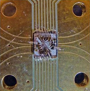
Quantum Circuit

Caption: The quantum circuit used in the demonstration is a 3mm x 3mm chip with a 1mm x 1mm diamond in the middle.

Credit: Delft University of Technology/UC Santa Barbara. Usage Restrictions: None.
The research team, which also included members from the University of Southern California, showed that by precisely synchronizing the rotations of an electron spin with the rotation of a nearby nuclear spin, they could realize dynamical protection of both qubits from the environment while maintaining the interactions between the two spins that are necessary for quantum information processing. As a proof of principle, the researchers demonstrated the high-fidelity execution of a quantum search algorithm using this two-qubit system. Quantum search algorithms, if executed on a larger number of qubits, could provide search results of certain databases considerably faster than search algorithms performed on a classical computer.

The results of this study point to greater possibilities for quantum computers that overcome, according to Awschalom, the perception that spin qubits in semiconductors, such as those used in this work, suffer from too strong of environmental interactions to be useful qubits.

These solid state spin systems also offer the added benefit of operating at room temperature, in contrast to other candidate qubit systems which operate at only at a fraction of a degree above absolute zero.

"This demonstration of performing a quantum algorithm at the subatomic level with single spins suggests a pathway to build increasingly complex quantum machines, using qubit control protocols that circumvent the expected limitations from real materials," said Awschalom.

###

Contact: Sonia Fernandez sonia.fernandez@ia.ucsb.edu 805-893-4765 University of California - Santa Barbara

Monday, April 02, 2012

Ground-breaking advances in our understanding of the changes that materials undergo when rapidly heated.

Collaboration between the University of Southampton and the University of Cambridge has made ground-breaking advances in our understanding of the changes that materials undergo when rapidly heated.

Using cutting edge equipment and specially designed MEM's sensors on loan from Mettler-Toledo, scientists from the University of Southampton's Optoelectronic Research Centre and the University of Cambridge's Department of Materials Science were able to probe the behaviour of phase change memory materials, the semiconductors that store information in the next generation of electronics, as they were heated at rates up to 10,000 degree C per second.

Insight and a detailed understanding of measurement results was provided by Professor Lindsay Greer, from the University of Cambridge's Department of Materials Science, whose analysis showed that crystal growth rates differed considerably from other materials such as glass and silicon and the behaviour of these materials on such rapid heating was not as expected.

The results, which are published this week in Nature Materials, show that crystal growth rates are much faster than we previously believed in these materials and that the growth behaviour is independent of the surroundings. While it is not surprising that properties of materials change significantly when they are shrunk to nanoscale dimensions, we now have a method of directly screening materials for improved memory performance; this means faster, smaller and less power hungry smart phones, ipods and computers are one step closer.

Behrad Gholipour, University of Southampton

Caption: Behrad Gholipour led the team that provided the phase change materials and deposited them as very thin films.

Credit: University of Southampton, Usage Restrictions: None.
Professor Dan Hewak from the University of Southampton, whose team, led by Behrad Gholipour, provided the phase change materials and deposited them as very thin films, comments:

"We have been studying novel glasses and phase change materials for two decades here at the Optoelectronics Research Centre. However, our understanding of what happens when these materials are heated, that is, their crystallization and melting behaviours, has been limited to heating rates of about 10 degrees C per minute using conventional thermal analysis. In reality, in the memory devices we fabricate, heating rates are millions of times faster and it is reasonable to expect that in order to improve these devices, an understanding of their properties at the same heating rates they will be used is needed."

Writing in the same issue of Nature Materials, Professors Matthias Wuttig and Martin Salinga at RWTH Aachen University in Germany explain why this breakthrough is so important: "Jiri Orava (Cambridge University) and colleagues now provide a completely new insight in our understanding of the fast transformations that occur in the materials that make up today's memory devices. Reading and writing of data in optical memory such as rewriteable compact discs (CD-RWs and DVDs) and emerging new electronic memory can take place at speeds of tens of nanoseconds but our understanding of what happens when these materials are heated is based on experiments where heating rates are much slower."

"Unravelling the mysteries of chocolate making, comprehending the formation of amethyst geodes, or producing advanced steels requires an understanding of the relevant crystallization phenomena."

###

Contact: Glenn Harris G.Harris@soton.ac.uk 44-023-805-93212 University of Southampton