Saturday, April 30, 2011

A new approach to producing nanocrystals with predictable shapes by utilizing surfactants

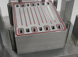
Currently, some 20 percent of the world's industrial production is based on catalysts — molecules that can quicken the pace of chemical reactions by factors of billions. Oil, pharmaceuticals, plastics and countless other products are made by catalysts.

Many are hoping to make current catalysts more efficient, resulting in less energy consumption and less pollution. Highly active and selective nanocatalysts, for example, can be used effectively in efforts to break down pollution, create hydrogen fuel cells, store hydrogen and synthesize fine chemicals. The challenge to date has been developing a method for producing nanocatalysts in a controlled, predictable way.

In a move in this direction, Yu Huang, an assistant professor of materials science and engineering at the UCLA Henry Samueli School of Engineering and Applied Science, and her research team have proposed and demonstrated a new approach to producing nanocrystals with predictable shapes by utilizing surfactants, biomolecules that can bind selectively to certain facets of the crystals' exposed surfaces.

Their new study can be found online in the journal Nature Chemistry.

Peptide directed nanocrystal synthesis

Peptide-directed nanocrystal synthesis
At the nanoscale, the physical and chemical properties of materials depend on the materials' size and shape. The ultimate goal has been to rationally engineer materials to achieve programmable structures and predictable properties, thereby producing the desired functions. Yet shaped nanocrystals are still generally synthesized by trial-and-error, using non-specific molecules as surfactants — a result of the inability to find appropriate molecules to control crystal formation.

Huang's team's innovative new work could change that, potentially leading to the ability to rationally produce nanocatalysts with desired shapes and, hence, catalytic properties.

"In our study, we were able to identify specific biomolecules — peptide sequences, in our case — which can recognize a desired crystal surface and produce nanocrystals exposed with a particular surface to control the shape," said Chin-Yi Chiu, a UCLA Engineering graduate student and lead author of the study.

"Facet-specific biomolecules can be used to direct the growth of nanocrystals, and most importantly, now we can do it in a predictable fashion," said Huang, senior author of the study. "This is still a first step, but we have overcome the challenges by finding the most specific and selective peptide sequences through a rational selection process."

Huang's team accomplished this by using a phage library that generated a pool of peptide sequences. The team was then able to identify the selectivity of peptide sequences on different crystal surfaces. The next step, the researchers say, is to figure out what exactly is happening on the interface and to be able to describe the characterizations of the interface.

"We don't know the molecular details yet — that's like the holy grail of molecular biomimetics," Huang said. "Take the catalyst, for example. If we can predict the synthesized catalyst for just one surface, it could have much more improved activity and selectivity. We are still in the initial phase of what we really want to do, which is to see whether or not we can eventually program the synthesis of material structures."

"It's always been a personal interest to learn from the natural evolutionary selection process and apply it to research," Chiu said. "It is especially satisfying to be able to engineer a rational selection process for nanoscale materials to create nanocrystals with desired shapes."

###

The study was funded by the U.S. Office of Naval Research; the U.S. Army Research Office, through the Presidential Early Career Award for Scientists and Engineers (PECASE); and a Sloan Research Fellowship.

The UCLA Henry Samueli School of Engineering and Applied Science, established in 1945, offers 28 academic and professional degree programs and has an enrollment of almost 5,000 students. The school's distinguished faculty are leading research to address many of the critical challenges of the 21st century, including renewable energy, clean water, health care, wireless sensing and networking, and cybersecurity. Ranked among the top 10 engineering schools at public universities nationwide, the school is home to seven multimillion-dollar interdisciplinary research centers in wireless sensor systems, nanoelectronics, nanomedicine, renewable energy, customized computing, and the smart grid, all funded by federal and private agencies.

Contact: Wileen Wong Kromhout wwkromhout@support.ucla.edu 310-206-0540 University of California - Los Angeles

Thursday, April 28, 2011

Alexander Balandin selected to receive the Pioneer of Nanotechnology Award for 2011

RIVERSIDE, Calif. (www.ucr.edu) -- A professor at the University of California, Riverside’s Bourns College of Engineering will receive an international award for his pioneering work in nanotechnology that could have far-reaching impacts on electronic devices.

Alexander Balandin, a professor of electrical engineering and founding chair of a campus-wide Materials Science and Engineering Program, was selected to receive the Pioneer of Nanotechnology Award for 2011, the Nanotechnology Council of IEEE, formerly known as The Institute for Electrical and Electronics Engineers, announced Friday.

He will receive the award and give a keynote talk at the organization’s conference in Portland, Oregon in mid-August. Only one university professor is selected for this award each year.

Balandin, a native of Russia who has been at UC Riverside since 1999, is the first professor in the University of California system to receive the award. Previous recipients of the award include distinguished professors from the University of Toronto, Yale University and the University of Michigan. Last year’s award recipient was internationally renowned scientist Phaedon Avouris from the IBM T.J. Watson Research Center in Yorktown Heights, NY.

Alexander Balandin“It’s really an honor, especially considering the people who have received this award before me,” Balandin said.

Reza Abbaschian, dean of the Bourns College of Engineering at UC Riverside, said the recognition is well-deserved.

“I predict it is one of many awards Alexander Balandin will earn in the years ahead,” Abbaschian said. “His ground-breaking research, contributions to his field and his leadership in developing our Materials Science and Engineering Program have been invaluable to our college, our students and the science and engineering community at-large."

The award recognizes individuals who by virtue of initiating new areas of research, development or engineering have had a significant and transformative impact on the field of nanotechnology.

Balandin is receiving the award for his “pioneering contributions to nanoscale phonon transport with applications in nanodevices, graphene devices, thermoelectric and thermal management of advanced electronics.”

“He is one of the leaders in the field and has done pioneering research that clearly can have major impacts on electronic devices,” said James Morris, a professor of electrical and computer engineering at Portland State University who chaired the committee that recommended Balandin receive the award.

Balandin is an internationally renowned expert in the area of advanced materials, nanostructures and nanodevices. He is a fellow of the Optical Society of America, the International Society for Optical Engineering and the American Association for Advancement of Science.

Since 1997, he has been developing the concept of nanoscale phonon engineering and its applications to heat removal from advanced electronic chips and renewable energy conversion. Phonons are quanta of crystal lattices vibrations in materials. They affect electrical resistance and determine thermal conductivity of semiconductor materials used in electronics.

In 2008, his research group made the important discovery of the extremely high intrinsic thermal conductivity of graphene and explained it theoretically. To perform the first measurements of heat conduction in graphene, Balandin invented an experimental optothermal technique based on Raman spectroscopy.

Balandin’s group has also demonstrated the first low-noise top-gate single-layer graphene transistor, graphene triple mode amplifier and phase detector, and carried out the first “graphene-like” mechanical exfoliation of thin films of a new class of materials - topological insulators.

IEEE is the world’s largest professional association dedicated to advancing technological innovation and excellence for the benefit of humanity. It has more than 400,000 members in more than 160 countries. The Nanotechnology Council consists of 21 IEEE member societies.

Contact: Sean Nealon sean.nealon@ucr.edu 951-827-1287 University of California - Riverside

Wednesday, April 27, 2011

A new biosensor microchip that could hold more than 100,000 magnetically sensitive nanosensors could speed up drug development markedly

A new biosensor microchip that could hold more than 100,000 magnetically sensitive nanosensors could speed up drug development markedly, Stanford researchers say. The nanosensors analyze how proteins bond – a critical step in drug development. The ultrasensitive sensors can simultaneously monitor thousands of times more proteins than existing technology, deliver results faster and assess the strength of the bonds.

Stanford researchers have developed a new biosensor microchip that could significantly speed up the process of drug development. The microchips, packed with highly sensitive "nanosensors," analyze how proteins bind to one another, a critical step for evaluating the effectiveness and possible side effects of a potential medication.

A single centimeter-sized array of the nanosensors can simultaneously and continuously monitor thousands of times more protein-binding events than any existing sensor. The new sensor is also able to detect interactions with greater sensitivity and deliver the results significantly faster than the present "gold standard" method.

"You can fit thousands, even tens of thousands, of different proteins of interest on the same chip and run the protein-binding experiments in one shot," said Shan Wang, a professor of materials science and engineering, and of electrical engineering, who led the research effort.

microchip with an array of 64 nanosensors

A microchip with an array of 64 nanosensors. The nanosensors appear as small dark dots in an 8 x 8 grid in the center of the illuminated part of the backlit microchip.
"In theory, in one test, you could look at a drug's affinity for every protein in the human body," said Richard Gaster, MD/PhD candidate in bioengineering and medicine, who is the first author of a paper describing the research that is in the current issue of Nature Nanotechnology, available online now.

The power of the nanosensor array lies in two advances. First, the use of magnetic nanotags attached to the protein being studied – such as a medication – greatly increases the sensitivity of the monitoring.

Second, an analytical model the researchers developed enables them to accurately predict the final outcome of an interaction based on only a few minutes of monitoring data. Current techniques typically monitor no more than four simultaneous interactions and the process can take hours.

"I think their technology has the potential to revolutionize how we do bioassays," said P.J. Utz, associate professor of medicine (immunology and rheumatology) at Stanford University Medical Center, who was not involved in the research.

Members of Wang's research group developed the magnetic nanosensor technology several years ago and demonstrated its sensitivity in experiments in which they showed that it could detect a cancer-associated protein biomarker in mouse blood at a thousandth of the concentration that commercially available techniques could detect. That research was described in a 2009 paper in Nature Medicine.

The researchers tailor the nanotags to attach to the particular protein being studied. When a nanotag-equipped protein binds with another protein that is attached to a nanosensor, the magnetic nanotag alters the ambient magnetic field around the nanosensor in a small but distinct way that is sensed by the detector.

"Let's say we are looking at a breast cancer drug," Gaster said. "The goal of the drug is to bind to the target protein on the breast cancer cells as strongly as possible. But we also want to know: How strongly does that drug aberrantly bind to other proteins in the body?"

To determine that, the researchers would put breast cancer proteins on the nanosensor array, along with proteins from the liver, lungs, kidneys and any other kind of tissue that they are concerned about. Then they would add the medication with its magnetic nanotags attached and see which proteins the drug binds with – and how strongly.

"We can see how strongly the drug binds to breast cancer cells and then also how strongly it binds to any other cells in the human body such as your liver, kidneys and brain," Gaster said. "So we can start to predict the adverse affects to this drug without ever putting it in a human patient."

It is the increased sensitivity to detection that comes with the magnetic nanotags that enables Gaster and Wang to determine not only when a bond forms, but also its strength.

"The rate at which a protein binds and releases, tells how strong the bond is," Gaster said. That can be an important factor with numerous medications.

"I am surprised at the sensitivity they achieved," Utz said. "They are detecting on the order of between 10 and 1,000 molecules and that to me is quite surprising."

The nanosensor is based on the same type of sensor used in computer hard drives, Wang said.

"Because our chip is completely based on existing microelectronics technology and procedures, the number of sensors per area is highly scalable with very little cost," he said.

Although the chips used in the work described in the Nature Nanotechnology paper had a little more than 1,000 sensors per square centimeter, Wang said it should be no problem to put tens of thousands of sensors on the same footprint.

"It can be scaled to over 100,000 sensors per centimeter, without even pushing the technology limits in microelectronics industry," he said.

Wang said he sees a bright future for increasingly powerful nanosensor arrays, as the technology infrastructure for making such nanosensor arrays is in place today.

"The next step is to marry this technology to a specific drug that is under development," Wang said. "That will be the really killer application of this technology."

Other Stanford researchers who participated in the research and are coauthors of the Nature Nanotechnology paper are Liang Xu and Shu-Jen Han, both of whom were graduate students in materials science and engineering at the time the research was done; Robert Wilson, senior scientist in materials science and engineering; and Drew Hall, graduate student in electrical engineering. Other coauthors are Drs. Sebastian Osterfeld and Heng Yu from MagArray Inc. in Sunnyvale. Osterfeld and Yu are former alumni of the Wang Group.

Funding for the research came from the National Cancer Institute, the National Science Foundation, the Defense Advanced Research Projects Agency, the Gates Foundation and National Semiconductor Corporation.

Contact: Louis Bergeron louisb3@stanford.edu 650-725-1944 Stanford University

Tuesday, April 26, 2011

Rare Physical Phenomenon at Low Temperatures and High Magnetic Fields Ferromagnetism plus Superconductivity

It actually seems impossible: Scientists from the Helmholtz-Zentrum Dresden-Rossendorf (HZDR) and the TU Dresden were able to verify with an intermetallic compound of bismuth and nickel that certain materials actually exhibit the two contrary properties of superconductivity and ferromagnetism at the same time. A phenomenon that had only been demonstrated around the globe on a small number of materials and which might provide highly interesting technological opportunities in future.

Just in time for the 100th anniversary to commemorate the discovery of superconductivity by the Dutch physicist Heike Kamerlingh Onnes on April 8, 1911, scientists from the Helmholtz-Zentrum Dresden-Rossendorf and the TU Dresden published their research results in the journal Physical Review B. Headed by Dr. Thomas Herrmannsdörfer, the team from the HZDR’s High Magnetic Field Laboratory (HLD) examined a material consisting of the elements bismuth and nickel (Bi3Ni) with a diameter of only a few nanometers – which is unique since it has not been achieved elsewhere so far. This was made possible through a new chemical synthesis procedure at low temperatures which had been developed at the TU Dresden under the leadership of Prof. Michael Ruck. The nano scale size and the special form of the intermetallic compound – namely, tiny fibers – caused the physical properties of the material, which is non-magnetic under normal conditions, to change so dramatically. This is a particularly impressive example of the excellent opportunities modern nanotechnology can provide today, emphasizes Dr. Thomas Herrmannsdörfer. “It’s really surprising to which extend the properties of a substance can vary if one manages to reduce their size to the nanometer scale.”

bundle of parallel-oriented Bi3Ni fibers which become both ferromagnetic and superconducting at low temperatures

Image from a scanning electron microscope showing a bundle of parallel-oriented Bi3Ni fibers which become both ferromagnetic and superconducting at low temperatures. Looking into such a fiber, one will discover an only few nanometer wide atomic lattice structure made out of bismuth (blue) and nickel atoms (green)
There are numerous materials which become superconducting at ultralow temperatures. However, this property competes with ferromagnetism which normally suppresses superconductivity. This does not happen with the analyzed compound: Here, the Dresden researchers discovered with their experiments in high magnetic fields and at ultralow temperatures that the nanostructured material exhibits completely different properties than larger-sized samples of the same material. What’s most surprising: The compound is both ferromagnetic and superconducting at the same time. It is, thus, one of those rarely known materials which exhibit this unusual and physically not yet completely understood combination. Perhaps bismuth-3-nickel features a special type of superconductivity, says Dr. Herrmannsdörfer. The physicist and doctoral candidate Richard Skrotzki, who has just turned 25, is making a vital contribution to the research results and describes the phenomenon as “the bundling of contrary properties in a single strand.”

The TU Dresden and the HZDR are partners in the research alliance DRESDEN-concept which pursues the objective of making visible the excellence of Dresden research.

The original article was published under the title "Structure-induced coexistence of ferromagnetic and superconducting states of single-phase Bi3Ni seen via magnetization and resistance measurements" by T. Herrmannsdörfer, R. Skrotzki, J. Wosnitza, D. Köhler, R. Boldt, and M. Ruck as “Rapid Communication” in Physical Review B, Vol. 83, No.14 (DOI: 10.1103/PhysRevB.83.140501). The article was classified by the editors of Physical Review as particularly valuable reading.

(author: Sara Schmiedel)

Contact: Dr. Christine Bohnet Head Communication & Media Relations c.bohnet@hzdr.de Tel.: +49 351 260 - 2450 Fax: 2700, 12450 Helmholtz Association of German Research Centres

For more information, please contact: Dr. Thomas Herrmannsdörfer Helmholtz-Zentrum Dresden-Rossendorf Dresden High Magnetic Field Laboratory (HLD) phone: +49.351.260-3320 Prof. Michael Ruck TU Dresden Department of Chemistry and Food Chemistry phone: +49.351.463-33244

Monday, April 25, 2011

Nanoforms DNA origami VIDEO

Miniature architectural forms—some no larger than viruses—have been

constructed through a revolutionary technique known as DNA origami. Now, Hao Yan, Yan Liu and their colleagues at Arizona State University’s Biodesign Institute have expanded the capability of this method to construct arbitrary, two and three-dimensional shapes, mimicking those commonly found in nature.

Such diminutive forms may ultimately find their way into a wide array of devices, from ultra-tiny computing components to nanomedical sentries used to target and destroy aberrant cells or deliver therapeutics at the cellular or even molecular level.

In today’s issue of Science, the Yan group describes an approach that capitalizes on (and extends) the architectural potential of DNA. The new method is an important step in the direction of building nanoscale structures with complex curvature—a feat that has eluded conventional DNA origami methods. “We are interested in developing a strategy to reproduce nature’s complex shapes,” said Yan.

The technique of DNA origami was introduced in 2006 by computer scientist Paul W.K. Rothemund of Caltech. It relies on the self-assembling properties of DNA’s four complementary base pairs, which fasten together the strands of the molecule’s famous double-helix. When these nucleotides, labeled A, T, C, and G, interact, they join to one another according to a simple formula—A always pairs with T and C with G.

Nanoforms DNA origami

Figure 1 a and b display schematics for 2D nanoforms with accompanying AFM images of the resulting structures. 1-c-e represent 3D structures of hemisphere, sphere and ellipsoid, respectively, while figure 1f shows a nanoflask, (each of the structures visualized with TEM imaging).
Nanodesigners like Yan treat the DNA molecule as a versatile construction material—one they hope to borrow from nature and adapt for new purposes.

In traditional DNA origami, a two-dimensional shape is first conceptualized and drawn. This polygonal outline is then filled in using short segments of double-stranded DNA, arranged in parallel. These segments may be likened to pixels—digital elements used to create words and images displayed on a computer screen.

Indeed, Rothemund and others were able to use pixel-like segments of DNA to compose a variety of elegant 2-dimensional shapes, (stars, rhomboids, snowflake forms, smiley faces, simple words and even maps), as well as some rudimentary 3-dimensional structures. Each of these relies on the simple rules of self-assembly guiding nucleotide base paring.

Once the desired shape has been framed by a length of single-stranded DNA, short DNA “staple strands” integrate the structure and act as the glue to hold the desired shape together. The nucleotide sequence of the scaffold strand is composed in such a way that it runs through every helix in the design, like a serpentine thread knitting together a patchwork of fabric. Further reinforcement is provided by the staple strands, which are also pre-designed to attach to desired regions of the finished structure, through base pairing.


“To make curved objects requires moving beyond the approximation of curvature by rectangular pixels. People in the field are interested in this problem. For example, William Shih’s group at Harvard Medical School recently used targeted insertion and deletion of base pairs in selected segments within a 3D building block to induce the desired curvature. Nevertheless, it remains a daunting task to engineer subtle curvatures on a 3D surface, “ stated Yan.

“Our goal is to develop design principles that will allow researchers to model arbitrary 3D shapes with control over the degree of surface curvature. In an escape from a rigid lattice model, our versatile strategy begins by defining the desired surface features of a target object with the scaffold, followed by manipulation of DNA conformation and shaping of crossover networks to achieve the design,” Liu said.

To achive this idea, Yan’s graduate student Dongran Han began by making simple 2-dimensional concentric ring structures, each ring formed from a DNA double helix. The concentric rings are bound together by means of strategically placed crossover points. These are regions where one of the strands in a given double helix switches to an adjacent ring, bridging the gap between concentric helices. Such crossovers help maintain the structure of concentric rings, preventing the DNA from extending.

Varying the number of nucleotides between crossover points and the placement of crossovers allows the designer to combine sharp and rounded elements in a single 2D form, as may be seen in figure 1 a & b, (with accompanying images produced by atomic force microscopy, revealing the actual structures that formed through self-assembly). A variety of such 2D designs, including an opened 9-layer ring and a three-pointed star, were produced.

The network of crossover points can also be designed in such a way as to produce combinations of in-plane and out-of-plane curvature, allowing for the design of curved 3D nanostructures. While this method shows considerable versatility, the range of curvature is still limited for standard B form DNA, which will not tolerate large deviations from its preferred configuration—10.5 base pairs/turn. However, as Jeanette Nangreave, one of the paper’s co-authors explains, “Hao recognized that if you could slightly over twist or under twist these helices, you could produce different bending angles.”

Combining the method of concentric helices with such non-B-form DNA (with 9-12 base pairs/turn), enabled the group to produce sophisticated forms, including spheres, hemispheres, ellipsoid shells and finally—as a tour de force of nanodesign—a round-bottomed nanoflask, which appears unmistakably in a series of startling transmission electron microscopy images (see figure 1, c-f )

“This is a good example of teamwork in which each member brings their unique skills to the project to make things happen.” The other authors include Suchetan Pal and Zhengtao Deng, who also made significant contributions in imaging the structures.

Yan hopes to further expand the range of nanoforms possible through the new technique. Eventually, this will require longer lengths of single-stranded DNA able to provide necessary scaffolding for larger, more elaborate structures. He credits his brilliant student (and the paper’s first author) Dongran Han with a remarkable ability to conceptualize 2- and 3D nanoforms and to navigate the often-perplexing details of their design. Ultimately however, more sophisticated nanoarchitectures will require computer-aided design programs—an area the team is actively pursuing.

The successful construction of closed, 3D nanoforms like the sphere has opened the door to many exciting possibilities for the technology, particularly in the biomedical realm. Nanospheres could be introduced into living cells for example, releasing their contents under the influence of endonucleases or other digestive components. Another strategy might use such spheres as nanoreactors—sites where chemicals or functional groups could be brought together to accelerate reactions or carry out other chemical manipulations.

Written by: Richard Harth Richard.harth@asu.edu Science Writer: The Biodesign Institute at Arizona State University.

Contact: Joseph Caspermeyer Joseph.Caspermeyer@asu.edu WEB: Arizona State University

Sunday, April 24, 2011

One stop shop for the design, fabrication and testing of metamaterials

Grove School Professor Leads New Metamaterials Center. NSF-Supported Center for Metamaterials Joins CUNY with 3 Other Institutions and 15 Corporations; Focuses on Renewable Energy and Sensors.

A new National Science Foundation-sponsored industry & university cooperative research center program (I/UCRC) will “provide a one-stop shop for the design, fabrication and testing of a wide range of metamaterials.“ Dr. David Crouse, associate professor of electrical engineering in the Grove School of Engineering at The City College of New York, serves as director of the new Center for Metamaterials.

Participating institutions are The City University of New York, Western Carolina University, University of North Carolina at Charlotte and Clarkson University. At least 15 corporations, including Raytheon, Lockheed Martin, Corning and Goodrich, will become members of the center, which has NSF funding for five years, renewable, as well. First year support - $230,000 from NSF plus $40,000 from each of the companies – is expected to be around $740,000, according to Professor Crouse.

Dr. David Crouse

Dr. David Crouse, associate professor of electrical engineering in the Grove School of Engineering serves as director of the Center for Metamaterials, a new NSF-funded industry and university cooperative research center involving CUNY, Western Carolina University, University of North Carolina at Charlotte and Clarkson University plus 15 corporations.
Obtaining the award to create the new Center took several years and involved several stages and numerous people at CUNY and the other schools. They include Dr. Myron Wecker and Dr. John Blaho, of the CUNY Center for Advanced Technology (CUNY-CAT), CUNY Vice Chancellor for Research Gillian Small and the co-directors from the three other institutions:
• Dr. Weiguo (Bill) Wang, assistant professor of electrical engineering, Western Carolina University;
• Dr. Michael O. Fiddy, professor of physics and optical science and of electrical and computer engineering, University of North Carolina at Charlotte
• Dr. S.V. Babu, distinguished university professor, Clarkson University.

“Metamaterials have capabilities beyond normal materials,” Professor Crouse explains. “The best known examples are cloaking devices that allow light to wrap around an object, creating the perception of invisibility. Numerous other examples can be found in renewable energy and sensors.”

Researchers at the I/UCRC Center for Metamaterials will focus on fundamental research concepts that are limiting the application and implementation of metamaterials to commercial products. For example, by controlling the composition of a material it may be possible to produce super lenses with near-perfect resolution.

The Center’s research thrusts will encompass fundamental metamaterials research including:
• Materials for rapid prototyping.
• Metamaterials building blocks.
• All-dielectric resonator metamaterials.
• Development of modeling and design algorithms.
• Process development of composite materials.
• Aperture and cavity arrays.
• Tools for characterization of metamaterials.
• Next-generation metallic resonator metamaterials.
• High/Zero/Negative Refractive Index Materials.

NSF-supported I/UCRC centers conduct pre-competitive fundamental research. The companies that participate in the center direct the research thrusts and receive royalty-free, non-exclusive licenses to the intellectual property the center produces.

Professor Crouse also serves as director of the CUNY Center for Advanced Technology (CUNY-CAT), which is supported by the State of New York and conducts research leading to product commercialization. The three other institutions in the Center for Metamaterials have programs similar to CUNY-CAT, he notes.

“We want the Center for Metamaterials to be a feeder for concepts and projects that graduate into more applied development with our CAT program and the other organizations, eventually leading to commercialization and economic impact,” he adds.

Professor Crouse’s metamaterials research laboratory at CCNY performs numerous applied metamaterials research and development projects. He also conducts research for Phoebus Optoelectronics, a metamaterials company he co-founded.

While the Center for Metamaterials research thrusts are on fundamental research concepts, the thrusts of Professor Crouse’s laboratory and Phoebus are applied research and the development of metamaterials devices with high commercialization potential.

Two areas of particular interest to him are: renewable energy and sensors. “The typical solar cell has low efficiency, but we can do things to improve their efficiency or lower their cost to make them more competitive with fossil fuels,” he says.

Placing thin metamaterial films over silicon panels would allow solar light to pass through to silicon surfaces unblocked. The same film would capture the electricity produced by those surfaces. This could raise efficiency of terrestrial solar cells, now made with embedded thin metal strips, from 17 percent to 21 percent, he adds. Because the film would spread light laterally across the cell, thinner silicon wafers could be used, which would reduce the cost.

Three projects currently underway at Professor Crouse’s laboratory involve creation of metamaterials for a hydrogen-powered generation device, biofuel-powered generation and splitting light so it could be directed to specific locations on a device. “It could be that different materials respond better to different elements of the spectrum,” he explains. “We could create a light harvester that would direct different elements to where they would be used most efficiently.”

The sensor projects, being conducted with NASA and DARPA (Defense Advance Research Projects Agency), aim to produce lightweight polar image metric sensors capable of measuring light’s intensity, color and polarization or orientation. “If you can see the orientation of light, you can detect many properties of an object,” he continues.

“For example, NASA scientists could detect and analyze the chemical composition of different kinds of pollutants.” Current sensor technology is fragile and heavy and has poor resolution, he adds.

Besides Professor Crouse, CUNY faculty affiliated with the Center for Metamaterials include:
• Dr. Robert R. Alfano, CUNY distinguished professor of science and engineering, The City College of New York;
• Dr. Azriel Z. Genack, distinguished professor of physics, Queens College;
• Dr. Vinod M. Menon, associate professor of physics, Queens College, and
• Dr. Godfrey Gumbs, CUNY distinguished professor of physics, Hunter College.

Media Contact: Ellis Simon P || 212-650-6460 || E | esimon@ccny.cuny.edu

The City College of New York 160 Convent Avenue New York, NY 10031 (212) 650 7000

Saturday, April 23, 2011

First electronic circuit to merge traditional inorganic semiconductors with organic “spintronics” devices

COLUMBUS, Ohio – Researchers here have created the first electronic circuit to merge traditional inorganic semiconductors with organic “spintronics” – devices that utilize the spin of electrons to read, write and manipulate data.

Ezekiel Johnston-Halperin, assistant professor of physics, and his team combined an inorganic semiconductor with a unique plastic material that is under development in colleague Arthur J. Epstein’s lab at Ohio State University.

Last year, Epstein, Distinguished University Professor of physics and chemistry and director of the Institute for Magnetic and Electronic Polymers at Ohio State, demonstrated the first successful data storage and retrieval on a plastic spintronic device.

Now Johnston-Halperin, Epstein, and their colleagues have incorporated the plastic device into a traditional circuit based on gallium arsenide. Two of their now-former doctoral students, Lei Fang and Deniz Bozdag, had to devise a new fabrication technique to make the device.

Ezekiel Johnston-Halperin

Ezekiel Johnston-Halperin

Arthur Epstein

Arthur Epstein
In a paper published online today in the journal Physical Review Letters, they describe how they transmitted a spin-polarized electrical current from the plastic material, through the gallium arsenide, and into a light-emitting diode (LED) as proof that the organic and inorganic parts were working together.

“Hybrid structures promise functionality that no other materials, neither organic nor inorganic, can currently achieve alone,” Johnston-Halperin said. “We’ve opened the door to linking this exciting new material to traditional electronic devices with transistor and logic functionality. In the longer term this work promises new, chemically based functionality for spintronic devices.”

Normal electronics encode computer data based on a binary code of ones and zeros, depending on whether an electron is present or not within the material. But researchers have long known that electrons can be polarized to orient in particular directions, like a bar magnet. They refer to this orientation as spin -- either “spin up” or “spin down” -- and this approach, dubbed spintronics, has been applied to memory-based technologies for modern computing. For example, the terabyte drives now commercially available would not be possible without spintronic technology.

If scientists could expand spintronic technology beyond memory applications into logic and computing applications, major advances in information processing could follow, Johnston-Halperin explained. Spintronic logic would theoretically require much less power, and produce much less heat, than current electronics, while enabling computers to turn on instantly without “booting up.”

Hybrid and organic devices further promise computers that are lighter and more flexible, much as organic LEDs are now replacing inorganic LEDs in the production of flexible displays.

A spintronic semiconductor must be magnetic, so that the spin of electrons can be flipped for data storage and manipulation.
Few typical semiconductors – that is, inorganic semiconductors – are magnetic. Of those that are, all require extreme cold, with operating temperatures below −150 degrees Fahrenheit or −100 degrees Celsius. That’s colder than the coldest outdoor temperature ever recorded in Antarctica.

“In order to build a practical spintronic device, you need a material that is both semiconducting and magnetic at room temperature. To my knowledge, Art's organic materials are the only ones that do that,” Johnston-Halperin said. The organic magnetic semiconductors were developed by Epstein and his long-standing collaborator Joel S. Miller of the University of Utah.

The biggest barrier that the researchers faced was device fabrication. Traditional inorganic devices are made at high temperatures with harsh solvents and acids that organics can’t tolerate. Fang and Bozdag solved this problem by building the inorganic part in a traditional cleanroom, and then adding an organic layer in Epstein’s customized organics lab – a complex process that required a redesign of the circuitry in both parts.

“You could ask, why didn’t we go with all organics, then?” Johnston-Halperin said. “Well, the reality is that industry already knows how to make devices out of inorganic materials. That expertise and equipment is already in place. If we can just get organic and inorganic materials to work together, then we can take advantage of that existing infrastructure to move spintronics forward right away.”

He added that much work will need to be done before manufacturers can mass-produce hybrid spintronics. But as a demonstration of fundamental science, this first hybrid circuit lays the foundation for technologies to come.

For the demonstration, the researchers used the organic magnet, which they made from a polymer called vanadium tetracyanoethylene, to polarize the spins in an electrical current. This electrical current then passed through the gallium arsenide layer, and into an LED.

To confirm that the electrons were still polarized when they reached the LED, the researchers measured the spectrum and polarization of light shining from the LED. The light was indeed polarized, indicating the initial polarization of the incoming electrons.

The fact that they were able to measure the electrons’ polarization with the LED also suggests that other researchers can use this same technique to test spin in other organic systems.

Coauthors on the paper included former doctoral student Chia-Yi Chen and former postdoctoral researcher Patrick Truitt.

This research was funded by the National Science Foundation’s Materials Research Science and Engineering Centers program, Ohio State’s Institute for Materials Research, and the Department of Energy.

#

Ohio State University Contacts: Ezekiel Johnston-Halperin, (614) 247-4074; Johnston-halperi.1@osu.edu Arthur J. Epstein, (614) 292-1133; Epstein.2@osu.edu Written by Pam Frost Gorder, (614) 292-9475; Gorder.1@osu.edu

Thursday, April 21, 2011

step change in research relating to plasma nanoscience is needed for the world to overcome the challenge of sufficient energy creation and storage

A step change in research relating to plasma nanoscience is needed for the world to overcome the challenge of sufficient energy creation and storage, says a leading scientist from CSIRO Materials Science and Engineering and the University of Sydney, Australia.

Professor Kostya (Ken) Ostrikov of the Plasma Nanoscience Centre Australia, CSIRO Materials Science and Engineering, has highlighted, in IOP Publishing's Journal of Physics D: Applied Physics, the unique potential of plasma nanoscience to control energy and matter at fundamental levels to produce cost-effective, environmentally and human health friendly nanoscale materials for applications in virtually any area of human activity.

Professor Ostrikov is a pioneer in the field of plasma nanoscience, and was awarded the Australian Future Fellowship (2011) of the Australian Research Council, Walter Boas Medal of the Australian Institute of Physics (2010), Pawsey Medal of the Australian Academy of Sciences (2008), and CEO Science Leader Fellowship and Award of CSIRO (2008) on top of gaining seven other prestigious fellowships and eight honorary and visiting professorships in six different countries.

plasma nanoscienceHe said: "We can find the best, most suitable plasmas and processes for virtually any application-specific nanomaterials using plasma nanoscience knowledge.

"The terms 'best' and 'most-suitable' have many dimensions including quality, yield, cost, environment and human friendliness, and most recently, energy efficiency."

Plasma nanoscience involves the use of plasma – an ionised gas at temperatures from just a few to tens of thousands Kelvin – as a tool to create and process very small (nano) materials for use in energy conversion, electronics, IT, health care, and numerous other applications that are critical for a sustainable future.

In particular, Ostrikov points out the ability of plasma to synthesise carbon nanotubes – one of the most exciting materials in modern physics, with extraordinary properties arising from their size, dimension, and structure, capable of revolutionising the way energy is produced, transferred and stored.

Until recently, the unpredictable nature of plasma caused some scientists to question its ability to control energy and matter in order to construct nanomaterials, however Ostrikov draws on existing research to provide evidence that it can be controlled down to fundamental levels leading to cost-effective and environmentally friendly processes.

Compared to existing methods of nanomaterials production, Ostrikov states that plasma can offer a simple, cheaper, faster, and more energy efficient way of moving "from controlled complexity to practical simplicity" and has encouraged researchers to grasp the opportunities that present themselves in this field.

###

From 14th April this journal paper can be found at iopscience.iop.org/0022-3727/

This paper is part of the Journal of Physics D: Applied Physics special issue entitled "Perspectives in plasma nanoscience" and is available from 14th April at iopscience.iop.org/0022-3727/page/Special%20issue%20collection

Contact: Joe Winters joseph.winters@iop.org 44-020-747-04815 Institute of Physics

Wednesday, April 20, 2011

The general public thinks getting a suntan poses a greater public health risk than nanotechnology

A new study finds that the general public thinks getting a suntan poses a greater public health risk than nanotechnology or other nanoparticle applications. The study, from North Carolina State University, compared survey respondents’ perceived risk of nanoparticles with 23 other public-health risks.

The study is the first to compare the public’s perception of the risks associated with nanoparticles to other environmental and health safety risks. Researchers found that nanoparticles are perceived as being a relatively low risk.

“For example, 19 of the other public-health risks were perceived as more hazardous, including suntanning and drinking alcohol,” says Dr. Andrew Binder, an assistant professor of communication at NC State and co-author of a paper describing the study. “The only things viewed as less risky were cell-phone use, blood transfusions, commercial air travel and medical X-rays.”

In fact, 60 percent of respondents felt that nanoparticles posed either no health risk or only a slight health risk.

Dr. Andrew R. Binder

Dr. Andrew R. Binder
In the study, researchers asked a nationally representative panel of 307 people a battery of questions about how risky they believe nanoparticles are compared to 23 other public health risks – such as obesity, smoking, using cell phones and nuclear energy.

Policy implications of these findings could be substantial given the concerns expressed by proponents and opponents of nanotechnology that the public is wary of its environmental health and safety dangers. “The findings suggest just the opposite,” says Dr. David Berube, professor of communication at NC State and lead author of the study. “While it remains unclear whether nanoparticles are safe, they are not a major concern among the general public.”

The paper, “Comparing nanoparticle risk perceptions to other known EHS risks,” is forthcoming from the Journal of Nanoparticle Research. The paper was co-authored by Berube and Binder; Jordan Frith and Christopher Cummings, Ph.D. students at NC State; and Dr. Robert Oldendick of the University of South Carolina. The research was funded by the National Science Foundation.

NC State’s Department of Communication is part of the university’s College of Humanities and Social Sciences.

-shipman-

Note to Editors: The study abstract follows.

“Comparing nanoparticle risk perceptions to other known EHS risks”

Authors: David M. Berube, Christopher L. Cummings, Jordan H. Frith, Andrew R. Binder, North Carolina State University; Robert Oldendick, University of South Carolina

Published: Forthcoming, Journal of Nanoparticle Research

Abstract: Over the last decade social scientific researchers have examined how the public perceives risks associated with nanotechnology. The body of literature that has emerged has been methodologically diverse. The findings have confirmed that some publics perceive nanotechnology as riskier than others, experts feel nanotechnology is less risky than the public does, and despite risks the public is optimistic about nanotechnology development. However, the extant literature on nanotechnology and risk suffers from sometimes widely divergent findings and has failed to provide a detailed picture of how the public actually feels about nanotechnology risks when compared to other risks. This study addresses the deficiencies in the literature by providing a comparative approach to gauging nanotechnology risks. The findings show that the public does not fear nanotechnology compared to other risks. Out of 24 risks presented to the participants, nanotechnology ranked 19th in terms of overall risk and 20th in terms of “high risk.”

Contact: Matt Shipman matt_shipman@ncsu.edu 919-515-6386 North Carolina State University

Tuesday, April 19, 2011

Tandem Catalysis in Nanocrystal Interfaces: Could be a Boon to Green Energy

In a development that holds intriguing possibilities for the future of industrial catalysis, as well as for such promising clean green energy technologies as artificial photosynthesis, researchers with the U.S. Department of Energy (DOE)’s Lawrence Berkeley National Laboratory (Berkeley Lab) have created bilayered nanocrystals of ametal-metal oxide that are the first to feature multiple catalytic sites on nanocrystal interfaces. These multiple catalytic sites allow for multiple, sequential catalytic reactions to be carried out selectively and in tandem.

“The demonstration of rationally designed and assembled nanocrystal bilayers with multiple built-in metal–metal oxide interfaces for tandem catalysis represents a powerful new approach towards designing high-performance, multifunctional nanostructured catalysts for multiple-step chemical reactions,” says the leader of this research Peidong Yang, a chemist who holds joint appointments with Berkeley Lab’s Materials Sciences Division, and the University of California Berkeley’s Chemistry Department and Department of Materials Science and Engineering.

Yang is the corresponding author of a paper describing this research that appears in the journal Nature Chemistry. The paper is titled “Nanocrystal bilayer for tandem catalysis.” Co-authoring the paper were Yusuke Yamada, Chia-Kuang Tsung, Wenyu Huang, Ziyang Huo, Susan Habas, Tetsuro Soejima, Cesar Aliaga and leading authority on catalysis Gabor Somorjai.

Tandem Catalysis in Nanocrystal Interfaces

In a unique new bilayer nanocatalyst system, single layers of metal and metal oxide nanocubes are deposited to create two distinct metal–metal oxide interfaces that allow for multiple, sequential catalytic reactions to be carried out selectively and in tandem. (Image courtesy of Yang group)
Catalysts – substances that speed up the rates of chemical reactions without themselves being chemically changed – are used to initiate virtually every industrial manufacturing process that involves chemistry. Metal catalysts have been the traditional workhorses, but in recent years, with the advent of nano-sized catalysts, metal,oxide and their interface have surged in importance.

“High-performance metal-oxide nanocatalysts are central to the development of new-generation energy conversion and storage technologies,” Yang says. “However, to significantly improve our capability of designing better catalysts, new concepts for the rational design and assembly of metal–metal oxide interfaces are needed.”

Studies in recent years have shown that for nanocrystals, the size and shape – specifically surface faceting with well-defined atomic arrangements – can have an enormous impact on catalytic properties. This makes it easier to optimize nanocrystal catalysts for activity and selectivity than bulk-sized catalysts. Shape- and size-controlled metal oxide nanocrystal catalysts have shown particular promise.

“It is well-known that catalysis can be modulated by using different metal oxide supports, or metal oxide supports with different crystal surfaces,” Yang says. “Precise selection and control of metal-metal oxide interfaces in nanocrystals should therefore yield better activity and selectivity for a desired reaction.”

To determine whether the integration of two types of metal oxide interfaces on the surface of a single active metal nanocrystal could yield a novel tandem catalyst for multistep reactions, Yang and his coauthors used the Langmuir-Blodgett assembly technique to deposit nanocube monolayers of platinum and cerium oxide on a silica (silicon dioxide) substrate. The nanocube layers were each less than 10 nanometers thick and stacked one on top of the other to create two distinct metal–metal oxide interfaces – platinum-silica and cerium oxide-platinum. These two interfaces were then used to catalyze two separate and sequential reactions. First, the cerium oxide-platinum interface catalyzed methanol to produce carbon monoxide and hydrogen. These products then underwent ethylene hydroformylation through a reaction catalyzed by the platinum-silica interface. The final result of this tandem catalysis was propanal.

“The cubic shape of the nanocrystal layers is ideal for assembling metal–metal oxide interfaces with large contact areas,” Yang says. “Integrating binary nanocrystals to form highly ordered superlattices is a new and highly effective way to form multiple interfaces with new functionalities.”

Yang says that the concept of tandem catalysis through multiple interface design that he and his co-authors have developed should be especially valuable for applications in which multiple sequential reactions are required to produce chemicals in a highly active and selective manner. A prime example is artificial photosynthesis, the effort to capture energy from the sun and transform it into electricity or chemical fuels. To this end, Yang leads the Berkeley component of the Joint Center for Artificial Photosynthesis, a new Energy Innovation Hub created by the U.S. Department of Energy that partners Berkeley Lab with the California Institute of Technology (Caltech).

“Artificial photosynthesis typically involves multiple chemical reactions in a sequential manner, including, for example, water reduction and oxidation, and carbon dioxide reduction,” says Yang. “Our tandem catalysis approach should also be relevant to photoelectrochemical reactions, such as solar water splitting, again where sequential, multiple reaction steps are necessary. For this, however, we will need to explore new metal oxide or other semiconductor supports, such as titanium dioxide, in our catalyst design.”

This research was supported by the DOE Office of Science.

Lawrence Berkeley National Laboratory addresses the world’s most urgent scientific challenges by advancing sustainable energy, protecting human health, creating new materials, and revealing the origin and fate of the universe. Founded in 1931, Berkeley Lab’s scientific expertise has been recognized with 12 Nobel prizes. The University of California manages Berkeley Lab for the U.S. Department of Energy’s Office of Science. For more, visit www.lbl.gov.

Contact: Lynn Yarris lcyarris@lbl.gov 510-486-5375 DOE/Lawrence Berkeley National Laboratory

Monday, April 18, 2011

Researchers at Eindhoven University of Technology (TU/e, Netherlands) have developed a replacement for indium tin oxide (ITO)

Researchers at Eindhoven University of Technology (TU/e, Netherlands) have developed a replacement for indium tin oxide (ITO), an important material used in displays for all kinds of everyday products such as TVs, telephones and laptops, as well as in solar cells. Unfortunately indium is a rare metal, and the available supplies are expected to be virtually exhausted within as little as ten years. The replacement material is a transparent, conducting film produced in water, and based on electrically conducting carbon nanotubes and plastic nanoparticles. It is made of commonly available materials, and on top of that is also environment-friendly. The results, which also provide new insights into conduction in complex composite materials, were published online yesterday 10 April by the scientific journal Nature Nanotechnology.

The research team has been able to achieve higher conductivity by combining low concentrations of carbon nanotubes and conducting latex in a low-cost polystyrene film. The nanotubes and the latex together account for less than 1 percent of the weight of the conducting film. That is important, because a high concentration of carbon nanotubes makes the film black and opaque, so the concentration needs to be kept as low as possible. The research team was led by theoretical physicist Paul van der Schoot and polymer chemist Cor Koning. Post-doc Andriy Kyrylyuk is the first author of the paper in Nature Nanotechnology.

Cor Koning and Paul van der Schoot

Caption: 4-point conductivity measurement of the new transparent conducting film developed by Professors Cor Koning (left) and Paul van der Schoot (right). The black pot contains a dispersion of carbon nanotubes in water, and the white pot contains the conducting latex.

Credit: Photo: Bart van Overbeeke. Usage Restrictions: None.
The researchers use standard, widely available nanotubes which they dissolve in water. Then they add conducting latex (a solution of polymer beads in water), together with a binder in the form of polystyrene beads. When the mixture is heated, the polystyrene beads fuse together to form the film, which contains a conducting network of nanotubes and beads from the conducting latex. The water, which only serves as a dispersing agent in production, is removed by freeze-drying. The 'formula' is not a question of good luck, as the researchers first calculated the expected effects and also understand how the increased conductivity works.

The conductivity of the transparent e film is still a factor 100 lower than that of indium tin oxide. But Van der Schoot and Koning expect that the gap can quickly be closed.

"We used standard carbon nanotubes, a mixture of metallic conducting and semiconducting tubes", says Cor Koning. "But as soon as you start to use 100 percent metallic tubes, the conductivity increases greatly. The production technology for 100 percent metallic tubes has just been developed, and we expect the price to fall rapidly." However the conductivity of the film is already good enough to be used immediately as an antistatic layer for displays, or for EMI shielding to protect devices and their surroundings against electromagnetic radiation.

The film has an important advantage over ITO: it is environment-friendly. All the materials are water based, and no heavy metals such as tin are used. The new film is also a good material for flexible displays.

The researchers themselves are very positive about the diversity of their team, which they believe made an important contribution to the results. "We had a unique combination of theoreticians, modeling specialists and people to do practical experiments", says Paul van der Schoot. "Without that combination we wouldn't have succeeded."

###

The paper ''Controlling Electrical Percolation in Multi-Component Carbon Nanotube Dispersions' was published yesterday, Sunday 10 april, on the website of the journal Nature Nanotechnology (DOI: 10.1038/NNANO.2011.40). The research forms part of the Functional Polymer Systems research program at the Dutch Polymer Institute (DPI), which provided financial support for this project. Prof. Cor Koning is with the Polymer Chemistry group (Department of Chemical Engineering and Chemistry) and prof. Paul van der Schoot is with the Theory of Polymers and Soft Matter group (Department of Applied Physics) of Eindhoven University of Technology. The other authors of the article are Andriy Kyrylyuk (first author), Marie Claire Hermant, Tanja Schilling and Bert Klumperman.

Contact: Ivo Jongsma i.l.a.jongsma@tue.nl 31-641-942-160 Eindhoven University of Technology

Saturday, April 16, 2011

Boosting the stability of enzymes engineered nanoscale holes, or nanopores

Researchers at Rensselaer Polytechnic Institute Discover New Method To Boost Enzymatic Activity.

Proteins are critically important to life and the human body. They are also among the most complex molecules in nature, and there is much we still don’t know or understand about them.

One key challenge is the stability of enzymes, a particular type of protein that speeds up, or catalyzes, chemical reactions. Taken out of their natural environment in the cell or body, enzymes can quickly lose their shape and denature. Everyday examples of enzymes denaturing include milk going sour, or eggs turning solid when boiled.

Rensselaer Polytechnic Institute Professor Marc-Olivier Coppens has developed a new technique for boosting the stability of enzymes, making them useful under a much broader range of conditions. Coppens confined lysozyme and other enzymes inside carefully engineered nanoscale holes, or nanopores. Instead of denaturing, these embedded enzymes mostly retained their 3-D structure and exhibited a significant increase in activity.

engineered nanoscale holes

Rensselaer researchers confined lysozyme and other enzymes inside carefully engineered nanoscale holes. Instead of denaturing, these embedded enzymes mostly retained their 3-D structure and exhibited a significant increase in activity.
“Normally, when you put an enzyme on a surface, its activity goes down. But in this study, we discovered that when we put enzymes in nanopores — a highly controlled environment — the enzymatic activity goes up dramatically,” said Coppens, a professor in the Department of Chemical and Biological Engineering at Rensselaer. “The enzymatic activity turns out to be very dependent on the local environment. This is very exciting.”

Results of the study are detailed in the paper, “Effects of surface curvature and surface chemistry on the structure and activity of proteins adsorbed in nanopores,” published last month by the journal Physical Chemistry Chemical Physics.

Researchers at Rensselaer and elsewhere have made important discoveries by wrapping enzymes and other proteins around nanomaterials. While this immobilizes the enzyme and often results in high stability and novel properties, the enzyme’s activity decreases as it loses its natural 3-D structure.

Coppens took a different approach, and inserted enzymes inside nanopores. Measuring only 3-4 nanometers (nm) in size, the enzyme lysozyme fits snugly into a nanoporous material with well-controlled pore size between 5 nm and 12 nm. Confined to this compact space, the enzymes have a much harder time unfolding or wiggling around, Coppens said.

The discovery raises many questions and opens up entirely new possibilities related to biology, chemistry, medicine, and nanoengineering, Coppens said. He envisions this technology could be adapted to better control nanoscale environments, as well as increase the activity and selectivity of different enzymes. Looking forward, Coppens and colleagues will employ molecular simulations, multiscale modeling methods, and physical experiments to better understand the fundamental mechanics of confining enzymes inside nanopores.

The study was co-authored by Lung-Ching Sang, a former Rensselaer graduate student in the Department of Chemical and Biological Engineering.

This research was supported by the National Science Foundation, via the Nanoscale Science and Engineering Center for Directed Assembly of Nanostructures at Rensselaer. The project was also supported by the International Center for Materials Nanoarchitectonics of the National Institute for Materials Science, Japan.

Coppens joined Rensselaer in 2006, after serving as professor and chair in physical chemistry and molecular thermodynamics at Delft University of Technology in the Netherlands.

For more information on Coppens’ research at Rensselaer, visit: For more information on the chemical and biological engineering research at Rensselaer, visit: Contact: Michael Mullaney Phone: (518) 276-6161 E-mail: mullam@rpi.edu

Friday, April 15, 2011

Silver nanoparticles classified as highly toxic to microbial communities of the arctic ecosystem

Queen’s researchers have discovered that nanoparticles, which are now present in everything from socks to salad dressing and suntan lotion, may have irreparably damaging effects on soil systems and the environment.

“Millions of tonnes of nanoparticles are now manufactured every year, including silver nanoparticles which are popular as antibacterial agents,” says Virginia Walker, a professor in the Department of Biology. “We started to wonder what the impact of all these nanoparticles might be on the environment, particularly on soil.”

The team acquired a sample of soil from the Arctic as part of their involvement in the International Polar Year initiative. The soil was sourced from a remote Arctic site as they felt that this soil stood the greatest chance of being uncontaminated by any nanoparticles.

“We hadn’t thought we would see much of an impact, but instead our results indicate that silver nanoparticles can be classified as highly toxic to microbial communities. This is particularly concerning when you consider the vulnerability of the arctic ecosystem.”

Niraj Kumar and Virginia Walker

Queen's researchers Niraj Kumar and Virginia Walker with the piece of equipment they used to measure the respiration of microbe communities living in Arctic soil samples.
Dr. Walker further noted that although technological progress is important, the world has a history of welcoming innovations prior to reflecting on their impact on the environment. Such examples include the discovery of the insecticide DDT, the use of the drug thalidomide during pregnancy and the widespread use of synthetic fertilizers.

The researchers first examined the indigenous microbe communities living in the uncontaminated soil samples before adding three different kinds of nanoparticles, including silver. The soil samples were then left for six months to see how the addition of the nanoparticles affected the microbe communities. What the researchers found was both remarkable and concerning.

The original analysis of the uncontaminated soil had identified a beneficial microbe that helps fix nitrogen to plants. As plants are unable to fix nitrogen themselves and nitrogen fixation is essential for plant nutrition, the presence of these particular microbes in soil is vital for plant growth. The analysis of the soil sample six months after the addition of the silver nanoparticles showed negligible quantities of the important nitrogen-fixing species remaining and laboratory experiments showed that they were more than a million times susceptible to silver nanoparticles than other species.

These pioneering findings by Queen’s researchers Niraj Kumar and Virginia Walker and Dowling College’s Vishal Shah have been published today in the Journal of Hazardous Materials, the highest ranking journal in Civil Engineering.

Queen's University Kingston, Ontario, Canada. K7L 3N6. 613.533.2000

Thursday, April 14, 2011

Scientists Develop Two-component Polymer Scaffolds for Controlled Three-dimensional Cell Culture

At Karlsruhe Institute of Technology (KIT), researchers of the DFG Center for Functional Nanostructures (CFN) succeeded in specifically cultivating cells on three-dimensional structures. The fascinating thing is that the cells are offered small “holds” in the micrometer range on the scaffold, to which they can adhere. Adhesion is possible to these holds only, not to the remaining structure. For the first time, cell adhesion and, hence, cell shape are influenced precisely in three dimensions. The team headed by Professor Martin Bastmeyer thus has achieved big progress in the field of biomaterial engineering.

So far, several approaches have been used to cell culture in three-dimensional environments which are mostly produced from agarose, collagen fibers or matrigel. They are to simulate the flexible three-dimensional reality in which the cells act normally and, hence, allow for more realistic experiments than those using cell cultures in “two-dimensional Petri dishes”. All approaches used so far have one common feature: They are mostly heterogeneous with random pore sizes. They have hardly been characterized structurally and biochemically.

Third Dimension of Specific Cell Cultivation

Cell in the two-component polymer scaffold. The photo composition is based on a scanning electron microscopy and laser scanning microscopy. (Image: CFN)
It was the objective of the group under the direction of Bastmeyer to develop defined three-dimensional growth substrates for the cell culture. The cells are to adhere at certain points only rather than randomly. In this way, parameters, such as the cell shape, cell volume, intercellular force development, or cellular differentiation can be determined systematically as a function of the external geometry of the surroundings. These findings are needed for the later specific larger-scale production of three-dimensional growth environments for tissue cultures required in regenerative medicine, for instance.

This objective was reached by means of a special polymer scaffold. The scaffold consists of a flexible, protein-repellent polymer with small box-shaped holds made of a protein-binding material. For scaffold construction, the scientists used the Direct Laser Writing Method (DLS) developed by the physicists Professor Martin Wegener and Professor Georg von Freymann at CFN.

By means of this process, the protein-repellent structure was fabricated. It consists of 25 µm high pillars that are connected by thin bars at various heights. In a second lithography step, the holds were placed exactly in the middle of the bars. With the help of a solution of adhesion proteins, the proteins only bind to these small holds. Within two hours, individual cells colonize the scaffolds and adhere to the given adhesion points only.

For the first time, the scientists of CFN, Karlsruhe, succeeded in producing suitable materials, in which the growth of individual cells can be controlled and manipulated specifically in three dimensions. This is an important step towards the general understanding of how the natural three-dimensional environment in the tissue influences the behavior of cells.

Literature
Klein, F., Richter, B., Striebel, T., Franz, C. M., Freymann, G. v., Wegener, M., and Bastmeyer, M., Two-Component Polymer Scaffolds for Controlled Three-dimensional Cell Culture. Advanced Materials, Volume 23, Issue 11, pages 1341–1345, March 18, 2011, DOI: 10.1002/adma.201004060

DFG Center for Functional Nanostructures (CFN)

The DFG Center for Functional Nanostructures (CFN) focuses on an important area of nanotechnology: Functional nanostructures. Excellent interdisciplinary and international research is aimed at representing nanostructures with new technical functions and at making the first step from fundamental research to application. Presently, more than 250 scientists and technicians in Karlsruhe cooperate in more than 80 partial projects coordinated by the CFN. The focus lies on nanophotonics, nanoelectronics, molecular nanostructures, nanobiology, and nanoenergy. www.cfn.kit.edu

Background Information, Direct Laser Writing (DLS)

Direct laser writing is a photolithographic process to produce any three-dimensional microstructure. Under the microscope, a photo- resist that is moved across a computer-controlled, piezo-driven table in three dimensions is exposed to femtosecond pulses of a strongly focused laser beam via the objective. In the small area in which the photoresist is hit by the beam, solubility of the material is changed. Depending on the type of photoresist, exposed or unexposed regions are washed off in the development bath. Due to the high optical resolution, direct laser writing can produce structures of 150 nm (1 nanometer = 1 millionth of a millimeter) in objects having a maximum lateral dimension of 0.3 mm and a height of 0.08 mm. The direct laser writing system developed by the Center for Functional Nanostructures is commercialized by the spin-off Nanoscribe GmbH. www.nanoscribe.de

Extracellular Matrix (ECM)

In the connective tissue in particular, the ECM fills the gaps among the cells. It is a mixture of various components, the composition of which depends on the type of tissue. Major components are various types of collagen that provide for strength and elasticity. Fibronectin, laminin or vitronectin serve as proteins for the adhesion of cells. Molecules like hyaluronic acid or chondroitin sulfate provide for the special properties of cartilage. ECM influences the cells via its biochemical composition and mechanical properties.

Karlsruhe Institute of Technology (KIT) is a public corporation and state institution of Baden-Württemberg. It fulfills the mission of a university and the mission of a national research center of the Helmholtz Association. KIT pursues its tasks in the knowledge triangle of research, teaching, and innovation.

te, 21.03.2011

For further information, please contact: Tatjana Erkert DFG-Centrum für Funktionelle Nanostrukturen (CFN) Tel.: +49 721 608-43409 Fax: +49 721 608-48496 E-Mail: tatjana erkertObe7∂kit edu

Portrait Monika Landgraf

Contact: Monika Landgraf Press Officer Phone: +49 721 608-47414 Fax: +49 721 608-43658 e-mail>/em>

Wednesday, April 13, 2011

3D structures will benefit the rapidly expanding field of metamaterials and their myriad applications—including "invisibility cloaks."

Washington, D.C. -- A very simple bench-top technique that uses the force of acoustical waves to create a variety of 3D structures will benefit the rapidly expanding field of metamaterials and their myriad applications—including "invisibility cloaks."

Metamaterials are artificial materials that are engineered to have properties not found in nature. These materials usually gain their unusual properties—such as negative refraction that enables subwavelength focusing, negative bulk modulus, and band gaps—from structure rather than composition.

By creating an inexpensive bench-top technique, as described in the American Institute of Physics' journal Review of Scientific Instruments, Los Alamos National Lab (LANL) researchers are making these highly desirable metamaterials more accessible.

Their technique harnesses an acoustical wave force, which causes nano-sized particles to cluster in periodic patterns in a host fluid that is later solidified, explains Farid Mitri, a Director's Fellow, and member of the Sensors & Electrochemical Devices, Acoustics & Sensors Technology Team, at LANL.

X‑ray Tomography

Caption: These images show microcomputed x‑ray tomography renderings of an acoustically engineered nanocomposite metamaterial based on ~5nm‑diameter diamond nanoparticles.

Credit: Farid G. Mitri,Los Alamos National Lab. Usage Restrictions: None.
"The periodicity of the pattern formed is tunable and almost any kind of particle material can be used, including: metal, insulator, semiconductor, piezoelectric, hollow or gas-filled sphere, nanotubes and nanowires," he elaborates.

The entire process of structure formation is very fast and takes anywhere from 10 seconds to 5 minutes. Mitri and colleagues believe this technique can be easily adapted for large-scale manufacturing and holds the potential to become a platform technology for the creation of a new class of materials with extensive flexibility in terms of periodicity (mm to nm) and the variety of materials that can be used.

"This new class of acoustically engineered materials can lead to the discovery of many emergent phenomena, understanding novel mechanisms for the control of material properties, and hybrid metamaterials," says Mitri.

Applications of the technology, to name only a few, include: invisibility cloaks to hide objects from radar and sonar detection, sub-wavelength focusing for production of high-resolution lenses for microscopes and medical ultrasound/optical imaging probes, miniature directional antennas, development of novel anisotropic semiconducting metamaterials for the construction of effective electromagnetic devices, biological scaffolding for tissue engineering, light guide, and a variety of sensors.

###

ABOUT AIP

The American Institute of Physics is a federation of 10 physical science societies representing more than 135,000 scientists, engineers, and educators and is one of the world's largest publishers of scientific information in the physical sciences. Offering partnership solutions for scientific societies and for similar organizations in science and engineering, AIP is a leader in the field of electronic publishing of scholarly journals. AIP publishes 12 journals (some of which are the most highly cited in their respective fields), two magazines, including its flagship publication Physics Today; and the AIP Conference Proceedings series. Its online publishing platform Scitation hosts nearly two million articles from more than 185 scholarly journals and other publications of 28 learned society publishers.

Review of Scientific Instruments

Review of Scientific Instruments, published by the American Institute of Physics, is devoted to scientific instruments, apparatus, and techniques. Its contents include original and review articles on instruments in physics, chemistry, and the life sciences; and sections on new instruments and new materials. One volume is published annually. Conference proceedings are occasionally published and supplied in addition to the Journal's scheduled monthly issues. RSI publishes information on instruments, apparatus, techniques of experimental measurement, and related mathematical analysis. Since the use of instruments is not confined to the physical sciences, the journal welcomes contributions from any of the physical and biological sciences and from related cross-disciplinary areas of science and technology. See: rsi.aip.org/

Contact: Charles Blue cblue@aip.org 301-209-3091 American Institute of Physics

Tuesday, April 12, 2011

Successfully altering nanocrystal properties with impurity atoms -- a process called doping

Jerusalem, -- Researchers at the Hebrew University of Jerusalem have achieved a breakthrough in the field of nanoscience by successfully altering nanocrystal properties with impurity atoms -- a process called doping – thereby opening the way for the manufacture of improved semiconductor nanocrystals.

Semiconductor nanocrystals consist of tens to thousands of atoms and are 10,000 times smaller than the width of a human hair. These tiny particles have uses in a host of fields, such as solid-state lighting, solar cells and bio-imaging. One of the main potential applications of these remarkable materials is in the semiconductor industry, where intensive miniaturization has been taking place for the last 50 years and is now in the nanometer range.

However, these semiconductors are poor electrical conductors, and in order to use them in electronic circuits, their conductivity must be tuned by the addition of impurities. In this process, foreign atoms, called impurities, are introduced into the semiconductor, causing an improvement in its electrical conductivity.

Uri Banin

Caption: This is professor Uri Banin of the Center for Nanoscience and Nanotechnology at the Hebrew University of Jerusalem.

Credit: Hebrew University photo. Usage Restrictions: None.
Today, the semiconductor industry annually spends billions of dollars in efforts to intentionally add impurities into semiconductor products, which is a major step in the manufacturing of numerous electronic products, including computer chips, light emitting diodes and solar cells.

Due to the importance of doping to the semiconductor industry, researchers worldwide have made continuing attempts at doping nanocrystals in order to achieve ever greater miniaturization and to improve production methods for electronic devices. Unfortunately, these tiny crystals are resistant to doping, as their small size causes the impurities to be expelled.

An additional problem is the lack of analytical techniques available to study small amounts of dopants in nanocrystals. Due to this limitation, most of the research in this area has focused on introducing magnetic impurities, which can be analyzed more easily. However, the magnetic impurities don't really improve the conductivity of the nanocrystal.

Prof. Uri Banin and his graduate student, David Mocatta, of the Hebrew University Center for Nanoscience and Nanotechnology, have achieved a breakthrough in their development of a straightforward, room- temperature chemical reaction to introduce impurity atoms of metals into the semiconductor nanocrystals. They saw new effects not previously reported. However, when the researchers tried to explain the results, they found that the physics of doped nanocrystals was not very well understood.

Bit by bit, in collaboration with Prof. Oded Millo of the Hebrew University and with Guy Cohen and Prof. Eran Rabani of Tel Aviv University, they built up a comprehensive picture of how the impurities affect the properties of nanocrystals. The initial difficulty in explaining this process proved to be a great opportunity, as they discovered that the impurity affects the nanocrystal in unexpected ways, resulting in new and intriguing physics.

"We had to use a combination of many techniques that when taken together make it obvious that we managed to dope the nanocrystals. It took five years but we got there in the end," said Mocatta.

This breakthrough was reported recently in the prestigious journal Science. It sets the stage for the development of many potential applications with nanocrystals, ranging from electronics to optics, from sensing to alternative energy solutions. Doped nanocrystals can be used to make new types of nanolasers, solar cells, sensors and transistors, meeting the exacting demands of the semiconductor industry.

###

Contact: Jerry Barach jerryb@savion.huji.ac.il 972-258-82904 The Hebrew University of Jerusalem

Monday, April 11, 2011

The production of low-temperature, microchannel heat exchangers

CORVALLIS, Ore. – Engineers at Oregon State University have invented a new way to use surface-mount adhesives in the production of low-temperature, microchannel heat exchangers - an advance that will make this promising technology much less expensive for many commercial applications.

This type of technology will be needed, researchers say, in next-generation computers, lasers, consumer electronics, automobile cooling systems, fuel processors, miniature heat pumps and more.

New industries and jobs are possible. A patent has been applied for, the findings reported in the Journal of Manufacturing Processes, and the university is seeking a partner for further commercial development.

“Even though microchannel arrays have enormous potential for more efficient heat transfer and chemical reactions, high production costs have so far held back the broad, mainstream use of the technology,” said Brian Paul, a professor in the OSU School of Mechanical, Industrial and Manufacturing Engineering.

“In certain applications, this new approach has reduced material costs by 50 percent,” Paul said. “It could cut production bonding costs by more than 90 percent, compared to existing approaches to microchannel lamination. And the use of surface-mount adhesives is directly translatable to the electronics assembly industry, so there is less risk going to market.

Microchannel array

Engineers at Oregon State University have invented a new technology for less costly production of microchannel arrays, which are thin layers of metal stacked together. (Photo courtesy of Oregon State University)
“This type of manufacturing research could enable a microchannel revolution,” he said.

Microchannels, the diameter of a human hair, can be patterned into the surface of a metal or plastic, and can be designed to speed up the heat exchange between fluids, or the mixing and separation of fluids during chemical reactions. The accelerated heat and mass transfer leads to smaller heat exchangers and chemical reactors and separators, such as a portable “home dialysis” system that evolved out of previous OSU research.

Cost and production issues, however, have until now constrained the wider industrial use of this technology. The new manufacturing technique developed at OSU should help change that.

“We have demonstrated the use of surface-mount adhesives to create microchannels on a wide variety of metals, including aluminum, which is very cheap,” said Prawin Paulraj, an OSU doctoral candidate and lead author on the recent study. “Bonding aluminum is difficult with conventional techniques.”

These very thin pieces of patterned metal – akin to aluminum foil – can be bonded one on top of another to increase the number of microchannels in a heat exchanger, and the amount of fluid that can be processed. Creation of laminated microchannel arrays in a wide variety of materials is possible, including aluminum, copper, titanium, stainless steel and other metals.

“In computers and electronics, the heat generated by the electrical circuit is a limiting factor in how small you can make it,” Paulraj said. “Microchannel process technology provides an efficient way to cool computers and consumer electronics, and make them even smaller.”

The adhesives are limited in temperature to about that of boiling water. The researchers say that possible uses might include radiators to cool an automobile engine or small, very efficient heat pumps for efficient air conditioning within buildings.

This research was conducted at the Microproducts Breakthrough Institute, a user facility of the Oregon Nanoscience and Microtechnologies Institute.

University officials are now seeking a commercial partner in private industry to continue development and marketing of the technology, according to Denis Sather, a licensing associate in the OSU Office for Commercialization and Corporate Development.
About the OSU College of Engineering: The OSU College of Engineering is among the nation’s largest and most productive engineering programs. In the past six years, the College has more than doubled its research expenditures to $27.5 million by emphasizing highly collaborative research that solves global problems, spins out new companies, and produces opportunity for students through hands-on learning.

Oregon State University Media Contact David Stauth, 541-737-0787 Source Brian Paul, 541-737-7320