Solar cells made from silicon are projected to be a prominent factor in future renewable green energy equations, but so far the promise has far exceeded the reality. While there are now silicon photovoltaics that can convert sunlight into electricity at impressive 20 percent efficiencies, the cost of this solar power is prohibitive for large-scale use. Researchers with the Lawrence Berkeley National Laboratory (Berkeley Lab), however, are developing a new approach that could substantially reduce these costs. The key to their success is a better way of trapping sunlight.
"Through the fabrication of thin films from ordered arrays of vertical silicon nanowires we've been able to increase the light-trapping in our solar cells by a factor of 73," says chemist Peidong Yang, who led this research.
Because of its superior photo-electronic properties, silicon remains the photovoltaic semiconductor of choice but rising demand has inflated the price of the raw material. Furthermore, because of the high-level of crystal purification required, even the fabrication of the simplest silicon-based solar cell is a complex, energy-intensive and costly process.
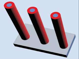
Yang and his group are able to reduce both the quantity and the quality requirements for silicon by using vertical arrays of nanostructured radial p-n junctions rather than conventional planar p-n junctions. In a radial p-n junction, a layer of n-type silicon forms a shell around a p-type silicon nanowire core. As a result, photo-excited electrons and holes travel much shorter distances to electrodes, eliminating a charge-carrier bottleneck that often arises in a typical silicon solar cell. The radial geometry array also, as photocurrent and optical transmission measurements by Yang and Garrett revealed, greatly improves light trapping.
"Since each individual nanowire in the array has a p-n junction, each acts as an individual solar cell," Yang says. "By adjusting the length of the nanowires in our arrays, we can increase their light-trapping path length."
While the conversion efficiency of these solar nanowires was only about five to six percent, Yang says this efficiency was achieved with little effort put into surface passivation, antireflection, and other efficiency-increasing modifications.
"With further improvements, most importantly in surface passivation, we think it is possible to push the efficiency to above 10 percent," Yang says.
Combining a 10 percent or better conversion efficiency with the greatly reduced quantities of starting silicon material and the ability to use metallurgical grade silicon, should make the use of silicon nanowires an attractive candidate for large-scale development.
As an added plus Yang says, "Our technique can be used in existing solar panel manufacturing processes." ###
This research was funded by the National Science Foundation's Center of Integrated Nanomechanical Systems.
Berkeley Lab is a U.S. Department of Energy national laboratory located in Berkeley, California. It conducts unclassified scientific research for DOE's Office of Science and is managed by the University of California. Visit our website at www.lbl.gov.
Contact: Lynn Yarris lcyarris@lbl.gov 510-486-5375 DOE/Lawrence Berkeley National Laboratory


No comments:
Post a Comment