Microchip manufacturers have long faced challenges miniaturizing transistors, the key active components in nearly every modern electronic device, which are used to amplify or switch electronic signals.
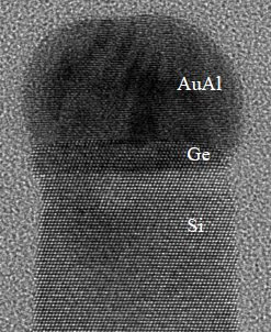
Now, researchers from the UCLA Henry Samueli School of Engineering and Applied Science, Purdue University and IBM have successfully grown silicon-germanium semiconducting nanowires for potential use in next-generation transistors.
These nanowires — which measure from a few tens to a few hundreds of nanometers in diameter and up to several millimeters in length — could help speed the development of smaller, faster and more powerful electronics, according to study co-author Suneel Kodambaka, a UCLA professor of materials science and engineering.
According to Kodambaka, silicon-germanium nanostructures also have thermoelectric applications, in which heat is converted into electricity.
"The Jet Propulsion Laboratory uses bulk chunks of silicon-germanium to power their satellites, and now there is a lot of interest in using a similar technology in automobiles. These nanowires have great potential in any area involving electronics," Kodambaka said.
To grow the silicon-germanium nanowires, tiny particles of a gold-aluminum alloy are first heated to temperatures above 370 degrees Celsius and melted inside a vacuum chamber. A silicon-containing gas is then introduced into the chamber, causing silicon to precipitate and form wires under the droplets. A germanium-containing gas is used to form the germanium wires.
"Think of it as ice growing from water vapor or the formation of ice crystals during a snow storm. You can get forests of ice wires under the right conditions instead of getting snow flakes or flat films of sleet," Kodambaka said. "But instead of water vapor, we introduced silicon vapor to get the silicon wire."
"The challenge was to create a really sharp interface between the silicon and germanium in each wire," Kodambaka said. "So we cooled the liquid droplets until they solidified. This allowed us to get rid of excess silicon in the alloy. Then, germanium wire segments could be grown on the silicon with the introduction of germanium vapor, and sharp interfaces formed."
The next step for the team is to grow the same structures over larger areas in a conventional growth reactor rather than in a tiny area under the microscope.
"This will allow my colleagues at IBM to process the wires into devices and measure their electronic properties," Ross said. "Of course, we would hope that the properties are improved, compared to conventional nanowires; and if this works out, we will look into new devices and try out different metal alloys to determine which is best for making devices." ###
The research was funded by the National Science Foundation through the NSF's Electronic and Photonic Materials Program in the Division of Materials Research, and also in part by the University of California Energy Institute (UCEI).
The UCLA Henry Samueli School of Engineering and Applied Science, established in 1945, offers 28 academic and professional degree programs, including an interdepartmental graduate degree program in biomedical engineering. Ranked among the top 10 engineering schools at public universities nationwide, the school is home to seven multimillion-dollar interdisciplinary research centers in wireless sensor systems, nanotechnology, nanomanufacturing and nanoelectronics, all funded by federal and private agencies.
Contact: Wileen Wong Kromhout wwkromhout@support.ucla.edu 310-206-0540 University of California - Los Angeles


No comments:
Post a Comment