Friday, October 30, 2009

Molecules on a string, and why size isn't the only thing that matters for data storage

Physicists get a grip on slippery molecules, and learn how the shape of nanoscopic magnetic islands affect data storage.

Molecules of hydrogen are difficult to steer with electric fields because of the symmetrical way that charges are distributed within them. But now researchers at ETH Zurich have found a clever technique to get a grip on the molecules. Their findings are reported in Physical Review Letters and highlighted in the September 14 issue of Physics (http://physics.aps.org).

Electric fields can easily manipulate electrically asymmetric molecules like water, but electric forces can't overcome thermal motions for highly symmetric molecules like H2.

Turbulent Convection

Caption: On the top is a shadowgraph visualization of rising and falling plumes in a turbulent fluid. On the bottom are small liquid-crystal spheres show the temperature and velocity in a fluid simultaneously.

Credit: Top image: X. D. Shang, X. L. Qiu, P. Tong, and K.-Q. Xia, Phys. Rev. Lett. 90, 074501 (2003); Bottom image Y. B. Du and P. Tong, J. Fluid Mech. 407, 57 (2000). Usage Restrictions: None.
In the 1980s, researchers in search of a way to manipulate non-polar molecules proposed a trick: excite one of H2's two electrons into a high orbit, disrupting the molecule's symmetry. The far-flung electron feels the pull of the electric field and drags the rest of the molecule along, rendering H2 as manageable as a puppet on a string.

Now Stephen Hogan, Christian Seiler, and Frederic Merkt at ETH Zurich have made this idea reality by overcoming a key problem: an electron in an excited orbit usually reverts to its ground state long before researchers can take advantage of the molecule's maneuverability. They studied several excited orbits in detail, found the longest-lasting ones, and used lasers to select these special states from a group of hydrogen molecules. The newly manageable molecules could be slowed down and trapped for 50 microseconds, plenty of time for the team to study them in detail.

Size isn't the only thing that matters for data storage

Minute magnetic particles, whether bonded to plastic tape or coated onto a hard disk, are the basis of modern data storage. Information is encoded in the magnetic orientation of these nanoparticles, but particles can sometimes switch orientations spontaneously, which can potentially corrupt data. Now researchers from Lawrence Berkeley and Argonne National Laboratories report that this switching unfolds in a more complicated manner than was previously thought. Their work is published in Physical Review Letters and highlighted in the September 14 issue of Physics (http://physics.aps.org).
Scientists have long known that spin flipping becomes more likely as the size of a nanoparticle cluster dwindles. But Stefan Krause and his team discovered that this is not the end of the story. Flipping happens as a kind of chain reaction along a cluster, and the shape of a cluster can help or hinder this propagation. Manipulating the shape of a cluster and even inserting impurities can determine whether a switch is more or less likely to be triggered and propagate, potentially adding a new dimension of control to the design of magnetic devices. ###

Also in Physics this week:

Guenter Ahlers writes a Trends article in Physics (physics.aps.org) on how the unexplored details of convection could hold the key to understanding nature's most impressive phenomena, such as sunspots and patterns in the sun's photosphere.

About APS Physics

APS Physics (physics.aps.org) publishes expert written commentaries and highlights of papers appearing in the journals of the American Physical Society

Contact: James Riordon riordon@aps.org 301-209-3238 American Physical Society

Wednesday, October 28, 2009

Looking deeply into polymer solar cells

Researchers from the Eindhoven University of Technology and the University of Ulm have made the first high-resolution 3D images of the inside of a polymer solar cell. This gives them important new insights in the nanoscale structure of polymer solar cells and its effect on the performance. The findings were published online in Nature Materials on Sunday 13 September.

The investigations shed new light on the operational principles of polymer solar cells.

Cost-effective, flexible and lightweight

Polymer Solar Cell

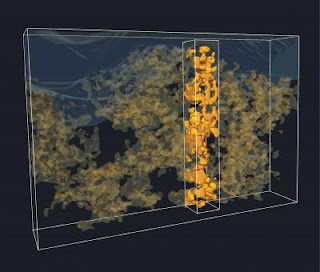
Caption: This is a 3-D electron tomography image of a polymer-metal oxide solar cell. The 3-D nanoscopic morphology shows the interpenetrating metal oxide network in (yellow) below an aluminum contact (gray) inside a polymer matrix (black).

Credit: Eindhoven University of Technology. Usage Restrictions: None.
These solar cells do not have the high efficiencies of their silicon counterparts yet. Polymer cells, however, can be printed in roll-to-roll processes, at very high speeds, which makes the technology potentially very cost-effective. Added to that, polymer cells are flexible and lightweight, and therefore suitable to be used on vehicles or clothing or to be incorporated in the design of objects.

Hybrid polymer solar cells

In these hybrid solar cells, a mixture of two different materials, a polymer and a metal oxide are used to create charges at their interface when the mixture is illuminated by the sun. The degree of mixing of the two materials is essential for its efficiency.
Intimate mixing enhances the area of the interface where charges are formed but at the same time obstructs charge transport because it leads to long and winding roads for the charges to travel. Larger domains do exactly the opposite. The vastly different chemical nature of polymers and metal oxides generally makes it very difficult to control the nanoscale structure. The Eindhoven researchers have been able to largely circumvent this problem by using a precursor compound that mixes with the polymer and is only converted into the metal oxide after it is incorporated in the photoactive layer. This allows better mixing and enables extracting up to 50% of the absorbed photons as charges in an external circuit.

Nanoscale mixing

The importance of the degree of mixing was clearly demonstrated by visualization of the structure of these blends in three dimensions. Traditionally such visualization has been extremely challenging, but by using 3D electron tomography, the team has been able to resolve the mixing with unprecedented detail on a nanoscale. From these images the researchers at the Institute of Stochastics in Ulm have been able to extract typical distances between the two components, relating to the efficiency of charge generation, and analyze the percolation pathways, that is, how much of each component is connected to the electrode. These quantitative analyses of the structure matched perfectly with the observed performance of the solar cells in sunlight.

Future

Even though these hybrid polymer solar cells are among the most efficient reported to date for this class, their power conversion efficiency of 2% in sunlight must be enhanced to make them really useful. This will be realized by improving the control over the morphology of the photoactive blend, for example by creating polymers that can interact with the metal oxide and by developing polymers or molecules that absorb a larger part of the solar spectrum. At such point, the intrinsic advantages of hybrid polymer solar cells in terms of low cost and thermal stability of the nanoscale structure could be fully exploited. ###

Publication

The publication "The effect of three-dimensional morphology on the efficiency of hybrid polymer solar cells", by Stefan Oosterhout et al. can be found at DOI 10.1038/NMAT2533.

The research was conducted at the Eindhoven University of Technology and the University of Ulm. It was funded by the Joint Solar Programme of FOM, NWO, and the Shell Research Foundation, the Deutsche Forschungsgemeinschaft, SenterNovem, and the Dutch Polymer Institute.

Contact: René Janssen r.a.j.janssen@tue.nl 31-622-455-438 Eindhoven University of Technology

Tuesday, October 27, 2009

When nano may not be nano

DURHAM, N.C. – The same properties of nanoparticles that make them so appealing to manufacturers may also have negative effects on the environment and human health.

However, little is known which particles may be harmful. Part of the problem is determining exactly what a nanoparticle is.

A new analysis by an international team of researchers from the Center for the Environmental Implications of NanoTechnology (CEINT), based at Duke University, argues for a new look at the way nanoparticles are selected when studying the potential impacts on human health and the environment. They have found that while many small particles are considered to be "nano," these materials often do not meet full definition of having special properties that make them different from conventional materials.

Mark Wiesner, Duke University

Caption: This is Mark Wiesner from Duke University.

Credit: Duke University Photography. Usage Restrictions: None.
Under the prevailing definition, a particle is deemed nano if its diameter is between 1 and 100 nanometers (nm) – about 1/10,000 the diameter of a human hair – and if it has properties that significantly differ from its naturally occurring, or bulk, counterpart.

The special properties of nanoparticles come from their high surface-area-to-volume ratio. They also have a considerably higher percentage of atoms on their surface compared to bulk particles, which can make them more reactive.
These man-made materials can be found in a vast array of consumer products, including paints and sunscreens, as well as in water treatment plants and drug delivery systems.

For most of this decade, discussions of nanoparticles have tended to focus more on their size than their properties. However, after reviewing the scientific literature, the Duke-led team believes that the old definition is not specific enough. A definition that focuses on properties is critical, they say, to help scientists determine which particular nanoparticles are the most likely to represent a threat to the environment or human health.

Generally speaking, it is the very smallest particles (less than 30 nanometers) that should receive the most attention in studying the environmental and human health impacts of nanomaterials, according to Mark Wiesner, a Duke professor of civil and environmental engineering and director of the federally funded CEINT.

"There are an infinite number of potential new man-made nanoparticles, so we need to find a way to narrow our efforts to those that have the greatest likelihood of having the unique properties with unique effects," Wiesner said.

"A key question to be answered is whether or not a particular nanoparticle has toxic or hazardous properties that are truly different from identical particles in their bulk form," Wiesner continued. "This question has not been answered. To do so, we need to be speaking the same language when assessing any unique properties of these novel materials."

The results of Wiesner's analysis were published online in the journal Nature Nanotechnology. The study was supported by CEINT, which is jointly funded by the National Science Foundation and Environmental Protection Agency.

Specifically, the researchers found that nanoparticles approaching the 100 nm end of the size spectrum tend to have fewer special properties when compared to their bulk counterparts. Furthermore, they found that nanoparticles smaller than 30 nm tend to exhibit the unique properties that should command increased scrutiny, Wiesner said.

"Many nanoparticles smaller than 30 nanometers undergo drastic changes in their crystalline structure that enhance how the atoms on their surface interact with the environment," Wiesner said.

For example, because of the increased surface-area-to-volume ratio, nanoparticles can be highly reactive with other chemicals in the environment and can also disrupt certain activities within cells.

"While there have been reports of nanoparticle toxicity increasing as the size decreases, it is still uncertain whether this increase in reactivity is harmful to the environment or human safety," Wiesner said. "To settle this issue, toxicological studies should contrast particles that exhibit novel size-dependant properties, particularly concerning their surface reactivity, and those particles that do not exhibit these properties." ###

Other members of the research team include Melanie Auffan, Duke; Jerome Rose and Jean-Yves Bottero, Aix-Marseille Universite, France; Gregory Lowry, Carnegie Mellon University; and Jean-Pierre Jolivet, Laboratoire de Chimie de la Matiere Condensee de Paris, France.

Contact: Richard Merritt richard.merritt@duke.edu 919-660-8414 Duke University

Monday, October 26, 2009

Gold solution for enhancing nanocrystal electrical conductance

Berkeley, CA - In a development that holds much promise for the future of solar cells made from nanocrystals, and the use of solar energy to produce clean and renewable liquid transportation fuels, researchers with the U.S. Department of Energy's Lawrence Berkeley National Laboratory (Berkeley Lab) have reported a technique by which the electrical conductivity of nanorod crystals of the semiconductor cadmium-selenide was increased 100,000 times.

"The key to our success is the fabrication of gold electrical contacts on the ends of cadmium-selenide rods via direct solution phase-growth of the gold tips," says Paul Alivisatos, interim-Director of Berkeley Lab, who led this research. "Solution-grown contacts provide an intimate, abrupt nanocrystal-metal contact free of surfactant, which means that unlike previous techniques for adding metal contacts, ours preserves the intrinsic semiconductor character of the starting nanocrystal."

Matt Sheldon,DOE/Lawrence Berkeley National Laboratory

Matt Sheldon,DOE Lawrence Berkeley National Laboratory

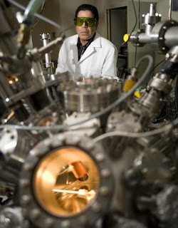
Caption: Matthew Sheldon, a member of the Paul Alivisatos research group, was part of Berkeley Lab research team that developed a technique by which the electrical conductivity of nanorod crystals of the semiconductor cadmium-selenide was increased 100,000 times.

Credit: Photo by Roy Kaltschmidt, Berkeley Lab Public Affairs. Usage Restrictions: None.
Alivisatos is a chemist who holds joint appointments with Berkeley Lab's Materials Sciences Division, and with the University of California-Berkeley where he is the Larry and Diane Bock professor of Nanotechnology. He is an internationally-recognized authority on nanocrystal growth and the corresponding author of a paper published in the on-line edition of Nano Letters entitled: "Enhanced Semiconductor Nanocrystal Conductance via Solution Grown Contacts."

Co-authoring the paper with Alivisatos were Matthew Sheldon and Paul-Emile Trudeau, members of Alivisatos' research group; Taleb Mokari, of Berkeley Lab's Molecular Foundry; and Lin-Wang Wang, in Berkeley Lab's Computational Research Division.

With the world demand for energy projected to more than double by 2050 and more than triple by the end of the 21st century, it is imperative that sustainable and carbon-neutral energy technologies be developed. The use of sunlight to generate electricity as well as to split water molecules for the production of fuels is envisioned as an ideal energy source, and nanocrystals could be pivotal to the success of this vision. Electrical conductance in semiconductor nanocrystals is a critical element for both solar electricity and solar fuel technologies.
"Standard contacting procedures that deposit metal onto semiconductor nanocrystals directly, such as those used in commercial wafer-scale chip fabrication, cause alloying and chemical reactions at the metal-semiconductor interface," says Sheldon, who was the lead author on the Nano Letters paper. "This means that the finished electrical device is actually made of a different material than the starting nanocrystal."

Sheldon notes that while chemical treatments, such as etching off surfactant, have been shown to enhance the conductivity of thin film nanocrystal solids, these treatments will often alter the semiconductor's electrical properties, for example switching the material from n-type to p-type or altering the density of surface states. Furthermore, he says, previous studies have not explained why electrical conductance was enhanced, other than acknowledging the removal of surfactant coverage.

In this new study, Sheldon, Alivisatos and their co-authors used single nanostructure electrical measurements to make systematic comparisons between cadmium-selenide nanorods with and without gold tips. The solution-grown tipping process started with the addition of gold salt to a solution of toluene and cadmium-selenide nanorods, which resulted in gold metal being selectively deposited on the nanorod tips. A silicon wafer test chip was then dipped in this nanorod solution. After submersion, the evaporation of the toulene solvent oriented individual cadmium-selenide nanorods across pre-defined gold electrodes, which were fabricated through electron beam lithography. The results were gold-tipped cadmium-selenide heterostructure devices whose electrical conductance was characterized in a two-terminal geometry as a function of source-drain voltage and temperature.

Says Alivisatos, "Our study shows that the superior performance of gold-tipped cadmium-selenide heterostructures results from a lower Schottky barrier and that solution grown contacts do not alter the chemical composition of the semiconductor. Further, our work demonstrates the increasing sophistication of high-quality electrical devices that can be achieved through self-assembly and verifies this process as an excellent route to the next generation of electronic and optoelectronic devices utilizing colloidal nanocrystals."

Adds Sheldon, "We believe our approach is an ideal strategy for making future devices from nanocrystals because it preserves the semiconductor character of the nanocrystal as synthesized with the precise control of their synthesis developed over the past decades."

Sheldon says the next step in this work will be to determine if the dramatic improvements in electrical behavior can translate to improvements in nanocrystal-based energy production. Initially, the group plans to investigate the use of solution grown contacts in photovoltaic applications. ###

This research was primarily funded by the DOE Office of Science through Berkeley Lab's Helios Solar Energy Research Center.

Berkeley Lab is a U.S. Department of Energy national laboratory located in Berkeley, California. It conducts unclassified scientific research for DOE's Office of Science and is managed by the University of California. Visit our Website at www.lbl.gov/

Contact: Lynn Yarris lcyarris@lbl.gov 510-486-5375 DOE/Lawrence Berkeley National Laboratory

Sunday, October 25, 2009

Electrical circuit runs entirely off power in trees

You've heard about flower power. What about tree power? It turns out that it's there, in small but measurable quantities. There's enough power in trees for University of Washington researchers to run an electronic circuit, according to results to be published in the Institute of Electrical and Electronics Engineers' Transactions on Nanotechnology.

"As far as we know this is the first peer-reviewed paper of someone powering something entirely by sticking electrodes into a tree," said co-author Babak Parviz, a UW associate professor of electrical engineering.

A study last year from the Massachusetts Institute of Technology found that plants generate a voltage of up to 200 millivolts when one electrode is placed in a plant and the other in the surrounding soil. Those researchers have since started a company developing forest sensors that exploit this new power source.

Babak Parviz, Brian Otis and Carlton Himes, University of Washington

Caption: Electrical engineers Babak Parviz and Brian Otis and undergraduate student Carlton Himes (right to left) demonstrate an electrical circuit that runs entirely off tree power.

Credit: University of Washington. Usage Restrictions: None.

Tree Power Circuit

Caption: This custom circuit is able to store up enough voltage from trees to be able to run a low-power sensor.

Credit: University of Washington. Usage Restrictions: None.
The UW team sought to further academic research in the field of tree power by building circuits to run off that energy. They successfully ran a circuit solely off tree power for the first time.

Co-author Carlton Himes, a UW undergraduate student, spent last summer exploring likely sites. Hooking nails to trees and connecting a voltmeter, he found that bigleaf maples, common on the UW campus, generate a steady voltage of up to a few hundred millivolts.

The UW team next built a device that could run on the available power. Co-author Brian Otis, a UW assistant professor of electrical engineering, led the development of a boost converter, a device that takes a low incoming voltage and stores it to produce a greater output. His team's custom boost converter works for input voltages of as little as 20 millivolts (a millivolt is one-thousandth of a volt), an input voltage lower than any existing such device. It produces an output voltage of 1.1 volts, enough to run low-power sensors.

The UW circuit is built from parts measuring 130 nanometers and it consumes on average just 10 nanowatts of power during operation (a nanowatt is one billionth of a watt).
"Normal electronics are not going to run on the types of voltages and currents that we get out of a tree. But the nanoscale is not just in size, but also in the energy and power consumption," Parviz said.

"As new generations of technology come online," he added, "I think it's warranted to look back at what's doable or what's not doable in terms of a power source."

Despite using special low-power devices, the boost converter and other electronics would spend most of their time in sleep mode in order to conserve energy, creating a complication.

"If everything goes to sleep, the system will never wake up," Otis said.

To solve this problem Otis' team built a clock that runs continuously on 1 nanowatt, about a thousandth the power required to run a wristwatch, and when turned on operates at 350 millivolts, about a quarter the voltage in an AA battery. The low-power clock produces an electrical pulse once every few seconds, allowing a periodic wakeup of the system.

The tree-power phenomenon is different from the popular potato or lemon experiment, in which two different metals react with the food to create an electric potential difference that causes a current to flow.

"We specifically didn't want to confuse this effect with the potato effect, so we used the same metal for both electrodes," Parviz said.

Tree power is unlikely to replace solar power for most applications, Parviz admits. But the system could provide a low-cost option for powering tree sensors that might be used to detect environmental conditions or forest fires. The electronic output could also be used to gauge a tree's health.

"It's not exactly established where these voltages come from. But there seems to be some signaling in trees, similar to what happens in the human body but with slower speed," Parviz said. "I'm interested in applying our results as a way of investigating what the tree is doing. When you go to the doctor, the first thing that they measure is your pulse. We don't really have something similar for trees." ###

Other co-authors are Eric Carlson and Ryan Ricchiuti of the UW. The research was funded in part by the National Science Foundation.

For more information, contact Parviz at 206-616-4038 or babak@ee.washington.edu or Otis at 206-616-5998 or botis@ee.washington.edu

Friday, October 23, 2009

Analysis confirms that nano-related research has strong multidisciplinary roots

Mapping nanotechnology, The burgeoning research fields of nanoscience and nanotechnology are commonly thought to be highly multidisciplinary because they draw on many areas of science and technology to make important advances.

Research reported in the September issue of the journal Nature Nanotechnology finds that nanoscience and nanotechnology indeed are highly multidisciplinary – but not much more so than other modern disciplines such as medicine or electrical engineering that also draw on multiple areas of science and technology.

With $1.6 billion scheduled to be invested in nano-related research during 2010, assessing the multidisciplinary nature of the field could be important to policy-makers, research managers, technology-transfer officers and others responsible for managing the investment and creating a supportive environment for it.

Nanopapers

Caption: This figure shows the position of nanoscience and nanotechnology over a base map of science. Each node is one of 175 subject categories in the SCI database, and the size of the node is proportional to the number of nanopapers published.

Credit: Courtesy Alan Porter and Jan Youtie. Usage Restrictions: None.

Fields of Science

Caption: This figure shows the fields of science cited by nanotechnology papers.

Credit: Courtesy Alan Porter and Jan Youtie. Usage Restrictions: None.
"Research in nanoscience and nanotechnology is not just a collection of isolated 'stove pipes' drawing knowledge from one narrow discipline, but rather is quite interdisciplinary," said Alan Porter, co-author of the paper and a professor emeritus in the Schools of Industrial and Systems Engineering and Public Policy at the Georgia Institute of Technology. "We found that research in any one category of nanoscience and nanotechnology tends to cite research in many other categories."

The study was sponsored by the National Science Foundation through the Center for Nanotechnology in Society at Arizona State University.

Porter and collaborator Jan Youtie, manager of policy services in Georgia Tech's Enterprise Innovation Institute, analyzed abstracts from more than 30,000 papers with "nano" themes that were published between January and July of 2008. They found that although materials science and chemistry dominated the papers, fields as diverse as clinical medicine, biomedical sciences and physics also contributed.
These "nanopapers" studied by the researchers appeared in more than 6,000 journals that were part of a database known as the Science Citation Index (SCI). The researchers found nanopapers in 151 of SCI's 175 subject categories, with 52 of the categories containing more than 100 such papers.

To explore how well knowledge was integrated across the disciplines, the researchers also studied the journal articles that were cited in the nanopapers. They found more than one million cited references, a mean of 33 per paper.

Using text mining techniques to extract sources from the cited references, they further found that 45 subject categories were cited by five percent or more of the nanopapers – and 98 categories that were cited by at least one percent of the papers. The text mining was done using VantagePoint software developed by Georgia Tech and Search Technology Inc.

Six subject categories dominated both the original nanopapers and the cited references. Each of the six contained 10 percent or more of the original nanopapers and was cited by 39 percent or more of the references. They are:

* Materials science, multidisciplinary
* Physics, applied
* Chemistry, physical
* Physics, condensed matter
* Nanoscience and nanotechnology
* Chemistry, multidisciplinary

The researchers found considerable interdisciplinary representation within those six categories. Though 86 percent of the 3,863 nanopapers in the "nanoscience and nanotechnology" category cited papers in materials science, another 80 subject categories had 40 or more cited papers each.

This representation continued even outside the top six categories. The 808 nanopapers in electrical engineering cited papers in journals from 138 different subject categories, while the 435 nanopapers in organic chemistry cited papers in journals from 140 different subject categories.

The researchers also used a metric they called an "integration score" to gauge how interdisciplinary nature of a particular paper or set of papers. The integration score ranged from zero for stand-alone disciplines that don't cite work from other disciplines to one for highly-integrated disciplines that heavily cite work from other areas.

Integration scores ranged from 0.65 for nanoscience and nanotechnology to 0.60 for electrical engineering and 0.64 for organic chemistry.

"Our results show the multidisciplinary nature of research in nanoscience and nanotechnology, although the integration scores make it clear that much non-nano research is also comparably interdisciplinary," Porter said. "Much of the nanoresearch is also concentrated in 'macrodisciplines' such as materials science and chemistry, and researchers tend to cite work from neighboring fields more often than work in more distant fields."

Understanding the interdisciplinary nature of nanoscience and nanotechnology could be important to creating the right environment for the field to produce results.

"There is a broad perspective that most scientific breakthroughs occur at the interstices among more established fields," said Youtie. "Nanotechnology R&D is believed to be an area where disciplines converge. If nanotechnology does have a strong multidisciplinary character, attention to communication across disciplines will be an important feature in its emergence."

In the future, Porter and Youtie hope to explore other policy-focused nano topics, including:

* How research and development patterns can forecast likely commercial innovations;
* The societal implications of nanoscience and nanotechnology innovations so that potential negative efforts can be mitigated before they occur;
* How corporations develop their strategies for nanoscience and nanotechnology, and
* Where nanoscience and hotspots for research and development – called "nanodistricts" – exist around the world.

"A nanodistrict is a regional concentration of research institutions and firms where nanotechnologies are developed," Youtie explained. "Although nanotechnology applications are deployed widely across the world, a smaller number of nanodistrict locations are appearing where nanotechnology research, development and initial commercialization are clustered." ###

The Center for Nanotechnology in Society is part of a broad U.S. effort to anticipate the societal implications of nanotechnology. Georgia Tech's role in the multi-university effort is to characterize the type of nanotechnology research being done and to identify early indicators of emerging technologies in that field.

Youtie and Porter are also part of Georgia Tech's Program in Science, Technology and Innovation Policy (STIP), a collaboration of the School of Public Policy and the Enterprise Innovation Institute that advances research and practice in science, technology, innovation and spatial development policy.

The findings and opinions contained in this news release are those of the researchers and do not necessarily reflect the views of the National Science Foundation (NSF).

Contact: John Toon jtoon@gatech.edu 404-894-6986 Georgia Institute of Technology Research News

Wednesday, October 21, 2009

Promise of Nanodiamonds for Safer Gene Therapy

Researchers are looking for better ways to deliver treatments for a variety of diseases. Nanodiamonds may be the key to a viable solution.

EVANSTON, Ill. --- Gene therapy holds promise in the treatment of a myriad of diseases, including cancer, heart disease and diabetes, among many others. However, developing a scalable system for delivering genes to cells both efficiently and safely has been challenging.

Now a team of Northwestern University researchers has introduced the power of nanodiamonds as a novel gene delivery technology that combines key properties in one approach: enhanced delivery efficiency along with outstanding biocompatibility.

Professor Dean Ho

Dean Ho, Ph.D. Assistant Professor Departments of Biomedical and Mechanical Engineering Robert R. McCormick School of Engineering and Applied Science
Northwestern University.
"Finding a more efficient and biocompatible method for gene delivery than is currently available is a major challenge in medicine," said Dean Ho, who led the research. "By harnessing the innate advantages of nanodiamonds we now have demonstrated their promise for gene therapy."

Ho is an assistant professor of biomedical engineering and mechanical engineering in the McCormick School of Engineering and Applied Science and a member of the Robert H. Lurie Comprehensive Cancer Center of Northwestern University.

Ho and his research team engineered surface-modified nanodiamond particles that successfully and efficiently delivered DNA into mammalian cells. The delivery efficiency was 70 times greater than that of a conventional standard for gene delivery. The new hybrid material could impact many facets of nanomedicine.
The results are published online by the journal ACS Nano.

"A low molecular weight polymer called polyethyleneimine-800 (PEI800) currently is a commercial approach for DNA delivery," said Xue-Qing Zhang, a postdoctoral researcher in Ho's group and the paper's first author. "It has good biocompatibility but unfortunately is not very efficient at delivery. Forms of high molecular weight PEI have desirable high DNA delivery efficiencies, but they are very toxic to cells."

Multiple barriers confront conventional approaches, making it difficult to integrate both high-efficiency delivery and biocompatibility into one gene delivery system. But the Northwestern researchers were able to do just that by functionalizing the nanodiamond surface with PEI800.

The combination of PEI800 and nanodiamonds produced a 70 times enhancement in delivery efficiency over PEI800 alone, and the biocompatibility of PEI800 was preserved. The process is highly scalable, which holds promise for translational capability.

The researchers used a human cervical cancer cell line called HeLa to test the efficiency of gene delivery using the functionalized nanodiamonds. Glowing green cells confirmed the delivery and insertion into the cells of a "Green Fluorecent Protein (GFP)"-encoding DNA sequence. This served as a demonstrative model of how specific disease-fighting DNA strands could be delivered to cells. As a platform, the nanodiamond system can carry a broad array of DNA strands.

Regarding toxicity measurements, cellular viability assays showed that low doses of the toxic high-molecular PEI resulted in significant cell death, while doses of nanodiamond-PEI800 that were three times higher than that of the high-molecular weight PEI revealed a highly biocompatible complex.

Ho and his research team originally demonstrated the application of nanodiamonds for chemotherapeutic delivery and subsequently discovered that the nanodiamonds also are extremely effective at delivering therapeutic proteins. Their work further has shown that nanodiamonds can sustain delivery while enhancing their specificity as well.

Having demonstrated the safety of nanodiamonds and their applicability toward a variety of biological uses, Ho's team is pursuing aggressively the steps necessary to push them towards clinical relevance. Current studies are boosting the targeting capabilities of the nanodiamonds while also evaluating their pre-clinical efficiency.

"There's a long road ahead before the technology is ready for clinical use," Ho said, "but we are very pleased with the exciting properties and potential of the nanodiamond platform." ###

The National Science Foundation, the Wallace H. Coulter Foundation and the V Foundation for Cancer Research supported the research.

The title of the ACS Nano paper is "Polymer-Functionalized Nanodiamond Platforms as Vehicles for Gene Delivery." In addition to Ho (senior author) and Zhang, other authors of the paper are Mark Chen, Robert Lam and Xiaoyang Xu, all from Northwestern, and Eiji Osawa, from the NanoCarbon Research Institute at Shinshu University, Nagano, Japan.

Contact: Megan Fellman fellman@northwestern.edu 847-491-3115 Northwestern University

Monday, October 19, 2009

Hankering for molecular electronics? Grab the new NIST sandwich

The sandwich recipe recently concocted by scientists working at the National Institute of Standards and Technology (NIST) may prove tasty for computer chip designers, who have long had an appetite for molecule-sized electronic components – but no clear way to satisfy it until now.

The research team, which includes collaborators from the University of Maryland, has found a simple method of sandwiching organic molecules between silicon and metal, two materials fundamental to electronic components. By doing so, the team may have overcome one of the principal obstacles in creating switches made from individual molecules, which represent perhaps the ultimate in miniaturization for the electronics industry.

Molecular Electronics

Caption: The flip-chip lamination method creates an ultra-smooth gold surface, which allows the organic molecules to form a thin yet even layer between the gold and silicon.

Credit: Coll Bau, NIST. Usage Restrictions: None.

Molecular Electronics

Caption: Gold surfaces created by other methods are substantially rougher, and would result in many of the molecular switches either being smashed or not contacting the silicon.

Credit: Coll Bau, NIST. Usage Restrictions: None.
The idea of using molecules as switches has been around for years, carrying the promise of components that can be produced cheaply in huge numbers, perform faster as a group than their larger silicon brethren, and use only a tiny fraction of their energy. But although there has been progress in creating the switching molecules themselves, the overall concept has been stuck on drawing boards in large part because organic molecules are delicate and tend to be damaged irreparably when subjected to one particularly stressful step in the chip-building process: attaching them to electrical contacts.

Metal forms many of these contacts in chip circuits, but getting metal onto a chip involves heating it until it evaporates, then allowing it to condense on the silicon. “Imagine what hot steam would do to your arm,” says Mariona Coll Bau, a materials scientist at NIST. “Evaporated metal is much hotter, and organic switching molecules are very fragile—they can’t stand the heat.”

Coll Bau’s team, however, found a way to cool the kitchen. They cover a surface with a non-stick material before condensing gold on top of it, allowing the metal to cool to an ultra-smooth surface. They then laminate the gold surface with the plastic used in overhead transparencies. The non-stick layer allows them to remove the laminated gold from the surface as easily as peeling off plastic wrap. Adding the organic molecules then is comparatively simple: attach the molecules to the gold and then flip the whole assembly onto a silicon base, with the organic molecules sandwiched neatly inside—and intact.
Though scientists have attempted to make sandwiches of this sort before, Coll Bau says their first-ever use of an imprinting machine finally made it possible to assemble the ingredients effectively. “The machine allows us to press the three layers together so the organic molecules contact both the silicon and gold, but without smashing or otherwise degrading them,” she says.

Coll Bau adds that “flip-chip lamination,” as the team calls it, could lead to applications beyond chip design, including biosensors, which depend on the organic and electronic worlds interacting. “The technique may prove useful as a fabrication paradigm,” she says. “It’s hard to make small things, and this might be an easier way to make them.” ###

* M. Coll, L.H. Miller, L.J. Richter, D.R. Hines, O.D. Jurchescu, N. Gergel-Hackett, C. Richter and C.A. Hacker. Formation of silicon-based molecular electronic structures using flip-chip lamination. Journal of the American Chemical Society, Aug. 11, 2009 (online publication), DOI 10.1021/ja901646j.

Contact: Chad Boutin boutin@nist.gov 301-975-4261 National Institute of Standards and Technology (NIST)

Sunday, October 18, 2009

Dartmouth researchers propose new way to reproduce a black hole PODCAST

HANOVER, NH – Despite their popularity in the science fiction genre, there is much to be learned about black holes, the mysterious regions in space once thought to be absent of light. In a paper published in the August 20 issue of Physical Review Letters, the flagship journal of the American Physical Society, Dartmouth researchers propose a new way of creating a reproduction black hole in the laboratory on a much-tinier scale than their celestial counterparts.

The new method to create a tiny quantum sized black hole would allow researchers to better understand what physicist Stephen Hawking proposed more than 35 years ago: black holes are not totally void of activity; they emit photons, which is now known as Hawking radiation.

Miles Blencowe (photo by Joseph Mehling '69)

Miles Blencowe (photo by Joseph Mehling '69) Podcast: Reproducing a Black Hole in the Laboratory, and other Quantum Theories (19:15, 17.6mb)
"Hawking famously showed that black holes radiate energy according to a thermal spectrum," said Paul Nation, an author on the paper and a graduate student at Dartmouth. "His calculations relied on assumptions about the physics of ultra-high energies and quantum gravity. Because we can't yet take measurements from real black holes, we need a way to recreate this phenomenon in the lab in order to study it, to validate it."

In this paper, the researchers show that a magnetic field-pulsed microwave transmission line containing an array of superconducting quantum interference devices, or SQUIDs, not only reproduces physics analogous to that of a radiating black hole, but does so in a system where the high energy and quantum mechanical properties are well understood and can be directly controlled in the laboratory.
The paper states, "Thus, in principle, this setup enables the exploration of analogue quantum gravitational effects."

"We can also manipulate the strength of the applied magnetic field so that the SQUID array can be used to probe black hole radiation beyond what was considered by Hawking," said Miles Blencowe, another author on the paper and a professor of physics and astronomy at Dartmouth.

This is not the first proposed imitation black hole, says Nation. Other proposed analogue schemes have considered using supersonic fluid flows, ultracold bose-einstein condensates and nonlinear fiber optic cables. However, the predicted Hawking radiation in these schemes is incredibly weak or otherwise masked by commonplace radiation due to unavoidable heating of the device, making the Hawking radiation very difficult to detect. "In addition to being able to study analogue quantum gravity effects, the new, SQUID-based proposal may be a more straightforward method to detect the Hawking radiation," says Blencowe. ###

In addition to Nation and Blencowe, other authors on the paper include Alexander Rimberg at Dartmouth and Eyal Buks at Technion in Haifa, Israel.

Contact: Sue Knapp sue.knapp@dartmouth.edu 603-646-3661 Dartmouth College

Friday, October 16, 2009

Let there be light: Teaching magnets to do more than just stick around

That palm tree magnet commemorating your last vacation is programmed for a simple function – to stick to your refrigerator. Similarly, semiconductors are programmed to convey bits of information small and large, processing information on your computer or cell phone.

Scientists are working to coax those semiconductors to be more than conveyers, to actually perform some functions like magnets, such as data recording and electronic control. So far most of those effects could only be achieved at very cold temperatures: minus 260 degrees Celsius or more than 400 below zero Fahrenheit, likely too cold for most computer users.

Daniel R. Gamelin

Daniel R. Gamelin
However, researchers led by a University of Washington chemist report Friday (Aug. 21) in Science that they have been able to train tiny semiconductor crystals, called nanocrystals or quantum dots, to display new magnetic functions at room temperature using light as a trigger.

Silicon-based semiconductor chips incorporate tiny transistors that manipulate electrons based on their charges.
Scientists also are working on ways to use electricity to manipulate the electrons' magnetism, referred to as "spin," but are still searching for the breakthrough that will allow "spintronics" to function at room temperature without losing large amounts of the capability they have at frigid temperatures.

The team led by Daniel Gamelin, a UW chemistry professor, has found a way to use photons – tiny light particles – to manipulate the magnetism of semiconductor nanocrystals efficiently, even up to room temperature.

"This provides a completely new approach to microelectronics, if you can use spin instead of charge to process information and use photons to manipulate that process," Gamelin said. "It opens the door to materials that store information and perform logic functions at the same time without the need for super cooling."

The team used nanocrystals of a cadmium-selenium semiconductor called cadmium selenide, but replaced some nonmagnetic cadmium ions with magnetic manganese ions. The crystals, smaller than 10 nanometers across (a nanometer is one-billionth of an inch), were then suspended in a colloid solution, like droplets of cream suspended in milk.

Beams of photons were used to align all of the manganese ions' spins, creating magnetic fields as much as 500 times more powerful than in the same semiconductor material without manganese. The magnetic effects were strongest at low temperatures, but remained remarkably strong up to room temperature, Gamelin said.

Besides Gamelin, authors of the Science paper are RĂ©mi Beaulac and Paul Archer of the UW and Lars Schneider and Gerd Bacher of the University of Duisburg-Essen in Germany.

In a second paper published Sunday (Aug. 16) in the online edition of Nature Nanotechnology, Gamelin's group reported related effects in semiconductor nanocrystals made of zinc oxide but also containing small amounts of manganese impurities.

With zinc oxide, photons acted more as an on-off switch – once photons altered the zinc oxide's magnetism, the photon stream could be removed and the effect remained in place until another stimulus was applied to turn the effect off again.

Besides Gamelin, authors of the Nature Nanotechnology paper are Stefan Ochsenbein, Yong Feng, Kelly Whitaker, Ekaterina Badaeva, William Liu and Xiaosong Li, all of the UW.

Some behaviors described in the papers have been seen previously at very low temperatures, but in those cases the active materials were embedded in other crystals and so could not be isolated or processed. Suspending the nanocrystals in a colloid solution brings the magnetic effects into a new functional form that could be useful for integration with unconventional materials, Gamelin said. For example, the solution containing the crystals could be applied to a film using a device like an ink jet printer, or interfaced with carbon-based materials using techniques not typically practical for magnetic semiconductors.

"We've brought these spin effects into a processable form," he said. "I think both of these papers are converging on the same applications. We're exploring how to manipulate spins in these nanostructures and perhaps opening the door for some exciting new technologies." ###

Funding for the work in the two papers came from the U.S. National Science Foundation, the Dreyfus Foundation, the Sloan Foundation, the Natural Sciences and Engineering Research Council of Canada, the German Research Foundation, Gaussian Inc., the Research Corp., the Swiss National Science Foundation and the University of Washington.

For more information, contact Gamelin at 206-685-0901 or gamelin@chem.washington.edu

Contact: Vince Stricherz vinces@u.washington.edu 206-543-2580 University of Washington

Wednesday, October 14, 2009

Nuclear fusion research key to advancing computer chips

WEST LAFAYETTE, Ind. - Researchers are adapting the same methods used in fusion-energy research to create extremely thin plasma beams for a new class of "nanolithography" required to make future computer chips.

Current technology uses ultraviolet light to create the fine features in computer chips in a process called photolithography, which involves projecting the image of a mask onto a light-sensitive material, then chemically etching the resulting pattern.

New nanolithography will be needed to continue advances in computer technology and to extend Moore's law, an unofficial rule stating that the number of transistors on integrated circuits, or chips, doubles about every 18 months.

Ahmed Hassanein, Purdue University

Caption: Nuclear engineer Ahmed Hassanein works at his Purdue lab, where researchers are adapting the same methods used in fusion-energy research to develop a new type of "nanolithography" for creating future computer chips. Supercomputers at the US Department of Energy's Argonne National Laboratory are needed to run simulations critical for the research. The technology revolves around extremely thin plasma beams for making tiny features in future computer chips and continuing Moore's law, an unofficial rule stating that the number of transistors on integrated circuits, or chips, doubles about every 18 months.

Credit: Purdue University photo/Vincent Walter. Usage Restrictions: None.
"We can't make devices much smaller using conventional lithography, so we have to find ways of creating beams having more narrow wavelengths," said Ahmed Hassanein, the Paul L. Wattelet Professor of Nuclear Engineering and head of Purdue's School of Nuclear Engineering.

The new plasma-based lithography under development generates "extreme ultraviolet" light having a wavelength of 13.5 nanometers, less than one-tenth the size of current lithography, Hassanein said.

Nuclear engineers and scientists at Purdue and the U.S. Department of Energy's Argonne National Laboratory are working to improve the efficiency of two techniques for producing the plasma: One approach uses a laser and the other "discharge-produced" method uses an electric current.

"In either case, only about 1 to 2 percent of the energy spent is converted into plasma," Hassanein said. "That conversion efficiency means you'd need greater than 100 kilowatts of power for this lithography, which poses all sorts of engineering problems. We are involved in optimizing conversion efficiency - reducing the energy requirements - and solving various design problems for the next-generation lithography."

Findings are detailed in a research paper scheduled to appear in the October-December 2009 issue of the Journal of Micro/Nanolithography, MEMS, and MOEMS. The paper was written by Hassanein, senior research scientist Valeryi Sizyuk, computer analyst Tatyana Sizyuk, and research assistant professor Sivanandan Harilal, all in the School of Nuclear Engineering.
Critical to the research is a computer simulation, called HEIGHTS - for high-energy interaction with general heterogeneous target systems - developed by Hassanein's team. Computations for a single HEIGHTS simulation using Argonne supercomputers can take several months to finish, said Hassanein, a former Argonne senior scientist who led work there to develop HEIGHTS.

The laser method creates plasma by heating xenon, tin or lithium. The plasma produces high-energy packets of light, called photons, of extreme ultraviolet light.

Plasma is a partially ionized gaslike material that conducts electricity. Because of this electrical conductivity, researchers are able to use magnetic fields to shape and control plasmas, forming beams, filaments and other structures. In experimental fusion reactors, magnetic fields are used to keep plasma-based nuclear fuel from touching the metal walls of the containment vessel, enabling the plasma to be heated to the extreme temperatures required to maintain fusion reactions.

HEIGHTS simulates the entire process of the plasma evolution: the laser interacting with the target, and the target evaporating, ionizing and turning into a plasma. The simulation also shows what happens when the magnetic forces "pinch" the plasma cloud into a smaller diameter spot needed to generate the photons.

Findings in the paper detail the laser-produced plasma beams, showing that simulations match data from laboratory experiments recently built at Purdue, Hassanein said.

"It was very exciting to see this match because it means we are on the right track," Hassanein said. "The computer simulations tell us how to optimize the entire system and where to go next with the experiments to verify that."

One design challenge stems from the fact that lenses absorb the photons that make up light, meaning they cannot be used to focus the beam. Instead, mirrors are used in the design. However, plasma condenses on the mirrors, reducing their reflectivity and limiting the efficiency of the process.

"We are trying to help find innovative ways of producing these photons, optimizing the production and mitigating the effects of the plasma on the mirrors," Hassanein said. "So we are trying to improve the entire system."

The simulation tool combines computations in plasma physics, radiation transport, atomic physics, plasma-material interactions and magnetohydrodynamics, or what happens when a target is heated, melts and turns into a plasma. ###

The work is based at the Center for Materials Under Extreme Environments at Purdue. Previous support came from Intel Corp and Sematech, an industry consortium formed to advance computer technology.

Writer: Emil Venere, 765-494-4709, venere@purdue.edu, Source: Ahmed Hassanein, 765 494-5742, hassanein@purdue.edu

Related Web sites: Contact: Emil Venere venere@purdue.edu 765-494-4709 Purdue University

Monday, October 12, 2009

New material for nanoscale computer chips

Nanochemists from the Chinese Academy of Sciences and Nano-Science Center, Department of Chemistry at University of Copenhagen have developed nanoscale electric contacts out of organic and inorganic nanowires. In the contact they have crossed the wires like Mikado sticks and coupled several contacts together in an electric circuit. In this way they have produced prototype computer electronics on the nanoscale.

Alternative to silicon computers

Today the foundation of our computers, mobile phones and other electronic apparatus is silicon transistors. A transistor is in principal an on- and off- contact and there are millions of tiny transistors on every computer chip. However, we are reaching the limit for how small we can make transistors out of silicon.

Prototype Computer Chip

Caption: Researchers cross organic and non-organic nanowires like Mikado sticks and thereby make nanoscale prototype computer electronics. Credit: Asmus Dohn. Usage Restrictions: Due credit.
We already use various organic materials in, for example, flat screens, such as OLED (Organic Light Emitting Diode). The new results show how small and advanced devices made of organic materials can become.

Thomas Bjørnholm, Director of the Nano-Science Center, Department of Chemistry at University of Copenhagen explains:

We have succeeded in placing several transistors consisting of nanowires together on a nano device. It is a first step towards realisation of future electronic circuitry based on organic materials – a possible substitute for today's silicon-based technologies. This offers the possibility of making computers in different ways in the future.

Danish-Chinese nanoelectronics

The researchers have used organic nanowires combined with the tin oxide nanowires in a so-called hybrid circuit.
As in a Mikado game, the nanowires cross in a device consisting of 4-6 active transistor moieties. The devices have a low operational current, high mobility and good stability and that is essential in order for the material to be able to compete with silicon.

Professor Wenping Hu, Chinese Academy of Sciences is excited over the results:

This work is the first significant result of our collaboration with the researchers from the Nano-Science Center. It is a good starting point for our new Danish-Chinese research centre for molecular nano-electronics and it underlines the fact that we can complement each other and that together we can achieve exciting and important results. ###

Contact: Thomas Bjørnholm tb@nano.ku.dk 453-532-1835 University of Copenhagen

Saturday, October 10, 2009

Nanomagnets guide stem cells to damaged tissue

Microscopic magnetic particles have been used to bring stem cells to sites of cardiovascular injury in a new method designed to increase the capacity of cells to repair damaged tissue, UCL scientists announced today.

The cross disciplinary research, published in The Journal of the American College of Cardiology: Cardiovascular Interventions, demonstrates a technique where endothelial progenitor cells – a type of stem cell shown to be important in vascular healing processes – have been magnetically tagged with a tiny iron-containing clinical agent, then successfully targeted to a site of arterial injury using a magnet positioned outside the body.

image of a human cell

Image: Microscopic image of a human cell (green cytoplasm, blue nucleus) loaded with mini-magnets (red).
Following magnetic targeting, there was a five-fold increase in cell localisation at a site of vascular injury in rats. The team also demonstrated a six-fold increase in cell capture in an in vitro flow system (where microscopic particles are suspended in a stream of fluid and examined to see how they behave).

Although magnetic fields have been used to guide cellular therapies, this is the first time cells have been targeted using a method directly applicable to clinical practice.
The technique uses an FDA (U.S. Food and Drug Administration) approved agent that is already used to monitor cells in humans using MRI (magnetic resonance imaging).

Dr Mark Lythgoe, UCL Centre for Advanced Biomedical Imaging, the senior author on the study, said: "Because the material we used in this method is already FDA approved we could see this technology being applied in human clinical trials within 3-5 years. It's feasible that heart attacks and other vascular injuries could eventually be treated using regular injections of magnetised stem cells. The technology could be adapted to localise cells in other organs and provide a useful tool for the systemic injection of all manner of cell therapies. And it's not just limited to cells – by focusing tagged antibodies or viruses using this method, cancerous tumours could be much more specifically targeted"

Panagiotis Kyrtatos, also from the UCL Centre for Advanced Biomedical Imaging and lead researcher of the study, added: "This research tackles one of the most critical challenges in the biomedical sciences today: ensuring the effective delivery and retention of cellular therapies to specific targets within the body.

"Cell therapies could greatly benefit from nano-magnetic techniques which concentrate cells where they are needed most. The nano-magnets not only assist with the targeting, but with the aid of MRI also allow us to observe how the cells behave once they're injected."

This work was supported by public and charitable funding from the UCL Institute of Child Health (Child Health Research Appeal Trust), The British Heart Foundation, the Alexander S. Onassis Public Benefit Foundation and the Biotechnology and Biological Sciences Research Council (BBSRC). ###

About UCL (University College London)

Founded in 1826, UCL was the first English university established after Oxford and Cambridge, the first to admit students regardless of race, class, religion or gender, and the first to provide systematic teaching of law, architecture and medicine. UCL is the seventh-ranked university in the 2008 THES-QS World University Rankings, and the third-ranked UK university in the 2008 league table of the top 500 world universities produced by the Shanghai Jiao Tong University. UCL alumni include Marie Stopes, Jonathan Dimbleby, Lord Woolf, Alexander Graham Bell, and members of the band Coldplay. UCL currently has over 12,000 undergraduate and 8,000 postgraduate students. Its annual income is over £600 million. www.ucl.ac.uk

Contact: Ruth Howells ruth.howells@ucl.ac.uk 44-020-767-99739 University College London

Thursday, October 08, 2009

New nanolaser key to future optical computers and technologies

Because the new device, called a "spaser," is the first of its kind to emit visible light, it represents a critical component for possible future technologies based on "nanophotonic" circuitry, said Vladimir Shalaev, the Robert and Anne Burnett Professor of Electrical and Computer Engineering at Purdue University.

Such circuits will require a laser-light source, but current lasers can't be made small enough to integrate them into electronic chips. Now researchers have overcome this obstacle, harnessing clouds of electrons called "surface plasmons," instead of the photons that make up light, to create the tiny spasers.

Findings are detailed in a paper appearing online Sunday (Aug. 16) in the journal Nature, reporting on work conducted by researchers at Purdue, Norfolk State University and Cornell University.

nanophotonic circuitry.

IMAGE CAPTION: Researchers have created the tiniest laser since its invention nearly 50 years ago. Because the new device, called a "spaser," is the first of its kind to emit visible light, it represents a critical component for possible future technologies based on "nanophotonic" circuitry. The color diagram (a) shows the nanolaser's design: a gold core surrounded by a glasslike shell filled with green dye.

Scanning electron microscope images (b and c) show that the gold core and the thickness of the silica shell were about 14 nanometers and 15 nanometers, respectively. A simulation of the SPASER (d) shows the device emitting visible light with a wavelength of 525 nanometers. (Birck Nanotechnology Center, Purdue University)
Nanophotonics may usher in a host of radical advances, including powerful "hyperlenses" resulting in sensors and microscopes 10 times more powerful than today's and able to see objects as small as DNA; computers and consumer electronics that use light instead of electronic signals to process information; and more efficient solar collectors.

"Here, we have demonstrated the feasibility of the most critical component - the nanolaser - essential for nanophotonics to become a practical technology," Shalaev said.

The "spaser-based nanolasers" created in the research were spheres 44 nanometers, or billionths of a meter, in diameter - more than 1 million could fit inside a red blood cell. The spheres were fabricated at Cornell, with Norfolk State and Purdue performing the optical characterization needed to determine whether the devices behave as lasers.
The findings confirm work by physicists David Bergman at Tel Aviv University and Mark Stockman at Georgia State University, who first proposed the spaser concept in 2003.

"This work represents an important milestone that may prove to be the start of a revolution in nanophotonics, with applications in imaging and sensing at a scale that is much smaller than the wavelength of visible light," said Timothy D. Sands, the Mary Jo and Robert L. Kirk Director of the Birck Nanotechnology Center in Purdue's Discovery Park.

The spasers contain a gold core surrounded by a glasslike shell filled with green dye. When a light was shined on the spheres, plasmons generated by the gold core were amplified by the dye. The plasmons were then converted to photons of visible light, which was emitted as a laser.

Spaser stands for surface plasmon amplification by stimulated emission of radiation. To act like lasers, they require a "feedback system" that causes the surface plasmons to oscillate back and forth so that they gain power and can be emitted as light. Conventional lasers are limited in how small they can be made because this feedback component for photons, called an optical resonator, must be at least half the size of the wavelength of laser light.

The researchers, however, have overcome this hurdle by using not photons but surface plasmons, which enabled them to create a resonator 44 nanometers in diameter, or less than one-tenth the size of the 530-nanometer wavelength emitted by the spaser.

"It's fitting that we have realized a breakthrough in laser technology as we are getting ready to celebrate the 50th anniversary of the invention of the laser," Shalaev said.

The first working laser was demonstrated in 1960.

The research was conducted by Norfolk State researchers Mikhail A. Noginov, Guohua Zhu and Akeisha M. Belgrave; Purdue researchers Reuben M. Bakker, Shalaev and Evgenii E. Narimanov; and Cornell researchers Samantha Stout, Erik Herz, Teeraporn Suteewong and Ulrich B. Wiesner.

Future work may involve creating a spaser-based nanolaser that uses an electrical source instead of a light source, which would make them more practical for computer and electronics applications. ###

The work was funded by the National Science Foundation and U.S. Army Research Office and is affiliated with the Birck Nanotechnology Center, the Center for Materials Research at Norfolk State, and Cornell's Materials Science and Engineering Department.

Writer: Emil Venere, (765) 494-4709, venere@purdue.edu, Source: Vladimir Shalaev, (765) 494-9855, shalaev@ecn.purdue.edu, Purdue News Service: (765) 494-2096; purduenews@purdue.edu

Purdue University News Service 400 Centennial Mall Drive, Rm. 324 West Lafayette, IN 47907-2016 Voice: 765-494-2096 FAX: 765-494-0401

Contact: Emil Venere venere@purdue.edu 765-494-4709 Purdue University

Tuesday, October 06, 2009

Capping a two-faced particle gives duke engineers complete control VIDEO

DURHAM, N.C. – Scientists drew fittingly from Roman mythology when they named a unique class of miniscule particles after the god Janus, who is usually depicted as having two faces looking in opposite directions.

For years, scientists have been fascinated by the tantalizing possibilities of these particles for their potential applications in electronic display devices, sensors and many other devices. However, realizing these applications requires precise control over the positions and orientation of the particles, something which has until now eluded scientists.

Duke University engineers say they can for the first time control all the degrees of the particle's motion, opening up broad possibilities for nanotechnology and device applications. Their unique technology should make it more likely that Janus particles can be used as the building blocks for a myriad of applications, including such new technologies as electronic paper and self-propelling micromachines.


Caption: This video shows Dot-Janus particle movement. Credit: Ben Yellen, Duke University. Usage Restrictions: None.
Typical Janus particles consist of miniscule spherical beads that have one hemisphere coated with a magnetic or metallic material. External magnetic or electric fields can then be used to control the orientation of the particles. However, this coating interferes with optical beams, or traps, another tool scientists use to control positioning.

The breakthrough of Duke engineers was to devise a fabrication strategy to coat the particle with a much smaller fraction of material.
This discovery allows these particles to be compatible with optical traps and external magnetic fields, allowing for total control over the particles' positions and orientations.

"Past experiments have only been able to achieve four degrees of control using a combination of magnetic and optical techniques," said Nathan Jenness, a graduate student who completed his studies this year from Duke's Pratt School of Engineering. He and co-author Randall Erb, also a graduate student, were first authors of a paper appearing online in the journal Advanced Materials. "We have created a novel Janus particle that can be manipulated or constrained with six degrees of freedom."
The researchers have dubbed the unique particles they created "dot-Janus" particles.

Using optical traps on dot-Janus particles, researchers controlled three degrees of movement – up and down, left and right, forward and backward, while constraining one degree of rotation - side-to-side tilting. Using magnetic fields, they controlled the remaining two degrees of rotation - forward and backward tilting, and left and right turning.
Dot-Janus particle

Caption: This is a Dot-Janus particle. Credit: Ben Yellen, DUke University. Usage Restrictions: None.
"The solution was to create a particle with a small cap of cobalt that covers about a quarter of the particle," Erb said. He and Jenness conducted their research in the laboratory of Benjamin Yellen, Duke assistant professor of Mechanical Engineering and Materials Science. "This gave the particle just enough of a magnetic handle to allow it to be manipulated by magnetism without interfering with the optical tweezers."

The researchers said that the fabrication of these unique dot-Janus particles combined with the ability to control their orientation will have important ramifications in the burgeoning field of nanoengineering.

"Being able to more completely control these particles affords us a greater ability to measure the mechanical properties of biomolecules, including DNA," Yellen said. "It may also be possible to control the behavior of cells by manipulating dot-Janus particles attached to cell surfaces. These biological applications, as well as the ability to control the assembly of nanostructures, establish the broad scientific value of these findings." ###

The research was supported by the National Science Foundation and the Nanoscale Interdisciplinary Research Team. Robert Clark, former Duke dean of engineering and now in the same position at the University of Rochester, was also part of the research team.

richard.merritt@duke.edu 919-660-8414 Duke University

Sunday, October 04, 2009

Mysterious charge transport in self-assembled monolayer transistors unraveled

An international team of researchers from the Netherlands, Russia and Austria discovered that monolayer coverage and channel length set the mobility in self-assembled monolayer field-effect transistors (SAMFETs). This opens the door to extremely sensitive chemical sensors that can be produced in a cost-effective way. The research was done at Philips Research Eindhoven and Eindhoven University of Technology. The findings were published as an Advanced Online Publication in Nature Nanotechnology.

SAMFETs

Mysterious Charge Transport Unraveled

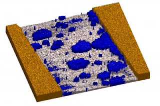
Caption: This is an Atomic Force Microscopy image of island growth in between two electrodes (left and right) of the SAMFET. The self-assembled monolayer islands, in the middle of the figure, conduct charges. In this case, no path is formed between the two electrodes and therefore current cannot flow. The height of the molecules is 3 nanometers; the length of the gap between the electrodes (i.e. the transistor channel length) is 5 microns.

Credit: Simon Mathijssen. Usage Restrictions: The image may only be used with appropriate caption and credit.
The SAMFET is a recent example of the development of 'plastic micro-electronics'- i.e. electronics based on organic materials. Last year, Philips Research managed to build such a transistor by immersing a silicon substrate into solution containing liquid crystalline molecules that self-assemble onto this substrate, resulting in a semi-conductive layer of just a single molecule thick. The monolayer of the SAMFET consists of molecules that are standing upright. Conduction takes place by charges jumping from one molecule to the other.

However, in previous attempts to make a SAMFET, it was observed that as the length of the SAMFET increased, its level of conductivity counterintuitively decreased exponentially.
In a joint project Philips Research, the Eindhoven University of Technology (TU/e), the University of Groningen, the Holst Centre, the Enikolopov Institute for Synthetical Polymer Materials in Moscow and the Technical University in Graz, Austria discovered that this decrease is determined by the monolayer coverage, which could be explained with a widely applicable two-dimensional percolation model.

The ultimate chemical sensor

One could compare this to crossing a river by jumping from rock to rock. The closer the rocks are to each other, the quicker one can jump or even walk to the other river bank. So if the monolayer displays more voids, the conductivity decreases dramatically. Up till now, this behavior was an uncharted area and inhibited the use of SAMFETs in applications such as sensors and plastic electronics. The SAMFET's extreme sensitivity could open doors to the development of the ultimate chemical sensor, the research team points out. "If we go back to that river again, another benefit of a SAMFET becomes clear", Martijn Kemerink, assistant professor at the TU/e indicates. "Imagine that there are just enough rocks to cross that river. When you remove just one rock, the effect is significant, for it is impossible to make it to the other side of the river. The SAMFET could be used to make sensors that give a large signal that is triggered by a small change", he continues.

Future steps

At present, SAMFETs are not widely used, for there are alternatives of which the production process is well-established. However, the production process of SAMFETs is extremely simple and material efficient. The transistor requires only a single layer of molecules that is applied by simple immersion into a chemical solution. The same solution can be used for many substrates, for the substrate only takes the necessary (small) amount of molecules. This makes future large-scale production of monolayer electronics efficient, simple and cost-effective. ###

Publication

The publication "Monolayer coverage and channel length set the mobility in self-assembled monolayer field-effect transistors", by Matthijssen et al. can be found at www.nature.com/nnano/journal/.

The research was conducted at Philips Research Eindhoven and Eindhoven University of Technology. It was funded by STW, ONE-P, the Austrian Nanoinitiative and H.C. Starck GmbH.

Contact: Simon Mathijssen s.g.j.mathijssen@tue.nl 31-065-336-1312 Eindhoven University of Technology

Friday, October 02, 2009

Nanoelectronic transistor combined with biological machine could lead to better electronics

LIVERMORE, Calif. -- If manmade devices could be combined with biological machines, laptops and other electronic devices could get a boost in operating efficiency.

Lawrence Livermore National Laboratory researchers have devised a versatile hybrid platform that uses lipid-coated nanowires to build prototype bionanoelectronic devices.

Mingling biological components in electronic circuits could enhance biosensing and diagnostic tools, advance neural prosthetics such as cochlear implants, and could even increase the efficiency of future computers.

bioanoelectronic device

An artist’s representation of a bioanoelectronic device incorporating alamethicin biological pore. In the core of the device is a silicon nanowire (grey), covered with a lipid bilayer (blue). The bilayer incorporates bundles of alamethicin molecules (purple) that form pore channels in the membrane. Transport of protons though these pore channels changes the current through the nanowire. Image by Scott Dougherty, LLNL
While modern communication devices rely on electric fields and currents to carry the flow of information, biological systems are much more complex. They use an arsenal of membrane receptors, channels and pumps to control signal transduction that is unmatched by even the most powerful computers. For example, conversion of sound waves into nerve impulses is a very complicated process, yet the human ear has no trouble performing it.

"Electronic circuits that use these complex biological components could become much more efficient," said Aleksandr Noy, the LLNL lead scientist on the project.

While earlier research has attempted to integrate biological systems with microelectronics, none have gotten to the point of seamless material-level incorporation.

"But with the creation of even smaller nanomaterials that are comparable to the size of biological molecules, we can integrate the systems at an even more localized level," Noy said.
To create the bionanoelectronic platform the LLNL team turned to lipid membranes, which are ubiquitous in biological cells. These membranes form a stable, self-healing,and virtually impenetrable barrier to ions and small molecules.

"That's not to mention that these lipid membranes also can house an unlimited number of protein machines that perform a large number of critical recognition, transport and signal transduction functions in the cell," said Nipun Misra, a UC Berkeley graduate student and a co-author on the paper.

Julio Martinez, a UC Davis graduate student and another co-author added: "Besides some preliminary work, using lipid membranes in nanoelectronic devices remains virtually untapped."

The researchers incorporated lipid bilayer membranes into silicon nanowire transistors by covering the nanowire with a continuous lipid bilayer shell that forms a barrier between the nanowire surface and solution species.

"This 'shielded wire' configuration allows us to use membrane pores as the only pathway for the ions to reach the nanowire," Noy said. "This is how we can use the nanowire device to monitor specific transport and also to control the membrane protein."

The team showed that by changing the gate voltage of the device, they can open and close the membrane pore electronically.

The research appears Aug. 10 in the online version of the Proceedings of the National Academy of Sciences. ###

Founded in 1952, Lawrence Livermore National Laboratory is a national security laboratory, with a mission to ensure national security and apply science and technology to the important issues of our time. Lawrence Livermore National Laboratory is managed by Lawrence Livermore National Security, LLC for the U.S. Department of Energy's National Nuclear Security Administration.

Contact: Anne Stark stark8@llnl.gov 925-422-9799 DOE/Lawrence Livermore National Laboratory