


New techniques pave way for carbon nanotubes in electronic devices
 | Troy, N.Y. -- Many of the vaunted applications of carbon nanotubes require the ability to attach these super-tiny cylinders to electrically conductive surfaces, but to date researchers have only been successful in creating high-resistance interfaces between nanotubes and substrates. |
The results, which appear in separate papers from the November issue of Nature Nanotechnology and the Oct. 16 issue of Applied Physics Letters (APL), could help overcome some of the key hurdles to using carbon nanotubes in computer chips, displays, sensors, and many other electronic devices.
"Carbon nanotubes offer promising applications in fields ranging from electronics to biotechnology," said Saikat Talapatra, a postdoctoral research associate with the Rensselaer Nanotechnology Center and lead author of the Nature Nanotechnology paper. But since many of these applications are based on the superior conductivity of carbon nanotubes, good contact between nanotubes and conducting metal components is essential.
Both of the newly developed techniques could bring the use of nanotubes as interconnects on computer chips closer to reality -- a long-sought goal in the nanotechnology community. As chip makers seek to continually increase computing power, they are looking to shrink the dimensions of chip components to the nanometer scale, or about 1-100 billionths of a meter. Communication between components becomes increasingly difficult at this incredibly small scale, making carbon nanotubes a natural choice to replace metal wires, according to the researchers.
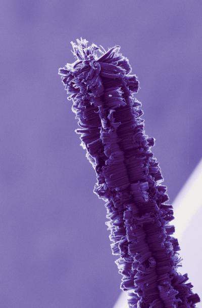
In the first technique -- dubbed "floating catalyst chemical vapor deposition" -- they heat a carbon-rich compound at extremely high temperatures until the material vaporizes. As the system cools, carbon deposits directly on the metal surface in the form of nanotube arrays. For this experiment, the team used surfaces made from Inconel, a nickel-based "super alloy" with good electrical conductivity. Until now this technique has only been used to grow nanotubes on substrates that are poor conductors of electricity.
There are many potential advantages to growing carbon nanotubes directly on metals with this simple, single-step process, according to Talapatra. Nanotubes attach to the surface with much greater strength; excellent electrical contact is established between the two materials; and nanotubes can be grown on surfaces of almost any shape and size, from curved sheets to long metal rods.
But chemical vapor deposition is a high-temperature process, which makes it incompatible with some sensitive electronic applications. "We have developed an alternate process of obtaining carbon nanotube arrays on any conducting substrate by contact printing methods," said Ashavani Kumar, a postdoctoral research associate in materials science and engineering at Rensselaer and lead author of the APL paper.
In collaboration with Rajashree Baskaran, a staff research engineer in the Components Research Division at Intel Corporation, the team developed a procedure that mimics the way photographs are printed from a film negative. They first grow patterns of carbon nanotubes on silicon surfaces using chemical vapor deposition, and then the nanotubes are transferred to metal surfaces that are coated with solder -- a metal alloy that is melted to join metallic surfaces together. The nanotubes stick in the solder, maintaining their original arrangement on the new surface.
And since solder has a low melting point, the process takes place at low temperature. "The contact printing process we have developed provides a potentially versatile method of incorporating carbon nanotubes in applications which cannot tolerate the typical high temperature of growth," Baskaran said.
In addition to showing promise for interconnects in computer chips, carbon nanotubes also exhibit a physical property called "field emission." When a voltage is applied, electrons are pulled out from the surface, which means that nanotubes could be combined with metals to produce high-resolution electronic displays, chemical sensors, and flash memory devices for computers.
The researchers also demonstrated that the chemical vapor deposition procedure can be used to make nanotube electrodes for "super capacitors" -- devices that have unusually high energy densities when compared to common capacitors, which are used to store energy in electrical circuits. These are of particular interest in automotive applications for hybrid vehicles and as supplementary storage for battery electric vehicles, according to the researchers. ###
The research published in Nature Nanotechnology was funded by the National Science Foundation and the Interconnect Focus Center. The APL work was funded by Intel Corporation via a gift grant.
Both projects were performed under the guidance of Pulickel Ajayan, the Henry Burlage Professor of Materials Science and Engineering at Rensselaer and a world-renowned expert in fabricating nanotube-based materials. Other Rensselaer researchers involved with the project are: Robert Vajtai, Swastik Kar, Omkaram Nalamasu, Victor Pushparaj, Sunil Pal, Lijie Ci, Mancheri Shaijumon, and Sumanjeet Kaur.
Nanotechnology at Rensselaer
In September 2001, the National Science Foundation selected Rensselaer as one of the six original sites for a new Nanoscale Science and Engineering Center (NSEC). As part of the U.S. National Nanotechnology Initiative, the program is housed within the Rensselaer Nanotechnology Center and forms a partnership between Rensselaer, the University of Illinois at Urbana-Champaign, and Los Alamos National Laboratory. The mission of Rensselaer's Center for Directed Assembly of Nanostructures is to integrate research, education, and technology dissemination, and to serve as a national resource for fundamental knowledge in directed assembly of nanostructures. The five other original NSECs are located at Harvard University, Columbia University, Cornell University, Northwestern University, and Rice University.
About Rensselaer: Rensselaer Polytechnic Institute, founded in 1824, is the nation's oldest technological university. The university offers bachelor's, master's, and doctoral degrees in engineering, the sciences, information technology, architecture, management, and the humanities and social sciences. Institute programs serve undergraduates, graduate students, and working professionals around the world. Rensselaer faculty are known for pre-eminence in research conducted in a wide range of fields, with particular emphasis in biotechnology, nanotechnology, information technology, and the media arts and technology. The Institute is well known for its success in the transfer of technology from the laboratory to the marketplace so that new discoveries and inventions benefit human life, protect the environment, and strengthen economic development.
Technorati Tags: nanofibers or Nanoscientists and Nano or Nanotechnology and nanoparticles or Nanotech and nanotubes or nanochemistry and nanoscale or nanowires and Nanocantilevers or nanometrology and nanostructure or floating catalyst chemical vapor deposition and Rensselaer Polytechnic Institute or electronic devices
Contact: Jason Gorss gorssj@rpi.edu 518-276-6098 Rensselaer Polytechnic Institute


No comments:
Post a Comment