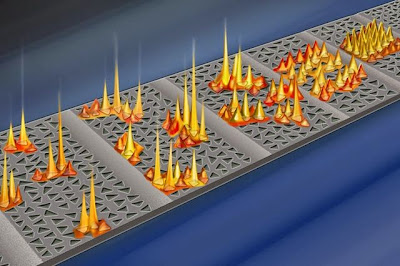
Exotic states materialize with supercomputers. Materials with novel electrical properties discovered using XSEDE computational resources Stampede and Lonestar supercomputers of TACC
UNIVERSITY OF TEXAS AT AUSTIN, TEXAS ADVANCED COMPUTING CENTER
The science team included Ju Li, Liang Fu, Xiaofeng Qian, and Junwei Liu, experts in topological phases of matter and two-dimensional materials research at the Massachusetts Institute of Technology (MIT). They calculated the electronic structures of the materials using the Stampede and Lonestar supercomputers of the Texas Advanced Computing Center.
The computational allocation was made through XSEDE, the Extreme Science and Engineering Discovery Environment, a single virtual system funded by the National Science Foundation (NSF) that scientists use to interactively share computing resources, data and expertise. The study was funded by the U.S. Department of Energy and the NSF.

This picture tells quite a story to scientists. It's a portrait of what they call a topological insulator, materials that conduct only at their edges. Technically it shows the edge density of states calculated for a monolayer transition metal dichalcogenide in the 1T'-MoS2 structural phase.
There's a black gap between the purple blobs at the bottom and top. What's more, there's crisscrossing reddish lines that bridge the gap. The lines indicate the edge state of the material, allowing electrons to cross the gap and conduct electricity. CREDIT: (Credit: Qian et. al.) USAGE RESTRICTIONS: None
"To me, national computing resources like XSEDE, or specifically the Stampede and Lonestar supercomputers, are extremely helpful to computational scientists," Xiaofeng Qian said. In January 2015, Qian left MIT to join Texas A&M University as the first tenure-track assistant professor at its newly formed Department of Materials Science and Engineering.
What Qian and colleagues did was purely theoretical work, using Stampede for part of the calculations that modeled the interactions of atoms in the novel materials, two-dimensional transition metal dichalcogenides (TMDC). Qian used the molecular dynamics simulation software Vienna Ab initio Simulation Package to model a unit cell of atoms, the basic building block of the crystal lattice of TMDC.
"If you look at the unit cell, it's not large. They are just a few atoms. However, the problem is that we need to predict the band structure of charge carriers in their excited states in the presence of spin-orbit coupling as accurately as possible," Qian said.
Scientists diagram the electronic band structure of materials to show the energy ranges an electron is allowed, with the band gap showing forbidden zones that basically block the flow of current. Spin-orbit coupling accounts for the electromagnetic interactions between electron's spin and magnetic field generated from the electron's motion around the nucleus.
"We found a very convenient method to control the topological phase transition in these quantum spin Hall interlayers."
Xiaofeng Qian, Assistant Professor in the Department of Materials Science and Engineering at Texas A&M University.
The complexity lies in the details of these interactions, for which Qian applied many-body perturbation theory with the GW approximation, a state-of-the-art first principles method, to calculate the quasiparticle electronic structures for electrons and holes. The 'G' is short for Green's Function and 'W' for screened Coulomb interaction, Qian explained.
"In order to carry out these calculations to obtain reasonable convergence in the results, we have to use 96 cores, sometimes even more," Qian said. "And then we need them for 24 hours. The Stampede computer is very efficient and powerful. The work that we have been showing is not just one material; we have several other materials as well as different conditions. In this sense, access to the resources, especially Stampede, is very helpful to our project."
The big picture for Qian and his colleagues is the hunt for new kinds of materials with extraordinarily useful properties. Their target is room-temperature quantum spin Hall insulators, which are basically near-two-dimensional materials that block current flow everywhere except along their edges. "Along the edges you have the so-called spin up electron flow in one direction, and at the same time you have spin down electrons and flows away in the opposite direction," Qian explained. "Basically, you can imagine, by controlling the injection of charge carriers, one can come up with spintronics, or electronics."
The scientists in this work proposed a topological field-effect transistor, made of sheets of hexagonal boron interlaced with sheets of TMDC. "We found a very convenient method to control the topological phase transition in these quantum spin Hall interlayers," Qian said. "This is very important because once we have this capability to control the phase transition, we can design some electronic devices that can be controlled easily through electrical fields."
Media Contact: Faith Singer-Villalobos faith@tacc.utexas.edu 512-232-5771
Quantum spin Hall effect in two-dimensional transition metal dichalcogenides. More about this image and story at Nanotechnology Today - http://nanotechnologytoday.blogspot.com/2015/03/quantum-spin-hall-effect-in-two.html
Exotic states materialize with supercomputers. Materials with novel electrical properties discovered using XSEDE computational resources Stampede and Lonestar supercomputers of TACC.
Scientists used supercomputers to find a new class of materials that possess an exotic state of matter known as the quantum spin Hall effect. The researchers published their results in the journal Science in December 2014, where they propose a new type of transistor made from these materials.


