Friday, September 30, 2011

Rensselaer Polytechnic Institute researchers 'cook' promising new heat-harvesting nanomaterials in microwave oven

Rensselaer Polytechnic Institute researchers create large marble-sized pellets of thermoelectric nanomaterials

Troy, N.Y. – Waste heat is a byproduct of nearly all electrical devices and industrial processes, from driving a car to flying an aircraft or operating a power plant. Engineering researchers at Rensselaer Polytechnic Institute have developed new nanomaterials that could lead to techniques for better capturing and putting this waste heat to work. The key ingredients for making marble-sized pellets of the new material are aluminum and a common, everyday microwave oven.

Harvesting electricity from waste heat requires a material that is good at conducting electricity but poor at conducting heat. One of the most promising candidates for this job is zinc oxide, a nontoxic, inexpensive material with a high melting point. While nanoengineering techniques exist for boosting the electrical conductivity of zinc oxide, the material's high thermal conductivity is a roadblock to its effectiveness in collecting and converting waste heat. Because thermal and electrical conductivity are related properties, it's very difficult to decrease one without also diminishing the other.

However, a team of researchers led by Ganpati Ramanath, professor in the Department of Materials Science and Engineering at Rensselaer, in collaboration with the University of Wollongong, Australia, have demonstrated a new way to decrease zinc oxide's thermal conductivity without reducing its electrical conductivity.

Heat-Harvesting Nanomaterials in Microwave Oven

Heat-Harvesting Nanomaterials in Microwave Oven
The innovation involves adding minute amounts of aluminum to zinc oxide, and processing the materials in a microwave oven. The process is adapted from a technique invented at Rensselaer by Ramanath, graduate student Rutvik Mehta, and Theo Borca-Tasciuc, associate professor in the Department of Mechanical, Aerospace, and Nuclear Engineering (MANE). This work could open the door to new technologies for harvesting waste heat and creating highly energy efficient cars, aircraft, power plants, and other systems.

"Harvesting waste heat is a very attractive proposition, since we can convert the heat into electricity and use it to power a device—like in a car or a jet—that is creating the heat in the first place. This would lead to greater efficiency in nearly everything we do and, ultimately, reduce our dependence on fossil fuels," Ramanath said.

"We are the first to demonstrate such favorable thermoelectric properties in bulk-sized high-temperature materials, and we feel that our discovery will pave the way to new power harvesting devices from waste heat."

Results of the study are detailed in the paper "Al-Doped Zinc Oxide Nanocomposites with Enhanced Thermoelectric Properties," published recently by the journal Nano Letters. View the paper online at: http://pubs.acs.org/doi/abs/10.1021/nl202439h

To create the new nanomaterial, researchers added minute quantities of aluminum to shape-controlled zinc oxide nanocrystals, and heated them in a $40 microwave oven. Ramanath's team is able to produce several grams of the nanomaterial in a matter of few minutes, which is enough to make a device measuring a few centimeters long. The process is less expensive and more scalable than conventional methods and is environmentally friendly, Ramanath said. Unlike many nanomaterials that are fabricated directly onto a substrate or surface, this new microwave method can produce pellets of nanomaterials that can be applied to different surfaces. These attributes, together with low thermal conductivity and high electrical conductivity, are highly suitable for heat harvesting applications.

"Our discovery could be key to overcoming major fundamental challenges related to working with thermoelectric materials," said project collaborator Borca-Tasciuc. "Moreover, our process is amenable to scaling for large-scale production. It's really amazing that a few atoms of aluminum can conspire to give us thermoelectric properties we're interested in."

###

This work was a collaborative effort between Ramanath and Shi Xue Dou, a professor at the Institute for Superconducting and Electronic Materials at the University of Wollogong, Australia. Wollongong graduate student Priyanka Jood carried out the work together with Rensselaer graduate students Rutvik Mehta and Yanliang Zhang during Jood's one-year visit to Rensselaer. Co-authors of the paper are Richard W. Siegel, the Robert W. Hunt Professor of Materials Science and Engineering; along with professors Xiaolin Wang and Germanas Peleckis at the University of Wollongong.

This research is funded by support from IBM through the Rensselaer Nanotechnology Center; S3TEC, an Energy Frontier Research Center funded by the U.S. Department of Energy (DoE) Office of Basic Energy Sciences; the Australian Research Council (ARC); and the University of Wollongong.

For more information on Ramanath's research at Rensselaer, visit:

Contact: Michael Mullaney mullam@rpi.edu 518-276-6161 Rensselaer Polytechnic Institute

Wednesday, September 28, 2011

Semiconductor makers are also hoping diamonds will pan out as key components of long-lasting micromachines

Diamonds may be best known as a symbol of long-lasting love. But semiconductor makers are also hoping they'll pan out as key components of long-lasting micromachines if a new method developed at the National Institute of Standards and Technology (NIST) for carving these tough, capable crystals proves its worth.* The method offers a precise way to engineer microscopic cuts in a diamond surface, yielding potential benefits in both measurement and technological fields.

By combining their own observations with background gleaned from materials science, NIST semiconductor researchers have found a way to create unique features in diamond—potentially leading to improvements in nanometrology in short order, as it has allowed the team to make holes of precise shape in one of the hardest known substances. But beyond the creation of virtually indestructible nanorulers, the method could one day lead to the improvement of a class of electronic devices useful in cell phones, gyroscopes and medical implants.

Well known for making the hugely complex electronic microchips that run our laptops, the semiconductor industry has expanded its portfolio by fabricating tiny devices with moving parts. Constructed with substantially the same techniques as the electronic chips, these "micro-electromechanical systems," or MEMS, are just a few micrometers in size. They can detect environmental changes such as heat, pressure and acceleration, potentially enabling them to form the basis of tiny sensors and actuators for a host of new devices. But designers must take care that tiny moving parts do not grind to a disastrous halt. One way to make the sliding parts last longer without breaking down is to make them from a tougher material than silicon.

NIST Polishes Method for Creating Tiny Diamond Machines

Caption: This colorized electron microscope image reveals the boxy shape of the pits the NIST team etched into the diamond surface, exhibiting their smooth vertical sidewalls and flat bottom. The pits were between 1 and 72 micrometers in size.

Credit: NIST. Usage Restrictions: None.
"Diamond may be the ideal substance for MEMS devices," says NIST's Craig McGray. "It can withstand extreme conditions, plus it's able to vibrate at the very high frequencies that new consumer electronics demand. But it's very hard, of course, and there hasn't been a way to engineer it very precisely at small scales. We think our method can accomplish that."

The method uses a chemical etching process to create cavities in the diamond surface. The cubic shape of a diamond crystal can be sliced in several ways—a fact jewelers take advantage of when creating facets on gemstones. The speed of the etching process depends on the orientation of the slice, occurring at a far slower rate in the direction of the cube's "faces"—think of chopping the cube into smaller cubes—and these face planes can be used as a sort of boundary where etching can be made to stop when desired. In their initial experiments, the team created cavities ranging in width from 1 to 72 micrometers, each with smooth vertical sidewalls and a flat bottom.

"We'd like to figure out how to optimize control of this process next," McGray says, "but some of the ways diamond behaved under the conditions we used were unexpected. We plan to explore some of these mysteries while we develop a prototype diamond MEMS device."

###

* C.D. McGray, R.A. Allen, M. Cangemi and J. Geist. Rectangular scale-similar etch pits in monocrystalline diamond. Diamond and Related Materials. Available online 22 August 2011, ISSN 0925-9635, 10.1016/j.diamond.2011.08.007.

Contact: Chad Boutin boutin@nist.gov 301-975-4261 National Institute of Standards and Technology (NIST)

Monday, September 26, 2011

New approach could allow the electronics industry to drastically reduce power consumption and increase speed in the next generation of computers

RIVERSIDE, Calif. (www.ucr.edu) -- Two professors from the University of California, Riverside’s Bourns College of Engineering have received $1.5 million to study a new approach that could allow the electronics industry to drastically reduce power consumption and increase speed in the next generation of computers.

Alexander Balandin, a professor of electrical engineering and chair of the materials science and engineering program, and Roger Lake, a professor of electrical engineering, will work with John Stickney, a professor of chemistry at the University of Georgia. Balandin serves as a principal investigator for the overall project, coordinating experimental research in his laboratory with computational studies in Lake’s group and materials growth activities in Stickney’s group.

The money is awarded under the nation-wide Nanoelectronics for 2020 and Beyond competition. The researchers will receive $1.3 million in funding from the National Science Foundation and $200,000, as a gift, from the Nanoelectronics Research Initiative of the Semiconductor Research Corporation, a technology research consortium whose members include Intel, IBM and other high-tech leaders.

For 50 years, electronics have run on silicon transistor technology. Over those years, that technology has continually been scaled down to the point now further shrinkage is difficult. Continuing evolution of electronics beyond the limits of the conventional silicon technology requires innovative approaches for solving heat dissipation, speed and scaling issues.

Alex Balandin

Alex Balandin, a professor of electrical engineering and chair of the materials science and engineering program
Balandin and Lake believe they have found that innovative approach.

They plan to encode information not with conventional electrical currents, individual charges or spins but with the collective states formed by the charge-density waves.

Charge-density waves, also known as CDWs, are modulations in the electron density and associated modulations of the atom positions in crystal lattices of certain materials. They were known for almost a century but until today have not been considered for applications in computing. The use of collective states, or waves, instead of electrical currents of individual electrons can help to reduce the amount of power needed per computation.

“The idea of using charge-density waves for information processing is a bold one and presents an absolutely new approach for solving the scaling and heat dissipation problems in electronics,” said Balandin, who received this year’s Pioneer of Nanotechnology Award from the IEEE Nanotechnology Council.

The research to be carried out at UC Riverside will complement conventional silicon transistor technology. The charge-density wave materials can be integrated with silicon and other materials used in conventional computers. The prototype devices, which use the charge-density waves, have already been built in Balandin’s Nano-Device Laboratory.

The phase, frequency and amplitude of the collective current of the interfering charge waves will encode information and allow for massive parallelism in information processing. The low-dissipation, massively parallel information processing with the collective state variables can satisfy the computational, communication, and sensor technology requirements for decades to come.

The paradigm proposed by Balandin and Lake has never been attempted before. Its major benefit is that it can be implemented at room temperature and does not require magnetic fields like other computational schemes do.

The project will lead to better understanding of the material properties and physical processes of charge-density wave materials in highly-scaled, low-dimension regimes that have not yet been explored. Among the outcomes of this research will be optimized device designs for exploiting charge-density waves for computations and understanding the fundamental limits of the performance metrics.

The University of California, Riverside (www.ucr.edu) is a doctoral research university, a living laboratory for groundbreaking exploration of issues critical to Inland Southern California, the state and communities around the world. Reflecting California's diverse culture, UCR's enrollment has exceeded 20,500 students. The campus will open a medical school in 2013 and has reached the heart of the Coachella Valley by way of the UCR Palm Desert Graduate Center. The campus has an annual statewide economic impact of more than $1 billion.

A broadcast studio with fiber cable to the AT&T Hollywood hub is available for live or taped interviews. UCR also has ISDN for radio interviews. To learn more, call (951) UCR-NEWS.

Contact: Sean Nealon sean.nealon@ucr.edu 951-827-1287 University of California - Riverside

Saturday, September 24, 2011

Simple nanoantenna that directs red and blue colours in opposite directions

Researchers at Chalmers University of Technology have built a very simple nanoantenna that directs red and blue colours in opposite directions, even though the antenna is smaller than the wavelength of light. The findings – published in the online journal Nature Communications this week – can lead to optical nanosensors being able to detect very low concentrations of gases or biomolecules.
A structure that is smaller than the wavelength of visible light (390-770 nanometers) should not really be able to scatter light. But that is exactly what the new nanoantenna does. The trick employed by the Chalmers researchers is to build an antenna with an asymmetric material composition, creating optical phase shifts.

The antenna consists of two nanoparticles about 20 nanometers apart on a glass surface, one of silver and one of gold. Experiments show that the antenna scatters visible light so that red and blue colours are directed in opposite directions.

“The explanation for this exotic phenomenon is optical phase shifts,” says Timur Shegai, one of the researchers behind the discovery. “The reason is that nanoparticles of gold and silver have different optical properties, in particular different plasmon resonances. Plasmon resonance means that the free electrons of the nanoparticles oscillate strongly in pace with the frequency of the light, which in turn affects the light propagation even though the antenna is so small. “

nanoantenna

The nanoantenna acts as a router for red and blue light, due to the nanoparticles of gold and silver having different optical properties. Image: Timur Shegai
The method used by the Chalmers researchers to control the light by using asymmetric material composition – such as silver and gold – is completely new. It is easy to build this kind of nanoantenna; the researchers have shown that the antennas can be fabricated densely over large areas using cheap colloidal lithography.

The research field of nanoplasmonics is a rapidly growing area, and concerns controlling how visible light behaves at the nanoscale using a variety of metal nanostructures. Scientists now have a whole new parameter – asymmetric material composition – to explore in order to control the light.

Nanoplasmonics can be applied in a variety of areas, says Mikael Käll, professor in the research group at Chalmers.

“One example is optical sensors, where you can use plasmons to build sensors which are so sensitive that they can detect much lower concentrations of toxins or signalling substances than is possible today. This may involve the detection of single molecules in a sample, for example, to diagnose diseases at an early stage, which facilitates quick initiation of treatment.”

The results were presented at an international conference on optical nanosensors at Chalmers this week. Chalmers is one of the leading universities in nanoplasmonic biosensors, and 130 scientists from around the world are attending the conference.

The research has received financial support from the Swedish Foundation for Strategic Research, the Swedish Research Council and the Göran Gustafsson Foundation.

For more information, please contact: Timur Shegai, PhD, bionanophotonics, +46 31 772 31 23, timurs@chalmers.se Mikael Käll, Professor, bionanophotonics, +46 31 772 31 19, mikael.kall@chalmers.se

Contact: Christian Borg press@chalmers.se 46-317-723-395 Swedish Research Council

Wednesday, September 21, 2011

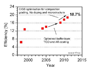
Flexible CIGS solar cells with an 18.7% world record efficiency developed

The technology yielding flexible solar cells with an 18.7% world record efficiency developed by scientists at Empa, the Swiss Federal Laboratories for Materials Science and Technology, has now been published in “Nature Materials”. Key to the breakthrough is the control of the energy band gap grading in the copper indium gallium (di)selenide semiconductor, also known as CIGS, the layer that absorbs light and converts it into electricity.

High-performance flexible and lightweight solar cells, say, on plastic foils, have excellent potential to lower the manufacturing costs through roll-to-roll processing and the so called “balance-of-system” cost, thus enabling affordable solar electricity in the near future. Thus far, however, flexible solar cells on polymer films have been lacking behind in performance compared to rigid cells, primarily because polymer films require much lower temperatures during deposition of the absorber layer, generally resulting in much lower efficiencies.

Record-breaking team

The research team at Empa's Laboratory for Thin Film and Photovoltaics, led by Ayodhya N. Tiwari, has been involved in the development of high-efficiency CIGS solar cells on both glass and flexible substrates with a special focus on reducing the deposition temperature of the CIGS layer. The group has repeatedly increased efficiency of flexible CIGS solar cells over the past years – first at ETH Zurich and now since three years at Empa. With their current record value of 18.7% Tiwari and his team nearly closed the efficiency gap to cells based on multi-crystalline silicon (Si) wafers or CIGS cells on glass. The scientific details of their novel low-temperature deposition technology and the multi-layered device have recently been published in “Nature Materials”.

Flexible CIGS solar cells

Flexible CIGS solar cells developed at Empa.

flexible CIGS solar cells

Improvement in energy conversion efficiency of flexible CIGS solar cells on polymer film lead to the world record efficiency of 18.7% for flexible CIGS solar cells developed at Empa.
“To achieve such high efficiency values, we had to reduce the recombination losses of photo-generated charge carriers”, said Tiwari. CIGS layers grown by co-evaporation at temperature of around 450 °C have a strong composition grading because of inadequate inter-diffusion of intermediate phases and preferential diffusion of gallium (Ga) towards the electrical back contact
To overcome this problem doctoral students Adrian Chiriḷ and Patrick Bloesch developed novel processes for optimizing the solar cell performance. To achieve an appropriate composition profile in the CIGS layer Рfor enabling more efficient charge carrier collection and reduced interface recombination РChiriḷ and colleagues developed an innovative growth process by carefully controlling the Ga and indium (In) evaporation flux during different stages of the evaporation process.

High-efficiency solar cells – grown on cheap metal-foils

Such high-efficiency CIGS solar cells up to now were developed only on glass substrates with processes where CIGS layers are grown at temperatures of 600 °C or above. In contrast, polymer foils cannot withstand such high temperatures.

The low-temperature process now developed by Tiwari and Co. not only yielded an 18.7%-efficiency cell on polymer foils but also another record efficiency of 17.7% on steel foil without any diffusion oxide or nitride barrier layer commonly used in high-temperature processes.

Both efficiencies were independently certified by the Fraunhofer Institute for Solar Energy Systems (ISE) in Freiburg, Germany. “We have thus shown that this low-temperature process is also applicable on low-cost metal foils such as aluminum or Mild-steel, achieving comparably high-efficiency cells and indicating a severe cost reduction potential with this technology”, said Tiwari.

Scientists at FLISOM, a start-up company, and Empa have been collaborating to further develop low-temperature processing, and FLISOM is scaling up the technology for roll-to-roll manufacturing of monolithically interconnected solar modules and commercializing the technology. The research has been supported by the Swiss National Science Foundation (SNSF), the Commission for Technology and Innovation (CTI), the Swiss Federal Office of Energy (SFOE), EU Framework Programmes as well as by Swiss companies W. Blösch AG and FLISOM.

Further Information: Prof. Dr. Ayodhya N. Tiwari, Thin Film and Photovoltaics, Tel. +41 58 765 41 30 ayodhya.tiwari@empa.ch

Editor / Media contact, Dr. Michael Hagmann, Communication Dept. Tel. +41 58 765 45 92 redaktion@empa.ch

Monday, September 19, 2011

Researchers at UC Santa Barbara has developed a breakthrough technology that can be used to discriminate cancerous prostate cells

(Santa Barbara, Calif.) –– A team of researchers at UC Santa Barbara has developed a breakthrough technology that can be used to discriminate cancerous prostate cells in bodily fluids from those that are healthy. The findings are published this week in the Proceedings of the National Academy of Sciences.

While the new technology is years away from use in a clinical setting, the researchers are nonetheless confident that it will be useful in developing a microdevice that will help in understanding when prostate cancer will metastasize, or spread to other parts of the body.

"There have been studies to find the relationship between the number of cancer cells in the blood, and the outcome of the disease," said first author Alessia Pallaoro, postdoctoral fellow in UCSB's Department of Chemistry and Biochemistry. "The higher the number of cancer cells there are in the patient's blood, the worse the prognosis.

"The cancer cells that are found in the blood are thought to be the initiators of metastasis," Pallaoro added. "It would be really important to be able to find them and recognize them within blood or other bodily fluids. This could be helpful for diagnosis and follow-ups during treatment."

Cancerous and Non-cancerous Cells are Incubated with Silver Nanoparticle Biotags

Caption: Cancerous and non-cancerous cells are incubated with silver nanoparticle biotags, and then analyzed by shining the red laser on them. The biotags are shown on the cells' surface. Those glowing red in the middle are the cancer biomarkers, and those glowing green are standard biomarkers that bind to many cell types. A high ratio of red to green is found on the cancer cells.

Credit: Gary Braun and Peter Allen / UCSB. Usage Restrictions: None

Cells Shown in the Image are Cancerous

Caption: Cells shown in the image are cancerous. The simple color code makes visual identification easy. Red indicates the cancer biomarkers.

Credit: Alessia Pallaoro/UCSB. Usage Restrictions: None
The researchers explained that although the primary tumor does not kill prostate cancer patients, metastasis does. "The delay is not well understood," said Gary Braun, second author and postdoctoral fellow in the Department of Molecular, Cellular, and Developmental Biology. "There is a big focus on understanding what causes the tumor to shed cells into the blood. If you could catch them all, then you could stop metastasis. The first thing is to monitor their appearance."

The team developed a novel technique to discriminate between cancerous and non-cancerous cells using a type of laser spectroscopy called surface enhanced Raman spectroscopy (SERS) and silver nanoparticles, which are biotags.

"Silver nanoparticles emit a rich set of colors when they absorb the laser light," said Braun. "This is different than fluorescence. This new technology could be more powerful than fluorescence."

The breakthrough is in being able to include more markers in order to identify and study unique tumor cells that are different from the main tumor cells, explained Pallaoro. "These different cells must be strong enough to start a new tumor, or they must develop changes that allow them to colonize in other areas of the body," she said. "Some changes must be on the surface, which is what we are trying to detect."

The team is working to translate the technology into a diagnostic microdevice for studying cancer cells in the blood. Cells would be mixed with nanoparticles and passed through a laser, then discriminated by the ratio of two signals.


The two types of biotags used in this research have a particular affinity that is dictated by the peptide they carry on their surface. One type attaches to a cell receptor called neuropilin-1, a recently described biomarker found on the surface membrane of certain cancer cells.

The other biotag binds many cell types (both cancerous and non-cancerous) and serves as a standard measure as the cells are analyzed.

In this study, the team mixed the two biotags and added them to the healthy and tumor cell cultures. The average SERS signal over a given cell image yielded a ratio of the two signals consistent with the cells' known identity.

Pallaoro said she believes the most important part of the new technique is the fact that it could be expanded by adding more colors –– different particles of different colors –– as more biomarkers are found. The team used a new biomarker discovered by scientists at UCSB and the Sanford Burnham Medical Research Institute.

###

The senior author of the paper is Martin Moskovits, professor in UCSB's Department of Chemistry and Biochemistry.

Contact: Gail Gallessich gail.g@ia.ucsb.edu 805-893-7220 University of California - Santa Barbara

Saturday, September 17, 2011

Research could enable advances such as invisibility cloaks, nanoscale lasers, high-efficiency lighting, and quantum computers

ANN ARBOR, Mich.---A new $13-million National Science Foundation center based at the University of Michigan will develop high-tech materials that manipulate light in new ways. The research could enable advances such as invisibility cloaks, nanoscale lasers, high-efficiency lighting, and quantum computers.

The Center for Photonic and Multiscale Nanomaterials, dubbed C-PHOM, involves engineering and physics researchers from the U-M College of Engineering and the College of Literature, Science, and the Arts, as well as close collaborators at Purdue University and several other institutions.

Photonics is the study and use of light to transmit and store information, as well as to image things humans can't see with unaided eyes. It's one of the key technologies underlying modern life, says Ted Norris, director of the new center and a U-M professor in the Department of Electrical Engineering and Computer Science.

Photonics provides the high-speed backbone of the Internet through fiber optics. It serves as a ubiquitous tool for medical imaging. And it enables the study of the most exotic ideas in quantum physics, such as entanglement and quantum computing.

"Advances in photonics depend critically on new materials, and this new center brings together top minds in electrical engineering, materials science, and physics to focus on two of the most exciting new directions in materials for nanophotonics," Norris said. "The cross-campus collaboration will enable fundamental advances."

sub-wavelength focussing of light

An illustration of the sub-wavelength focussing of light by a so-called "near-field plate," a device made of a metamaterial that was invented by physics professor Roberto Merlin and co-developed by electrical engineering associate professor Anthony Grbic.
Credit: Roberto Merlin.

The center has two thrusts. One group will focus on improving "wide bandgap semiconductors" such as gallium nitride, which could make possible quantum emitters that release one photon, or light particle, at a time and could advance quantum computing and quantum information processing.

Quantum computers could vastly improve computer security. Because they could theoretically factor numbers dramatically faster than conventional computers, they could allow for the creation of foolproof security codes. This research thrust also has applications in high-efficiency lighting and imaging. Leading this group is Pallab Bhattacharya, the Charles M. Vest Distinguished University Professor, and a professor in the U-M Department of Electrical Engineering and Computer Science.

A second group of researchers will develop better metamaterials, uniquely engineered mixtures of substances that enable scientists to make light act in ways it does not behave in nature. For example, metamaterials make it possible to focus light to a speck smaller than its wavelength, They could potentially be used to bend light around objects, making them invisible. They could also bring about "ultra subwavelength imaging" to see inside biological cells with unprecedented resolution. Leading this group is Roberto Merlin, the Peter A. Franken Collegiate Professor of Physics at U-M. His team will work in close collaboration with researchers at Purdue.

The center will be located in the U-M Engineering Research Building on North Campus.

###

Other institutions involved in the new center are: Wayne State University, the City University of New York's Queens College, the University of Texas at Austin, the University of Illinois at Urbana-Champagne, and Argonne and Sandia national laboratories.

For more information:

Ted Norris: www.engin.umich.edu/research/cuos/ResearchGroups/US/

Pallab Bhattacharya: www.eecs.umich.edu/eecs/etc/fac/facsearchform

Roberto Merlin: www-personal.umich.edu/~merlin/

Contact: Nicole Casal Moore ncmoore@umich.edu 734-647-7087 University of Michigan

Thursday, September 15, 2011

Nanotechnology sensor could lead to earlier diagnosis for world's deadliest form of cancer

Researchers Unveil Method for Detecting Lung Cancer in Nature Article

Nanotechnology sensor could lead to earlier diagnosis for world's deadliest form of cancer

When lung cancer strikes, it often spreads silently into more advanced stages before being detected. In a new article published in Nature Nanotechnology, biological engineers and medical scientists at the University of Missouri reveal how their discovery could provide a much earlier warning signal.

"Early detection can save lives, but there is currently no proven screening test available for lung cancer," said Michael Wang, MD, PhD, assistant professor of pathology and anatomical sciences at MU and a corresponding author for the article. "We've developed highly sensitive technology that can detect a specific molecule type in the bloodstream when lung cancer is present."

Worldwide and in the United States, lung cancer is the most common cause of cancer-related death. In the U.S., more than 221,000 people will be newly diagnosed with lung cancer in 2011, and more than 155,000 people will die from the disease this year.

Michael Wang, Li-Qun Gu

Michael Wang, MD, PhD, right, assistant professor of pathology and anatomical sciences, and Li-Qun Gu, PhD, associate professor of biological engineering, have developed a new technology for the early detection of lung cancer. Worldwide and in the United States, lung cancer is the most common cause of cancer-related death.

MU researchers used blood plasma samples to detect a change in a specific small ribonucleic acid (microRNA) molecule that is often elevated in lung cancer patients. The scientists put an extract of blood plasma through a protein-based nanopore, which is a tiny hole in a thin membrane that is just big enough for a single molecule to pass through. By applying an ionic current to the nanopore, the scientists measured changes in the current that occur when the microRNA molecule associated with lung cancer is present.

"That altered current acts as a signal or bio-signature that is related to lung cancer," said Li-Qun Gu, PhD, an associate professor of biological engineering at MU and a corresponding author for the article. "Our new nanopore sensor is selective and sensitive enough to detect microRNAs at the single molecular level in plasma samples from lung cancer patients.

"While there are many research labs that focus on nanopore applications, this is the first time that nanopore technology has been used to detect lung cancer," Gu added. "This technology could possibly be used in the future to detect other cancer types as well as other types of diseases with specific DNA or RNA in the blood."

MU research published in the article was partially supported by grants from the National Science Foundation, National Institutes of Health and University of Missouri Intellectual Property Fast Track Initiative. The authors are associated with MU's College of Engineering, School of Medicine, Ellis Fischel Cancer Center and Dalton Cardiovascular Research Center.

Monday, September 12, 2011

Rensselaer Researchers Receive $2.65 Million NSF Grant To Install Balanced, Green Supercomputer at CCNI Supercomputing Center

Rensselaer Researchers Receive $2.65 Million NSF Grant To Install Balanced, Green Supercomputer at CCNI Supercomputing Center

A new system to be installed at the Rensselaer Polytechnic Institute supercomputing center will enable exciting new research possibilities across the nation and boost the university’s international leadership in computational modeling and simulation, data science, high-performance computing, and web science.

Funded by a $2.65 million grant from the National Science Foundation (NSF) and with additional support from Rensselaer and its Computational Center for Nanotechnology Innovations (CCNI), the new system will be a national resource for researchers in academia and industry across a wide range of disciplines. The system, scheduled to be delivered and installed in 2012, provides a balanced combination of computational power, fast data access, and visualization capabilities. It will be comprised of a powerful IBM Blue Gene/Q supercomputer, along with a multiterabyte memory (RAM) storage accelerator, petascale disk storage, rendering cluster, and remote display wall systems.

“The IBM Blue Gene/Q system is brand new, and should enable unprecedented innovations in massively parallel computing for data-intensive and multiscale research,” said Christopher Carothers, professor in the Department of Computer Science at Rensselaer, and lead researcher on the new grant. “Many important research projects are hitting a bottleneck, as the amount of data they’re generating continues to grow, as does their need to interact with this data. With our new balanced system, paired with the expertise of Rensselaer faculty and students, we should be able to help researchers in academia and industry to overcome many of these challenges.”

Christopher Carothers

Christopher Carothers, professor in the Department of Computer Science at Rensselaer.
“Congratulations to Rensselaer for this National Science Foundation award, which will help further cutting-edge research possibilities through the new IBM Blue Gene/Q supercomputer,” said U.S. Representative Paul Tonko. “This is an important partnership that helps provide Rensselaer with the tools that will help push critically needed research projects forward while educating students who will be the innovators and technology leaders of the future.”

The new supercomputer will be housed in CCNI, with visualization workstations and a display wall on the Rensselaer campus in the Curtis R. Priem Experimental Media and Performing Arts Center (EMPAC). The new Blue Gene/Q component of the system will have more computational power than the combined Blue Gene/L racks currently installed at CCNI, while taking up less than 1/30 of the space and using only 1/6 of the electrical power to operate. However, the true power of the new machine is in its balance: it will be many times faster than CCNI’s current system on data-intensive problems, and the combination of computation, fast data access, and visualization will support a significantly broader scope of research.

At Rensselaer, many research projects are poised to benefit from the new system. These projects include developing new methods for the diagnosis of breast cancer using data from non-invasive techniques; modeling plasmas to aid the design and safety of future fusion reactors; modeling wind turbine design to increase efficiencies and reduce maintenance; application of new knowledge discovery algorithms to very large semantic graphs for climate change and biomedical research, modeling heat flow in the world’s oceans, integrating data and computations across scales to gain a better understanding of biological systems and improve health care; and many others.

Time on the new system will be available to researchers nationwide. An allocation committee will be formed to assess proposals, on the basis of scientific merit, fit to the machine’s capabilities, and the potential to broaden the system’s user community and range of research. Rensselaer scientists and engineers also anticipate collaborations that will develop and apply the new techniques that will help researchers take advantage of this machine’s unique capabilities.

“Researchers at Rensselaer have developed highly scalable techniques that allow modeling to be done across hundreds of thousands of processors. This machine will further that research and provide a platform to explore new techniques that will be broadly applicable to exascale computing,” said Mark Shephard, professor in the department of Mechanical, Aerospace, and Nuclear Engineering (MANE) and director of the Scientific Computation Research Center at Rensselaer.

Experts in academia and industry anticipate realizing exascale computing — performing 1018 calculations per second — by the end of the decade. Exascale machines will be more than 100 times the computational power of today’s largest machines. The new Blue Gene/Q system at Rensselaer will be a first stop for many researchers looking to scale up their research over the next decade. Once researchers prove their project works on this system, they will well positioned to migrate to peta- and eventually exascale systems, including the large Blue Gene/Q systems due to be installed next year at two national laboratories.

Rensselaer faculty and students will benefit greatly by working on these projects, said CCNI Director James Myers. Since opening in 2007 as the world’s seventh largest computer, CCNI has helped researchers at Rensselaer and around the country tackle scientific and engineering problems ranging from the modeling of materials, flows, and microbiological systems, to the development of entirely new simulation technologies. More than 700 researchers, faculty, and students from 50 universities, government laboratories, and companies have run high-performance science and engineering applications at CCNI.

“The resources we have available at CCNI have enabled researchers to work at the forefront in the development of scalable computing techniques and in the application of computing to some of the most challenging problems in academia and industry. We’re delighted to have the opportunity with this new machine to continue and expand Rensselaer’s support of leading-edge research and the development of the tools and expertise that will be required to realize the potential of next-generation computer systems,” Myers said. “With the rapid changes in computing architecture and the increasing breadth in how they’ll be applied, resources like this are critical for training the next generation of scientists and engineers.”

Along with Carothers, Myers, and Shephard, co-investigators on the grant are: Peter Fox, professor in the Department of Earth and Environmental Sciences and a Tetherless World Constellation chair at Rensselaer; and Lucy Zhang, associate professor in MANE.

Contact: Michael Mullaney mullam@rpi.edu 518-276-6161 Rensselaer Polytechnic Institute

Sunday, September 11, 2011

Optofluidic solar lighting system A guiding light for new directions in energy production VIDEO

EPFL Professor and father of optofluidics says the new field could help solve the energy challenge.

The science of light and liquids has been intimately entwined since Léon Foucault discovered the speed of light in 1862, when he observed that light travels more slowly in water than in air. This physical harmony between the two materials is now being harnessed to collect and drive light to where it can be the most useful. October's issue of Nature Photonics focuses on optofluidics, the study of microfluidics—the microscopic delivery of fluids through extremely small channels or tubes—combined with optics. In a review written by Demetri Psaltis, Dean of EPFL's School of Engineering, he and his co-authors argue that optofluidics is poised to take on one of this century's most important challenges: energy.

"By directing the light and concentrating where it can be most efficiently used, we could greatly increase the efficiency of already existing energy producing systems, such as biofuel reactors and solar cells, as well as innovate entirely new forms of energy production" explains Psaltis. "EPFL is the world leader in optofluidics, our institution is in a position to develop truly efficient and disruptive energy sources."

Sunlight is already used for energy production besides conventional solar panels. For example, it is used to convert water and carbon dioxide into methane in large industrial biofuel plants. Prisms and mirrors are commonly employed to direct and concentrate sunlight to heat water on the roofs of homes and apartment buildings. These techniques already employ the same principles found in optofluidics—control and manipulation of light and liquid transfer—but often without the precision offered by nano and micro technology.


Caption: Dean of Engineering at EPFL, Demetri Psaltis explains how the relatively new domain of optofluidics could help solve the current energy challenge.

Credit: EPFL MediaCom. Usage Restrictions: with credit.
A futuristic example: Optofluidic solar lighting system

How can we better exploit the light that hits the outside of a building? Imagine sunlight channelled into the building An optofluidic solar lighting system could capture sunlight from a roof using a light concentrating system that follows the sun's path by changing the angle of the water's refraction, and then distribute the sunlight throughout the building through light pipes or fibre optic cables to the ceilings of office spaces, indoor solar panels, or even microfluidic air filters.

Using sunlight to drive a microfluidic air filter or aliment an indoor solar panel—which would be protected from the elements and last longer—is a novel way to use solar energy to supplement non-renewable resources.

In such a system, it would be essential to deviate from the secondary devices such as air filtrage and solar panels to maintain a comfortable constant light source for ceiling lighting—the flickering of the light source due to a cloud passing over would be intolerable. In order to modulate these different channels to maintain a constant light source, a system using electrowetting could deviate light from one channel into another both easily and inexpensively. A droplet of water sits on the outer surface of light tube. A small current excites the ions in the water, pushing them to the edge of the droplet and expanding it just enough for it to touch the surface of another tube. This expanded droplet then creates a light bridge between the two parallel light tubes, effectively moderating the amount of light streaming through either one.

Up-scaling for industrial use

"The main challenge optofluidics faces in the energy field is to maintain the precision of nano and micro light and fluid manipulation while creating industrial sized installations large enough to satisfy the population's energy demand," explains David Erickson, professor at Cornell University and visiting professor at EPFL. "Much like a super computer is built out of small elements, up-scaling optofluidic technology would follow a similar model—the integration of many liquid chips to create a super-reactor."

Since most reactions in liquid channels happen at the point of contact between the liquid and the catalyst-lined tubes, the efficiency of a system depends on how much surface area is available for reactions to take place. Scaling down the size of the channels to the micro and nano level allows for thousands more channels in the same available space, greatly increasing the overall surface area and leading to a radical reduction of the size needed (and ultimately the cost) for catalytic and other chemical reactions. Adding a light source as a catalyst to the directed flow of individual molecules in nanotubes allows for extreme control and high efficiency.

Their review in Nature Phontonics lays out several possibilities for up-scaling optofluidics, such as using optical fibers to transport sunlight into large indoor biofuel reactors with mass-produced nanotubes. They point out that the use of smaller spaces could increase power density and reduce operating costs; optofluidics offers flexibility when concentrating and directing sunlight for solar collection and photovoltaic panels; and by increasing surface area, the domain promises to reduce the use of surface catalysts—the most expensive element in many reactors.

###

Citation: Nature Photonics, Online Publication September 11 • 10.1038/nphoton.2011.209. Title: Optofluidics for energy applications Authors: David Erickson, David Sinton, Demetri Psaltis

Contact: Michael Mitchell michael.mitchell@epfl.ch 41-798-103-107 Ecole Polytechnique Fédérale de Lausanne

Friday, September 09, 2011

Costs of manufacture of batteries and power trains of electric vehicles can be halved by 2018

IAA 2011: Reducing Costs of Electric Vehicle Batteries.

KIT Closes Gaps in the Innovation Chain of Electromobility / Reference Factory Planned as Devel-opment Platform for Industry and Science.

Costs of manufacture of batteries and power trains of electric vehicles can be halved by 2018, if the gaps in the innovation chain can be closed. For reaching this objective, KIT scientists develop concrete, close-to-industry solutions for energy stores and power trains and combine them on the system level. A close-to-industry “research factory” is planned to be constructed on the premises of KIT. KIT will present its concept of the 200-million-Euro project in the coming week at the IAA International Motor Show.

“It is no longer focused on studying individual molecules or components, but on developing solutions on the system level, which meet industrial requirements,” explains the project head Andreas Gutsch. Under the “Competence E” umbrella project at Karlsruhe Institute of Technology (KIT), 250 scientists from 25 institutes cooperate in an interdisciplinary manner in order to commercialize innovations from research.

The list of developments made by KIT is long: Nanomaterials based on iron-carbon already have twice the specific capacity compared to conventional batteries. A new process reduces the filling time of batteries with electrolytes to one tenth. The corresponding patent has been applied for. Modular battery and power train concepts will allow for a massive cost reduction in mass production. “To make use of the large innovation potential resulting from the high number of partial improvements, we will consistently pursue further development on the system level,“ announces Gutsch. For this purpose, a so-called “research factory” is being planned at KIT. Here, the gap in the chain of innovation and added value between research and industry will be closed by the construction of demonstrators and prototype fabrication lines for novel batteries and electric motors based on KIT’s know-how.

Reducing Costs of Electric Vehicle Batteries

By means of an integrated approach, KIT wishes to rapidly commercialize its innovations. (Photo: KIT)

The project costs for construction and development are calculated to amount to about EUR 200 million until 2018. Similar to other publicly funded big research facilities, such as accelerators and clean-room laboratories, the “research factory” will be opened to all partners from industry and research and, thus, contribute to a rapid and wide dissemination of new technologies in Germany. “It is a central objective of Competence E to rapidly commercialize innovations from Karlsruhe,“ emphasizes Gutsch. Apart from teaching and research, innovation is one of the three pillars of KIT. “We are actively approaching industry and will even intensify these efforts. We are conducting excellent research for application, not for the drawer.”

Under the Competence E project of KIT, about 150 new positions are to be occupied by engineers. The first 50 engineers will be employed in 2012 already. In an extra-occupational qualification program at KIT, they will be trained to become specialists in the field of electromobility. Applications for the positions will be invited in Germany and Spain.

Karlsruhe Institute of Technology (KIT) is a public corporation according to the legislation of the state of Baden-Württemberg. It fulfills the mission of a university and the mission of a national research center of the Helmholtz Association. KIT focuses on a knowledge triangle that links the tasks of research, teaching, and innovation
.
kes, 09.09.2011 For further information, please contact: Kosta Schinarakis PKM, Themenscout Tel.: +49 721 608-41956 Fax: +49 721 608-43568 E-Mail:schinarakis@kit.edu

Contact: Monika Landgraf Press Officer Phone: +49 721 608-47414 Fax: +49 721 608-43658 e-mail

Wednesday, September 07, 2011

Rice researchers power line-voltage light bulb with nanotube wire VIDEO

Rice researchers power line-voltage light bulb with nanotube wire.

Cables made of carbon nanotubes are inching toward electrical conductivities seen in metal wires, and that may light up interest among a range of industries, according to Rice University researchers.

A Rice lab made such a cable from double-walled carbon nanotubes and powered a fluorescent light bulb at standard line voltage -- a true test of the novel material's ability to stake a claim in energy systems of the future.

The work appears this week in the Nature journal Scientific Reports.

Highly conductive nanotube-based cables could be just as efficient as traditional metals at a sixth of the weight, said Enrique Barrera, a Rice professor of mechanical engineering and materials science. They may find wide use first in applications where weight is a critical factor, such as airplanes and automobiles, and in the future could even replace traditional wiring in homes.

The cables developed in the study are spun from pristine nanotubes and can be tied together without losing their conductivity. To increase conductivity of the cables, the team doped them with iodine and the cables remained stable. The conductivity-to-weight ratio (called specific conductivity) beats metals, including copper and silver, and is second only to the metal with highest specific conductivity, sodium.


Yao Zhao, who recently defended his dissertation toward his doctorate at Rice, is the new paper's lead author. He built the demo rig that let him toggle power through the nanocable and replace conventional copper wire in the light-bulb circuit.


A power cable made entirely of iodine-doped double-walled carbon nanotubes is just as efficient as traditional power cables at a sixth the weight of copper and silver, according to researchers at Rice University. (Credit: Yao Zhao/Rice University)

Zhao left the bulb burning for days on end, with no sign of degradation in the nanotube cable. He's also reasonably sure the cable is mechanically robust; tests showed the nanocable to be just as strong and tough as metals it would replace, and it worked in a wide range of temperatures. Zhao also found that tying two pieces of the cable together did not hinder their ability to conduct electricity.

The few centimeters of cable demonstrated in the present study seems short, but spinning billions of nanotubes (supplied by research partner Tsinghua University) into a cable at all is quite a feat, Barrera said. The chemical processes used to grow and then align nanotubes will ultimately be part of a larger process that begins with raw materials and ends with a steady stream of nanocable, he said. The next stage would be to make longer, thicker cables that carry higher current while keeping the wire lightweight. "We really want to go better than what copper or other metals can offer overall," he said.

The paper's co-authors are Tsinghua researcher Jinquan Wei, who spent a year at Rice partly supported by the Armchair Quantum Wire Project of Rice University’s Smalley Institute for Nanoscale Science and Technology; Robert Vajtai, a Rice faculty fellow in mechanical engineering and materials science; and Pulickel Ajayan, the Benjamin M. and Mary Greenwood Anderson Professor of Mechanical Engineering and Materials Science and professor of chemistry and chemical and biomolecular engineering.

The Research Partnership to Secure Energy for America, the Department of Energy and Air Force Research Laboratory supported the project.

-30-

VIDEO CREDIT: RiceUniversity

David Ruth 713-348-6327 druth@rice.edu Jade Boyd 713-348-6778 jadeboyd@rice.edu

Tuesday, September 06, 2011

Researchers at Michigan State have unraveled the mystery of how microbes generate electricity while cleaning up nuclear waste and other toxic metals

EAST LANSING, Mich. — Researchers at Michigan State University have unraveled the mystery of how microbes generate electricity while cleaning up nuclear waste and other toxic metals.

Details of the process, which can be improved and patented, are published in the current issue of the Proceedings of the National Academy of Sciences. The implications could eventually benefit sites forever changed by nuclear contamination, said Gemma Reguera, MSU microbiologist.

"Geobacter bacteria are tiny micro-organisms that can play a major role in cleaning up polluted sites around the world," said Reguera, who is an MSU AgBioResearch scientist. "Uranium contamination can be produced at any step in the production of nuclear fuel, and this process safely prevents its mobility and the hazard for exposure."

The ability of Geobacter to immobilize uranium has been well documented. However, identifying the Geobacters' conductive pili or nanowires as doing the yeoman's share of the work is a new revelation. Nanowires, hair-like appendages found on the outside of Geobacters, are the managers of electrical activity during a cleanup.

"Our findings clearly identify nanowires as being the primary catalyst for uranium reduction," Reguera said. "They are essentially performing nature's version of electroplating with uranium, effectively immobilizing the radioactive material and preventing it from leaching into groundwater."

MSU microbiologist Gemma Reguera

MSU microbiologist Gemma Reguera (right) and her team of researchers have unraveled the mystery of how microbes generate electricity while cleaning up nuclear waste. Photo by Michael Steger.
The nanowires also shield Geobacter and allow the bacteria to thrive in a toxic environment, she added.

Their effectiveness was proven during a cleanup in a uranium mill tailings site in Rifle, Colo. Researchers injected acetate into contaminated groundwater. Since this is Geobacters' preferred food, it stimulated the growth of the Geobacter community already in the soil, which in turn, worked to remove the uranium, Reguera said.

Reguera and her team of researchers were able to genetically engineer a Geobacter strain with enhanced nanowire production. The modified version improved the efficiency of the bacteria's ability to immobilize uranium proportionally to the number of nanowires while subsequently improving its viability as a catalytic cell.

Reguera has filed patents to build on her research, which could lead to the development of microbial fuel cells capable of generating electricity while cleaning up after environmental disasters.

###

The research team included Dena Cologgi and Allison Speers, MSU graduate students, and Sanela Lampa-Pastirk and Shelly Kelly, post-doctoral researchers. The National Institute of Environmental Health Science and the U.S. Department of Energy funded the study.

Michigan State University has been working to advance the common good in uncommon ways for more than 150 years. One of the top research universities in the world, MSU focuses its vast resources on creating solutions to some of the world's most pressing challenges, while providing life-changing opportunities to a diverse and inclusive academic community through more than 200 programs of study in 17 degree-granting colleges.

Contact: Layne Cameron layne.cameron@ur.msu.edu 517-353-8817 Michigan State University

Monday, September 05, 2011

Invisible terahertz light can detect explosives, image drug structures, and pinpoint skin cancer

Berkeley Lab scientists demonstrate a tunable graphene device, the first tool in a kit for putting terahertz light to work

Long-wavelength terahertz light is invisible – it's at the farthest end of the far infrared – but it's useful for everything from detecting explosives at the airport to designing drugs to diagnosing skin cancer. Now, for the first time, scientists at the U.S. Department of Energy's Lawrence Berkeley National Laboratory (Berkeley Lab) and the University of California at Berkeley have demonstrated a microscale device made of graphene – the remarkable form of carbon that's only one atom thick – whose strong response to light at terahertz frequencies can be tuned with exquisite precision.

"The heart of our device is an array made of graphene ribbons only millionths of a meter wide," says Feng Wang of Berkeley Lab's Materials Sciences Division, who is also an assistant professor of physics at UC Berkeley, and who led the research team. "By varying the width of the ribbons and the concentration of charge carriers in them, we can control the collective oscillations of electrons in the microribbons."

The name for such collective oscillations of electrons is "plasmons," a word that sounds abstruse but describes effects as familiar as the glowing colors in stained-glass windows.

"Plasmons in high-frequency visible light happen in three-dimensional metal nanostructures," Wang says. The colors of medieval stained glass, for example, result from oscillating collections of electrons on the surfaces of nanoparticles of gold, copper, and other metals, and depend on their size and shape. "But graphene is only one atom thick, and its electrons move in only two dimensions. In 2D systems, plasmons occur at much lower frequencies."

Tuning a Terahertz Metamaterial

Caption: The graphene microribbon array can be tuned in three ways. Varying the width of the ribbons changes plasmon resonant frequency and absorbs corresponding frequencies of terahertz light. Plasmon response is much stronger when there is a dense concentration of charge carriers (electrons or holes), controlled by varying the top gate voltage. Finally, light polarized perpendicularly to the ribbons is strongly absorbed at the plasmon resonant frequency, while parallel polarization shows no such response.

Credit: Lawrence Berkeley National Laboratory. Usage Restrictions: None.

Graphene Ribbons and Plasmon Resonance

Caption: At a constant carrier density, varying the width of the graphene ribbons -- from 1 micrometer (millionth of a meter) to 4 micrometers -- changes the plasmon resonant frequency from 6 to 3 terahertz. The spectra of light transmitted through the device (right) show corresponding absorption peaks.

Credit: Lawrence Berkeley National Laboratory. Usage Restrictions: None.
The wavelength of terahertz radiation is measured in hundreds of micrometers (millionths of a meter), yet the width of the graphene ribbons in the experimental device is only one to four micrometers each.

"A material that consists of structures with dimensions much smaller than the relevant wavelength, and which exhibits optical properties distinctly different from the bulk material, is called a metamaterial," says Wang. "So we have not only made the first studies of light and plasmon coupling in graphene, we've also created a prototype for future graphene-based metamaterials in the terahertz range."

The team reports their research in Nature Nanotechnology, available in advanced online publication.

How to push the plasmons

In two-dimensional graphene, electrons have a tiny rest mass and respond quickly to electric fields. A plasmon describes the collective oscillation of many electrons, and its frequency depends on how rapidly waves in this electron sea slosh back and forth between the edges of a graphene microribbon. When light of the same frequency is applied, the result is "resonant excitation," a marked increase in the strength of the oscillation – and simultaneous strong absorption of the light at that frequency. Since the frequency of the oscillations is determined by the width of the ribbons, varying their width can tune the system to absorb different frequencies of light.

The strength of the light-plasmon coupling can also be affected by the concentration of charge carriers – electrons and their positively charged counterparts, holes. One remarkable characteristic of graphene is that the concentration of its charge carriers can easily be increased or decreased simply by applying a strong electric field – so-called electrostatic doping.

The Berkeley device incorporates both these methods for tuning the response to terahertz light.

Microribbon arrays were made by depositing an atom-thick layer of carbon on a sheet of copper, then transferring the graphene layer to a silicon-oxide substrate and etching ribbon patterns into it. An ion gel with contact points for varying the voltage was placed on top of the graphene.

The gated graphene microarray was illuminated with terahertz radiation at beamline 1.4 of Berkeley Lab's Advanced Light Source, and transmission measurements were made with the beamline's infrared spectrometer. In this way the research team demonstrated coupling between light and plasmons that were stronger by an order of magnitude than in other 2D systems.

A final method of controlling plasmon strength and terahertz absorption depends on polarization. Light shining in the same direction as the graphene ribbons shows no variations in absorption according to frequency. But light at right angles to the ribbons – the same orientation as the oscillating electron sea – yields sharp absorption peaks. What's more, light absorption in conventional 2D semiconductor systems, such as quantum wells, can only be measured at temperatures near absolute zero. The Berkeley team measured prominent absorption peaks at room temperature.

"Terahertz radiation covers a spectral range that's difficult to work with, because until now there have been no tools," says Wang. "Now we have the beginnings of a toolset for working in this range, potentially leading to a variety of graphene-based terahertz metamaterials."

The Berkeley experimental setup is only a precursor of devices to come, which will be able to control the polarization and modify the intensity of terahertz light and enable other optical and electronic components, in applications from medical imaging to astronomy – all in two dimensions.

###

"Graphene plasmonics for tunable terahertz metamaterials," by Long Ju, Baisong Geng, Jason Horng, Caglar Girit, Michael Martin, Zhao Hao, Hans A. Bechtel, Xiaogan Liang, Alex Zettl, Y. Ron Shen, and Feng Wang, appears in Nature Nanotechnology, available in advanced online publication at www.nature.com/nnano/.

Martin, Hao, and Bechtel are with Berkeley Lab's Advanced Light Source. Hao is also with the Lab's Earth Sciences Division. Liang is with the Lab's Molecular Foundry. Ju, Geng, Horng, Girit, Zettl, Shen, and Wang are with UC Berkeley's Department of Physics. Geng is also with Lanzhou University, China. Zettl, Shen, and Wang are also with Berkeley Lab's Materials Sciences Division. This work was supported by the Office of Naval Research and the U.S. Department of Energy's Office of Science.

The Office of Science is the single largest supporter of basic research in the physical sciences in the United States, and is working to address some of the most pressing challenges of our time. For more information, please science.energy.gov.

For more about the Advanced Light Source, visit www-als.lbl.gov/.

Lawrence Berkeley National Laboratory addresses the world's most urgent scientific challenges by advancing sustainable energy, protecting human health, creating new materials, and revealing the origin and fate of the universe. Founded in 1931, Berkeley Lab's scientific expertise has been recognized with 12 Nobel prizes. The University of California manages Berkeley Lab for the U.S. Department of Energy's Office of Science. For more, visit www.lbl.gov.

Contact: Paul Preuss paul_preuss@lbl.gov 510-486-6249 DOE/Lawrence Berkeley National Laboratory

Saturday, September 03, 2011

Complex system transports essential cargoes such as proteins and membrane vesicles

Researchers explain how railways within cells are built in order to transport essential cargos

Complex system transports essential cargoes such as proteins and membrane vesicles

Every cell in the human body contains a complex system to transport essential cargoes such as proteins and membrane vesicles, from point A to point B. These tiny molecular motor proteins move at blistering speeds on miniature railways carrying components of the cell to their proper destinations. But just how cells construct these transport railways to fit precisely inside of confined spaces of the individual cells has been a complex question, as it is critical that these railways do not grow too long or come up too short, as that would cause a misdirection of the proteins being transported.

Bruce Goode, professor of biology, working in collaboration with the labs of Laurent Blanchoin (Grenoble, France) and Roland Wedlich-Soldner (Munich, Germany), have come one step closer to understanding the elusive mechanics of this process.

In a recent paper published in Developmental Cell, a team led by Goode's Ph.D. student Melissa Chesarone-Cataldo shows that the length of the railways is controlled by one of its "passengers," which pauses during the journey to communicate with the machinery that is building the railways.

Professor Bruce Goode"The frequency of these chats between the passengers and builders may provide the feedback necessary to say a railway is long enough, and construction should now slow down," says Goode.

Much like a real construction site, a system must be in place with roadways and transporters to move the building materials. In this case, cellular proteins called actin cables act as the roadways, and the transporters are myosin molecules, nanoscale motor proteins that rapidly deliver critical cargoes to one end of a cell. Each cable is assembled from hundreds or thousands of copies of the actin, which is called a helical filament.

Nine years ago, Goode and his colleagues discovered that a family of proteins called formins stimulate the rapid growth of actin filaments. Recently, the team began to question how a cell controls the power of formins, which tell them when to speed up, when to slow down, when to stop altogether.

Enter Smy1, a myosin-passenger protein.

Goode and his colleagues hypothesized that a passenger protein like Smy1 would provide the perfect mechanism for slowing down formins when roadways are longer and would be carrying more passengers. They tested their theory in yeast cells, where formins construct actin cables that transport building materials essential for cell growth and division. As Goode says, they struck gold.

When they deleted the gene for Smy1, cables grew abnormally fast and hit the back of the cell, buckling and misdirecting transport. When they purified Smy1 and placed it in a test tube with formins they discovered that Smy1 slows down actin filament growth.

To further explore, they tagged Smy1 in living cells and learned that Smy1 molecules are carried on cables by myosin to the formin, where they pause for 1-2 seconds to give formins the message to slow down.

Goode says their working model illustrates that as a cable grows longer, it loads up more and more Smy1 molecules, which are transported on the cable to send a message to the formin to slow down.

"This prevents overgrowth of longer cables that are nearing the back of the cell, but allows rapid growth of the shorter cables," says Goode.

This paper will help scientists understand the general mechanisms that are used for directing cell shape and division. The next challenge says Goode, is "to find out whether related mechanisms are used to control formins in mammalian cells and understand the physiological consequences of disrupting those mechanisms."

###

Contact: Susan Chaityn Lebovits lebovits@brandeis.edu 781-736-4027 Brandeis University

Friday, September 02, 2011

Researchers at Northwestern University have created a new kind of cloaking material that can render objects invisible in the terahertz range

Hiding Objects With a Terahertz Invisibility Cloak

Researchers at Northwestern University have created a new kind of cloaking material that can render objects invisible in the terahertz range. 

Though this design can’t translate into an invisibility cloak for the visible spectrum, it could have implications in diagnostics, security, and communication.


The cloak, designed by Cheng Sun, assistant professor of mechanical engineering at Northwestern’s McCormick School of Engineering and Applied Science, uses microfabricated gradient-index materials to manipulate the reflection and refraction of light.

Sun’s research was published Sept. 1 in Scientific Reports, a new online, open-source journal that provides rapid publication and high visibility of research for all areas of science.


Humans generally recognize objects through two features: their shape and color. To render an object invisible, one must be able to manipulate light so that it will neither scatter at an object’s surface nor be absorbed or reflected by it (the process which gives objects color).


In order to manipulate light in the terahertz frequency, which lies between infrared and microwaves, Sun and his group developed metamaterials: materials that are designed at the atomic level. Sun’s tiny, prism-shaped cloaking structure, less than 10 millimeters long, was created using a technique called electronic transfer microstereolithography, where researchers use a data projector to project an image on a liquid polymer, then use light to transform the liquid layer into a thin solid layer. Each of the prism’s 220 layers has tiny holes that are much smaller than terahertz wavelengths, which means they can vary the refraction index of the light and render invisible anything located beneath a bump on the prism’s bottom surface; the light then appears to be reflected by a flat surface.


Cheng SunSun says the purpose of the cloak is not to hide items but to get a better understanding of how to design materials that can manipulate light propagation.


“This demonstrates that we have the freedom to design materials that can change the refraction index,” Sun said. “By doing this we can manipulate light propagation much more effectively.”

The terahertz range has been historically ignored because the frequency is too high for electronics. But many organic compounds have a resonant frequency at the terahertz level, which means they could potentially be identified using a terahertz scanner.

 Sun’s research into terahertz optics could have implications in biomedical research (safer detection of certain kinds of cancers) and security (using terahertz scanners at airports).


Next Sun hopes to use what he’s learned through the cloak to create its opposite: a terahertz lens. He has no immediate plans to extend his invisibility cloak to visible frequencies.

“That is still far away,” he said. “We’re focusing on one frequency range, and such a cloak would have to work across the entire spectrum.”

Contact: Megan Fellman fellman@northwestern.edu 847-491-3115 Northwestern University