Wednesday, March 30, 2011

Enhance spontaneous magnetization in special versions of the popular multiferroic material bismuth ferrite

“The nation that controls magnetism will control the universe,” famed fictional detective Dick Tracy predicted back in 1935. Probably an overstatement, but there’s little doubt the nation that leads the development of advanced magnetoelectronic or “spintronic” devices is going to have a serious leg-up on its Information Age competition. A smaller, faster and cheaper way to store and transfer information is the spintronic grand prize and a key to winning this prize is understanding and controlling a multiferroic property known as “spontaneous magnetization.”

Now, researchers with the U.S. Department of Energy (DOE) Lawrence Berkeley National Laboratory (Berkeley Lab) have been able to enhance spontaneous magnetization in special versions of the popular multiferroic material bismuth ferrite. What’s more, they can turn this magnetization “on/off” through the application of an external electric field, a critical ability for the advancement of spintronic technology.

“Taking a novel approach, we’ve created a new magnetic state in bismuth ferrite along with the ability to electrically control this magnetism at room temperature,” says Ramamoorthy Ramesh, a materials scientist with Berkeley Lab’s Materials Sciences Division, who led this research. “An enhanced magnetization arises in the rhombohedral phases of our bismuth ferrite self-assembled nanostructures. This magnetization is strain-confined between the tetragonal phases of the material and can be erased by the application of an electric field. The magnetization is restored when the polarity of the electric field is reversed.”

Helen He

Helen He, lead author of a paper describing a unique new bismuth ferrite film featuring enhanced and controllable magnetization, made extensive use of the PEEM3 microscope at Berkeley Lab’s Advanced Light Source. (Photo by Roy Kaltschmidt, Berkeley Lab Public Affairs.)

schematic shows the structural arrangement of rhombohedral and tetragonal phases in a special bismuth ferrite film

The schematic shows the structural arrangement of rhombohedral and tetragonal phases in a special bismuth ferrite film – magnetization is confined to the rhombohedral phase. (Image from Ramesh group)
Ramesh, who also holds appointments with the University of California Berkeley’s Department of Materials Science and Engineering and the Department of Physics, is the corresponding author of a paper in the journal Nature Communications titled “Electrically Controllable Spontaneous Magnetism in Nanoscale Mixed Phase Multiferroics.”

Magnetoelectronic or spintronic devices store data through electron spin and its associated magnetic moment rather than the electron charge-based storage of today’s electronic devices. Spin, a quantum mechanical property arising from the magnetic moment of a spinning electron, carries a directional value of either “up” or “down” that can be used to encode data in the 0s and 1s of the binary system. In addition to the size, speed and capacity advantages over electronic devices, the data storage in spintronic devices does not disappear when the electric current stops.

Multiferroics are prime candidate materials for future spintronic devices because they can simultaneously exhibit both electric and magnetic properties. Bismuth ferrite, a multiferroic comprised of bismuth, iron and oxygen (BFO), has been thrust into the spintronic spotlight thanks in part to a surprising discovery in 2009 by Ramesh and his research group. They found that although bismuth ferrite is an insulator, running through its crystals are two-dimensional sheets called “domain walls” that conduct electricity.
Ramesh and his group subsequently found that application of a large epitaxial strain (compression in the direction of a material’s crystal planes) changes the bismuth ferrite crystal structure from its natural rhombohedral phase into a tetragonal phase. Partial relaxation of the strain creates a stable nanoscale mixture of the rhombohedral and tetragonal phases.

In this new research, Ramesh and his group have deployed epitaxial strain to create bismuth ferrite films that are a mix of highly distorted rhombohedral and tetragonal phases, in which the rhombohedral phases are mechanically confined by regions of the tetragonal phases. The magnetic moments that spontaneously arise in these special films occur within the distorted rhombohedral phase rather than at the phase interfaces and are significantly stronger than the magnetic moment that occurs in conventional bismuth ferrite.

“Normal bismuth ferrite films typically show a spontaneous magnetization of 6 to 8 electromagnetic units/cubic centimeter, which is too small for applications in a real device,” says Qing (Helen) He, who was the lead author on the Nature Communications paper. “By setting our bismuth ferrite films in this special mixed phase state, we can enhance the spontaneous magnetization to approximately 30 to 40 electromagnetic units/cubic centimeter, which is large enough to be used in real devices.”

Ramesh, He and their co-authors discovered that the enhanced spontaneous magnetization in their special bismuth ferrite films can be controlled through the use of an external electric field without any noticeable current passing through the film. The ability to turn the magnetization on/off in these films opens the door to their use in spintronic devices as the on/off states can serve as the 1 and 0 states of data storage. That these on/off states can be achieved without an electric current is a significant added advantage.

“In the typical magnetic memory device, the magnetic state of the material is set by an external magnetic field that is generated from the current flowing through an electromagnet,” says He. “Current flow needs to be driven with a lot of power and at the same time generates waste heat. Therefore, using an electric field instead of a current to control the magnetization saves energy.”

The discovery that the magnetization of these special bismuth ferrite films can be controlled with an electric field was largely made possible by the use of PhotoEmission Electron Microscopy (PEEM) at Berkeley Lab’s Advanced Light Source (ALS), a DOE Office of Science national user facility for synchrotron radiation. The PEEM3 microscope at ALS beamline 11.0.1 is one of the world’s best instruments for studying ferromagnetic and antiferromagnetic nanoscale domains.

In addition to Ramesh and He, other co-authors of the paper “Electrically Controllable Spontaneous Magnetism in Nanoscale Mixed Phase Multiferroics” were Ying-Hao Chu, John Heron, Seung-Yeul Yang, Wen-I Laing, Chang-Yang Kuo, Hong-Ji Lin, Pu Yu, Chen-Wei Liang, Robert Zeches, Wei-Chen Kuo, Jenh-Yih Juang, Chien-Te Chen, Elke Arenholz and Andreas Scholl.

This research was primarily supported by the DOE Office of Science.

Lawrence Berkeley National Laboratory is a U.S. Department of Energy (DOE) national laboratory managed by the University of California for the DOE Office of Science. Berkeley Lab provides solutions to the world’s most urgent scientific challenges including sustainable energy, climate change, human health, and a better understanding of matter and force in the universe. It is a world leader in improving our lives through team science, advanced computing, and innovative technology. Visit our Website at www.lbl.gov

For more information on the research of Ramamoorthy Ramesh, visit his Website at www.lbl.gov/msd/investigators/investigators_all/ramesh_investigator

Lynn Yarris (510) 486-5375 lcyarris@lbl.gov

Tuesday, March 29, 2011

3D printing method advances electrically small antenna design

While most electronic components benefit from decreased size, antennas—whether in a cell phone or on an aircraft—suffer limitations in gain, efficiency, system range, and bandwidth when their size is reduced below a quarter-wavelength.

“Recent attention has been directed toward producing antennas by screen-printing, inkjet printing, and liquid metal-filled microfluidics in simple motifs, such as dipoles and loops,” explained Jennifer T. Bernhard, a professor of electrical and computer engineering at Illinois. “However, these fabrication techniques are limited in both spatial resolution and dimensionality, yielding planar antennas that occupy a large area relative to the achieved performance.”

“Omnidirectional printing of metallic nanoparticle inks offers an attractive alternative for meeting the demanding form factors of 3D electrically small antennas (ESAs),” stated Jennifer A. Lewis, the Hans Thurnauer Professor of Materials Science and Engineering and director of the Frederick Seitz Materials Research Laboratory at Illinois.

Jacob Adams with principal investigators Jennifer Bernhard and Jennifer Lewis

(l to r) Postdoctoral researcher Jacob Adams with principal investigators Jennifer Bernhard and Jennifer Lewis.
“To our knowledge, this is the first demonstration of 3D printed antennas on curvilinear surfaces,” Lewis stated. The research findings and fabrication methods developed by Bernhard, Lewis, and their colleagues are featured in the cover article,"Illinois Calling" of the March 18 issue of Advanced Materials (“Conformal Printing of Electrically Small Antennas on Three-Dimensional Surfaces”).

According to Bernhard, these antennas are electrically small relative to a wavelength (typically a twelfth of a wavelength or less) and exhibit performance metrics that are an order of magnitude better than those realized by monopole antenna designs.

“There has been a long-standing problem of minimizing the ratio of energy stored to energy radiated—the Q—of an ESA,” Bernhard explained. “By printing directly on the hemispherical substrate, we have a highly versatile single-mode antenna with a Q that very closely approaches the fundamental limit dictated by physics (known as the Chu limit).

Conformal printing allows the antenna’s meander lines to be printed on the outside or inside of hemispherical substrates, adding to its flexibility.

“Unlike planar substrates, the surface normal is constantly changing on curvilinear surfaces, which presents added fabrication challenges,” Lewis noted. To conformally print features on hemispherical substrates, the silver ink must strongly wet the surface to facilitate patterning even when the deposition nozzle (100 μm diameter) is perpendicular to the printing surface.

To fabricate an antenna that can withstand mechanical handling, for example, the silver nanoparticle ink is printed on the interior surface of glass hemispheres. Other non-spherical ESAs can be designed and printed using a similar approach to enable integration of low Q antennas on, for example, the inside of a cell phone case or the wing of an unmanned aerial vehicle. The antenna’s operating frequency is determined primarily by the printed conductor cross-section and the spacing (or pitch) between meander lines within each arm.

According to the researchers, their design can be rapidly adapted to new specifications, including other operating frequencies, device sizes, or encapsulated designs that offer enhanced mechanical robustness.

“This conformal printing technique can be extended other potential applications, including flexible, implantable, and wearable antennas, electronics, and sensors,” Lewis said.

Contact: Jennifer T. Bernhard, Department of Electrical and Computer Engineering, University of Illinois at Urbana-Champaign, 217/333-0293 Jennifer A. Lewis, Frederick Seitz Materials Research Laboratory, 217/244-4973

Sunday, March 27, 2011

Nanotech tool with applications in Alzheimer's research mimics the structure of the silk moth's antenna

ANN ARBOR, Mich.---By mimicking the structure of the silk moth's antenna, University of Michigan researchers led the development of a better nanopore---a tiny tunnel-shaped tool that could advance understanding of a class of neurodegenerative diseases that includes Alzheimer's.

A paper on the work is newly published online in Nature Nanotechnology. This project is headed by Michael Mayer, an associate professor in the U-M departments of Biomedical Engineering and Chemical Engineering. Also collaborating are Jerry Yang, an associate professor at the University of California, San Diego and Jiali Li, an associate professor at the University of Arkansas.

Nanopores---essentially holes drilled in a silicon chip---are miniscule measurement devices that enable the study of single molecules or proteins. Even today's best nanopores clog easily, so the technology hasn't been widely adopted in the lab. Improved versions are expected to be major boons for faster, cheaper DNA sequencing and protein analysis.

The team engineered an oily coating that traps and smoothly transports molecules of interest through nanopores. The coating also allows researchers to adjust the size of the pore with close-to-atomic precision.

Silk Moth

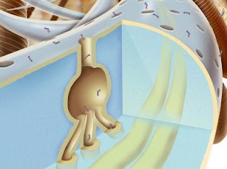
Caption: A special coating on the nanotunnels of a silk moth's antenna is the inspiration for a similar oily layer on synthetic nanopores, tiny measurement devices. University of Michigan researchers led the development of this improved technology, and they're using it to gain new insights into Alzheimer's and other similar neurodegenerative diseases.

Credit: Chris Burke. Usage Restrictions: None.

Silk Moth Closeup

Caption: This is a closeup of a nanotunnel in a silk moth's antenna. Pheromones travel through these tunnels, telling the male moth that a female is nearby.

Credit: Chris Burke. Usage Restrictions: None.

Nanopores

Caption: A new oily coating that improves the functionality of nanopores was inspired by a similar layer in the silk moth's antenna. Nanopores are measurement devices that enable the study of single molecules or proteins.

Credit: Chris Burke. Usage Restrictions: None.
"What this gives us is an improved tool to characterize biomolecules," Mayer said. "It allows us to gain understanding about their size, charge, shape, concentration and the speed at which they assemble. This could help us possibly diagnose and understand what is going wrong in a category of neurodegenerative disease that includes Parkinson's, Huntington's and Alzheimer's."

Mayer's "fluid lipid bilayer" resembles a coating on the male silk moth's antenna that helps it smell nearby female moths. The coating catches pheromone molecules in the air and carries them through nanotunnels in the exoskeleton to nerve cells that send a message to the bug's brain.

"These pheromones are lipophilic. They like to bind to lipids, or fat-like materials. So they get trapped and concentrated on the surface of this lipid layer in the silk moth. The layer greases the movement of the pheromones to the place where they need to be. Our new coating serves the same purpose," Mayer said.

One of Mayer's main research tracks is to study proteins called amyloid-beta peptides that are thought to coagulate into fibers that affect the brain in Alzheimer's. He is interested in studying the size and shape of these fibers and how they form.

"Existing techniques don't allow you to monitor the process very well. We wanted to see the clumping of these peptides using nanopores, but every time we tried it, the pores clogged up," Mayer said. "Then we made this coating, and now our idea works."

To use nanopores in experiments, researchers position the pore-pricked chip between two chambers of saltwater. They drop the molecules of interest into one of the chambers and send an electric current through the pore. As each molecule or protein passes through the pore, it changes the pore's electrical resistance. The amount of change observed tells the researchers valuable information about the molecule's size, electrical charge and shape.

Due to their small footprint and low power requirements, nanopores could also be used to detect biological warfare agents.

A research highlight on this work will appear in an upcoming edition of Nature. The paper is titled "Controlling protein translocation through nanopores with bio-inspired fluid walls."

###

This research is funded by the National Science Foundation, the National Institutes of Health, the Alzheimer's Disease Research Center, the Alzheimer's Association and the National Human Genome Research Institute. The university is pursuing patent protection for the intellectual property, and is seeking commercialization partners to help bring the technology to market.

For more information. Michael Mayer: biomembrane.engin.umich.edu/

Michigan Engineering:

The University of Michigan College of Engineering is ranked among the top engineering schools in the country. At $180 million annually, its engineering research budget is one of largest of any public university. Michigan Engineering is home to 11 academic departments, numerous research centers and expansive entrepreneurial programs. The College plays a leading role in the Michigan Memorial Phoenix Energy Institute and hosts the world-class Lurie Nanofabrication Facility. Michigan Engineering's premier scholarship, international scale and multidisciplinary scope combine to create The Michigan Difference. Find out more at www.engin.umich.edu/

Contact: Nicole Casal Moore ncmoore@umich.edu 734-647-7087 University of Michigan

Saturday, March 26, 2011

Berkeley Labs design material for hydrogen storage nanoparticles of magnesium metal sprinkled through matrix of polymethyl methacrylate

Since the 1970s, hydrogen has been touted as a promising alternative to fossil fuels due to its clean combustion —unlike hydrocarbon-based fuels, which spew greenhouse gases and harmful pollutants, hydrogen's only combustion by-product is water. Compared to gasoline, hydrogen is lightweight, can provide a higher energy density and is readily available. But there's a reason we're not already living in a hydrogen economy: to replace gasoline as a fuel, hydrogen must be safely and densely stored, yet easily accessed. Limited by materials unable to leap these conflicting hurdles, hydrogen storage technology has lagged behind other clean energy candidates.

In recent years, researchers have attempted to tackle both issues by locking hydrogen into solids, packing larger quantities into smaller volumes with low reactivity—a necessity in keeping this volatile gas stable. However, most of these solids can only absorb a small amount of hydrogen and require extreme heating or cooling to boost their overall energy efficiency.

Now, scientists with the U.S. Department of Energy (DOE) Lawrence Berkeley National Laboratory (Berkeley Lab) have designed a new composite material for hydrogen storage consisting of nanoparticles of magnesium metal sprinkled through a matrix of polymethyl methacrylate, a polymer related to Plexiglas. This pliable nanocomposite rapidly absorbs and releases hydrogen at modest temperatures without oxidizing the metal after cycling—a major breakthrough in materials design for hydrogen storage, batteries and fuel cells.

Nanocomposite for H Storage

Caption: This schematic shows high-capacity magnesium nanocrystals encapsulated in a gas-barrier polymer matrix to create a new and revolutionary hydrogen storage composite material.

Credit: Image from Jeff Urban. Usage Restrictions: None.

Jeff Urban and Team

Caption: From left, a scientific team that included Christian Kisielowski, Anne Ruminski, Rizia Bardhan and Jeff Urban has achieved a major breakthrough in the development nanocomposites for high-capacity hydrogen storage. Team members not shown are Ki-Joon Jeon and Hoi Ri Moon.

Credit: Photo by Roy Kaltschmidt, Berkeley Lab Public Affairs. Usage Restrictions: None.
"This work showcases our ability to design composite nanoscale materials that overcome fundamental thermodynamic and kinetic barriers to realize a materials combination that has been very elusive historically," says Jeff Urban, Deputy Director of the Inorganic Nanostructures Facility at the Molecular Foundry, a DOE Office of Science nanoscience center and national user facility located at Berkeley Lab. "Moreover, we are able to productively leverage the unique properties of both the polymer and nanoparticle in this new composite material, which may have broad applicability to related problems in other areas of energy research."

Urban, along with coauthors Ki-Joon Jeon and Christian Kisielowski used the TEAM 0.5 microscope at the National Center for Electron Microscopy (NCEM), another DOE Office of Science national user facility housed at Berkeley Lab, to observe individual magnesium nanocrystals dispersed throughout the polymer. With the high-resolution imaging capabilities of TEAM 0.5, the world's most powerful electron microscope, the researchers were also able to track defects—atomic vacancies in an otherwise-ordered crystalline framework—providing unprecedented insight into the behavior of hydrogen within this new class of storage materials.

"Discovering new materials that could help us find a more sustainable energy solution is at the core of the Department of Energy's mission. Our lab provides outstanding experiments to support this mission with great success," says Kisielowski. "We confirmed the presence of hydrogen in this material through time-dependent spectroscopic investigations with the TEAM 0.5 microscope. This investigation suggests that even direct imaging of hydrogen columns in such materials can be attempted using the TEAM microscope."

"The unique nature of Berkeley Lab encourages cross-division collaborations without any limitations," said Jeon, now at the Ulsan National Institute of Science and Technology, whose postdoctoral work with Urban led to this publication.

To investigate the uptake and release of hydrogen in their nanocomposite material, the team turned to Berkeley Lab's Energy and Environmental Technologies Division (EETD), whose research is aimed at developing more environmentally friendly technologies for generating and storing energy, including hydrogen storage.

"Here at EETD, we have been working closely with industry to maintain a hydrogen storage facility as well as develop hydrogen storage property testing protocols," says Samuel Mao, director of the Clean Energy Laboratory at Berkeley Lab and an adjunct engineering faculty member at the University of California (UC), Berkeley. "We very much enjoy this collaboration with Jeff and his team in the Materials Sciences Division, where they developed and synthesized this new material, and were then able to use our facility for their hydrogen storage research."

Adds Urban, "This ambitious science is uniquely well-positioned to be pursued within the strong collaborative ethos here at Berkeley Lab. The successes we achieve depend critically upon close ties between cutting-edge microscopy at NCEM, tools and expertise from EETD, and the characterization and materials know-how from MSD."

###

This research is reported in a paper titled, "Air-stable magnesium nanocomposites provide rapid and high-capacity hydrogen storage without heavy metal catalysts," appearing in the journal Nature Materials and available in Nature Materials online. Co-authoring the paper with Urban, Kisielowski and Jeon were Hoi Ri Moon, Anne M. Ruminski, Bin Jiang and Rizia Bardhan.

This work was supported by DOE's Office of Science.

The Molecular Foundry is one of the five DOE Nanoscale Science Research Centers (NSRCs), premier national user facilities for interdisciplinary research at the nanoscale. Together the NSRCs comprise a suite of complementary facilities that provide researchers with state-of-the-art capabilities to fabricate, process, characterize and model nanoscale materials, and constitute the largest infrastructure investment of the National Nanotechnology Initiative. The NSRCs are located at DOE's Argonne, Brookhaven, Lawrence Berkeley, Oak Ridge and Sandia and Los Alamos National Laboratories. For more information about the DOE NSRCs, please visit nano.energy.gov.

Lawrence Berkeley National Laboratory is a U.S. Department of Energy (DOE) national laboratory managed by the University of California for the DOE Office of Science. Berkeley Lab provides solutions to the world's most urgent scientific challenges including sustainable energy, climate change, human health, and a better understanding of matter and force in the universe. It is a world leader in improving our lives through team science, advanced computing, and innovative technology. Visit our Website at www.lbl.gov

Contact: Aditi Risbud asrisbud@lbl.gov 510-486-4861 DOE/Lawrence Berkeley National Laboratory

Nanoscale whiskers from tunicates, commonly known as sea squirts could grow human muscle tissue

Minute whiskers of nanoscale dimensions taken from sea creatures could hold the key to creating working human muscle tissue, University of Manchester researchers have discovered.

Scientists have found that cellulose from tunicates, commonly known as sea squirts, can influence the behaviour of skeletal muscle cells in the laboratory.

These nanostructures are several thousand times smaller than muscle cells and are the smallest physical feature found to cause cell alignment.

Alignment is important since a lot of tissue in the body, including muscle, contains aligned fibres which give it strength and stiffness.

Cellulose is a polysaccharide – a long chain of sugars joined together – usually found in plants and is the main component of paper and certain textiles such as cotton.

It is already being used for a number of different medical applications, including wound dressings, but this is the first time it has been proposed for creating skeletal muscle tissue.

sea squirtsTunicates grow on rocks and man-made structures in coastal waters around the world.

Cellulose extracted from tunicates is particularly well suited for making muscle tissue due to its unique properties.

University of Manchester academics Dr Stephen Eichhorn and Dr Julie Gough, working with PhD student James Dugan, chemically extract the cellulose in the form of nanowhiskers. One nanometre is one billionth of a metre and these minute whiskers are only 10s of nanometres wide – far thinner than a human hair.

When aligned and parallel to each other, they cause rapid muscle cell alignment and fusion.

The method is both simple and relatively quick, which could lead to doctors and scientists having the ability to create the normal aligned architecture of skeletal muscle tissue.

This tissue could be used to help repair existing muscle or even grow muscle from scratch.

Creating artificial tissue which can be used to replace damaged or diseased human muscles could revolutionise healthcare, and be of huge benefit to millions of people all over the world.

Dr Eichhorn thinks the cellulose extracted from the creatures could lead to a significant medical advancement. He added: “Although it is quite a detailed chemical process, the potential applications are very interesting.

“Cellulose is being looked at very closely around the world because of its unique properties, and because it is a renewable resource, but this is the first time that it has been used for skeletal muscle tissue engineering applications.

“There is potential for muscle precision engineering, but also for other architecturally aligned structures such as ligaments and nerves.”

PhD student James Dugan has become the first UK student to win the American Chemical Society’s Cellulose and Renewable Material Division award for his work on nanowhiskers.
Notes for editors

Dr Eichhorn, Dr Gough and Jim Dugan are available for interview on request.

The paper, Directing the Morphology and Differentiation of Skeletal Muscle Cells Using Oriented Cellulose Nanowhiskers, by James M. Dugan, Julie E Gough and Stephen J Eichhorn, is available on request from the Press Office.

University of Manchester For media enquiries please contact: Daniel Cochlin Media Relations Officer. The University of Manchester 0161 275 8387 daniel.cochlin@manchester.ac.uk

Thursday, March 24, 2011

New Measurement Into Biological Polymer Networks

ARLINGTON, Va. -- The development of a new measurement technology under a research project funded by the Air Force Office of Scientific Research and the National Science Foundation is probing the structure of composite and biological materials.

"Our results have provided some of the first microscopic insights into a sixty year old puzzle about the way polymeric networks react to repeated shear strains," said Dr. Daniel Blair, Assistant Professor, and principal investigator of the Soft Matter Group in the Department of Physics at Georgetown University.

Blair, Professor Andreas Bausch and other researchers at Technische Universtaet Muenchen (Technical University of Munich) used the muscle filament known as actin to construct a unique polymer network. In their quest to understand more about bio-polymers, they developed the rheometer and confocal microscope system (measures the mechanical properties of materials), which provide a unique and unprecedented level of precision and sensitivity for investigating polymeric systems which were previously too small to visualize during mechanical stress experiments. The rheometer and confocal microscopes clearly visualized the fluorescently labeled actin network and they filmed the polymer filaments'movement in 3-D when mechanical stress was applied.


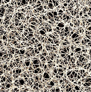
Confocal micrograph of an actin-filamin network

Confocal micrograph of an actin-filamin network. Credit: Kurt Schmoller, Technische Universtaet Muenchen (Technical University of Munich)
The rheometer and confocal microscopes, will help to lay the groundwork for future generations of materials that will possibly be used to create synthesized muscle tissue for the Air Force. These materials may even be ideally suited for powering micro-robots. The rheometer and confocal microscopes enabled the scientists to see the shearing process during the Mullins Effect when biological polymers become dramatically softer as seen in conventional polymers. Moreover, these materials also demonstrate dramatic strengthening in a way that is very different compared to conventional polymeric solids.

The researchers' next steps will be to use the Mullins Effect as a mechanical standard for understanding the properties of composite and biological networks.

"We will use confocal-rheology as a benchmark system for generating new collaborations and expanding the technique to other AFOSR sponsored projects," said Blair. "For example, in collaboration with Dr. Fritz Vollrath of the Oxford Silk Group and Dr. David Kaplan from Tufts University, we are investigating how shear stress influences the formation of silk fibers."

Blair noted that the new technology is impacting a number of other AFOSR supported projects as a platform for investigating the strengthening of nano-composite networks such as carbon nanotubes and cellulose nanofibers embedded in conventional materials.

Blair predicts that there will be possible private sector uses for the new technology in the area of the green revolution and its inherent smart, soft biological materials.

ABOUT AFOSR:
The Air Force Office of Scientific Research, located in Arlington, Virginia, continues to expand the horizon of scientific knowledge through its leadership and management of the Air Force's basic research program. As a vital component of the Air Force Research Laboratory, AFOSR's mission is to discover, shape, and champion basic science that profoundly impacts the future Air Force.

by Maria Callier Air Force Office of Scientific Research

Wednesday, March 23, 2011

Oxford Nanopore announces licence agreement with Harvard University for graphene DNA sequencing

Oxford, UK. Oxford Nanopore Technologies Ltd ("Oxford Nanopore") today announced an exclusive agreement with Harvard University's Office of Technology Development ("Harvard") for the development of graphene for DNA sequencing. Graphene is a robust, single atom thick 'honeycomb' lattice of carbon with high electrical conductivity. These properties make it an ideal material for high resolution, nanopore-based sequencing of single DNA molecules.

Under the terms of the agreement, Oxford Nanopore has exclusive rights to develop and commercialize methods for the use of graphene for the analysis of DNA and RNA, developed in the Harvard laboratories of Professors Jene Golovchenko, Daniel Branton, and Charles Lieber. The agreement adds to an existing collaboration between Oxford Nanopore and Harvard that spans basic methods of nanopore sensing through to the use of solid-state nanopores. Oxford Nanopore will also continue to support fundamental nanopore research at Harvard.

"Graphene is emerging as a wonder material for the 21st century and recent research has shown that it has transformative potential in DNA sequencing." said Dr Gordon Sanghera, CEO of Oxford Nanopore Technologies. "The groundbreaking research at Harvard lays the foundation for the development of a novel solid-state DNA sequencing device. We are proud to partner with the research team that pioneered early nanopore discoveries and continues to break boundaries with new materials and techniques.

Nanopore Created in Graphene with DNA

Caption: A nanopore is created in graphene to form a trans-electrode, measuring variations in current as a single DNA molecule passes through the pore.

Credit: iemedia solutions/ONT. Usage Restrictions: None.
"Oxford Nanopore is probably best known for protein nanopores," continued Dr Sanghera. "However, today's agreement highlights that we are increasing our investment in solid-state nanopores by adding graphene to our existing portfolio of solid-state nanopore projects and collaborations."

In a landmark 2010 Nature publication (S. Garaj et al, Nature Vol 467,doi:10.1038/nature09379) the Harvard team and collaborators used graphene to separate two chambers containing ionic solutions, and created a hole - a nanopore – in the graphene. The group demonstrated that the graphene nanopore could be used as a trans-electrode, measuring a current flowing through the nanopore between two chambers. The trans-electrode was used to measure variations in the current as a single molecule of DNA was passed through the nanopore. This resulted in a characteristic electrical signal that reflected the size and conformation of the DNA molecule.

At one atom thick, graphene is believed to be the thinnest membrane able to separate two liquid compartments from each other. This is an important characteristic for DNA sequencing; a trans-electrode of this thickness would be suitable for the accurate analysis of individual bases on a DNA polymer as it passes through the graphene.

Nanopore techniques aim to improve substantially the cost, power and complexity of DNA sequencing. While first generation technologies in development at Oxford Nanopore use nanopores made by porous proteins, subsequent generations will use synthetic 'solid-state' materials such as silicon nitride. However, at this time challenges remain in industrial fabrication of synthetic nanopores with the required dimensions and electronic properties. Graphene offers a potential solution due to its strength, dimensions, electrical properties and future potential for low-cost manufacturing.

###

Oxford Nanopore Technologies

Oxford Nanopore Technologies Ltd is developing a novel technology for direct, electronic detection and analysis of single molecules using nanopores. The GridION technology platform (x.co/Trk2) is designed to offer substantial benefits in a variety of applications; the Company's lead application is DNA sequencing but the platform is adaptable for the analysis of proteins and other single molecules.

DNA sequencing techniques in development include exonuclease sequencing and strand sequencing, both of which combine a protein nanopore with a processive enzyme, multiplexed on a silicon chip. The Company also has collaborations for the development of solid-state nanopores.

Oxford Nanopore has collaborations and exclusive licensing deals with leading institutions including the University of Oxford, Harvard and UCSC. The Company has funding programmes in these laboratories to support the science of nanopore sensing. Oxford Nanopore has licensed or owns more than 250 patents and patent applications that relate to all aspects of nanopore sensing from protein nanopores to solid state nanopores and for the analysis of DNA, proteins and other molecules. This includes the use of functionalised solid-state nanopores for molecular characterisation, methods of fabricating solid-state nanopores and modifications of solid-state nanopores to adjust sensitivity or other parameters. For more information about the Company's patent x.co/Trk1

For further information about the company please visit www.nanoporetech.com.

Notes to Editors Nature publication 1Graphene as a subnanometre trans-electrode membrane, S. Garaj, W. Hubbard, A. Reina, J. Kong, D. Branton & J. A. Golovchenko. Nature Vol 467,doi:10.1038/nature09379 (Sept 2010) www.nature.com/nature/journal/v467/n7312/abs/nature09

This publication describes the use of graphene as a trans-electrode, detecting a DNA strand as it passes through a hole in the graphene sheet.

A sheet of graphene was stretched over a silicon-based frame, and inserted between two separate liquid reservoirs. An electrical voltage was applied between the reservoirs and when a nanopore was formed in the graphene this allowed the flow of an ionic current through the nanopore. This current could be measured as an electrical current signal using the trans-electrode properties of graphene.

Double-stranded DNA strands were added to one chamber and electrophoretically driven through the nanopore. This created a characteristic electrical signal that reflected the size and conformation of the DNA molecule. Graphene is thin enough to interact with individual nucleotides on a DNA strand as it passes through the nanopore, and therefore suitable for further development as a solid state DNA sequencing tool.

Graphene

Graphene is a single atom thick sheet of carbon – one layer of graphite. The carbon atoms are arranged in a hexagonal planar structure. Graphene has extremely high strength-to-weight ratio and has higher electrical conductivity than silicon. The material has been proposed as suitable for many future applications including a range of electronic nanodevices, batteries, touch screens, transmitters and receivers for broadband communications.

In 2010, the Nobel Prize for Physics was awarded to two scientists who made and discovered the properties of graphene, Professors Andre Geim and Konstantin Novoselov of the University of Manchester, UK. Institute of Physics briefing on graphene: www.iop.org/publications/iop/2011/

Tuesday, March 22, 2011

ultra-low-power digital memory that is faster and uses 100 times less energy than similar available memory

New technology would dramatically extend battery life for mobile devices.

CHAMPAIGN, Ill. — Technophiles who have been dreaming of mobile devices that run longer on lighter, slimmer batteries may soon find their wish has been granted.

University of Illinois engineers have developed a form of ultra-low-power digital memory that is faster and uses 100 times less energy than similar available memory. The technology could give future portable devices much longer battery life between charges.

Led by electrical and computer engineering professor Eric Pop, the team will publish its results in an upcoming issue of Science magazine and online in the March 10 Science Express.

"I think anyone who is dealing with a lot of chargers and plugging things in every night can relate to wanting a cell phone or laptop whose batteries can last for weeks or months," said Pop, who is also affiliated with the Beckman Institute for Advanced Science and Technology at Illinois.

The flash memory used in mobile devices today stores bits as charge, which requires high programming voltages and is relatively slow. Industry has been exploring faster, but higher power phase-change materials (PCM) as an alternative. In PCM memory a bit is stored in the resistance of the material, which is switchable.

Eric Pop Research Group

Caption: A team of electrical engineers, led by Illinois professor Eric Pop, developed ultra-low-power memory that uses 100 times less energy than existing state-of-the-art memory. Back row, L-R: Professor Eric Pop, David Estrada, Albert Liao. Front: Feng Xiong.

Credit: L. Brian Stauffer. Usage Restrictions: None.

PCM Carbon Nanotube Bits

Caption: This is a schematic of four bits in various on/off states. The bit is made up of phase-change material with a size of about 10 nanometers with carbon nanotube electrodes. The programming current is 100 times lower than the present state-of-the-art memory.

Credit: Eric Pop, University of Illinois. Usage Restrictions: None.
Pop's group lowered the power per bit to 100 times less than existing PCM memory by focusing on one simple, yet key factor: size.

Rather than the metal wires standard in industry, the group used carbon nanotubes, tiny tubes only a few nanometers in diameter – 10,000 times smaller than a human hair.

"The energy consumption is essentially scaled with the volume of the memory bit," said graduate student Feng Xiong, the first author of the paper. "By using nanoscale contacts, we are able to achieve much smaller power consumption."

To create a bit, the researchers place a small amount of PCM in a nanoscale gap formed in the middle of a carbon nanotube. They can switch the bit "on" and "off" by passing small currents through the nanotube.

"Carbon nanotubes are the smallest known electronic conductors," Pop said. "They are better than any metal at delivering a little jolt of electricity to zap the PCM bit."

Nanotubes also boast an extraordinary stability, as they are not susceptible to the degradation that can plague metal wires. In addition, the PCM that functions as the actual bit is immune to accidental erasure from a passing scanner or magnet.

The low-power PCM bits could be used in existing devices with a significant increase in battery life. Right now, a smart phone uses about a watt of energy and a laptop runs on more than 25 watts. Some of that energy goes to the display, but an increasing percentage is dedicated to memory.

"Anytime you're running an app, or storing MP3s, or streaming videos, it's draining the battery," said Albert Liao, a graduate student and co-author.
"The memory and the processor are working hard retrieving data. As people use their phones to place calls less and use them for computing more, improving the data storage and retrieval operations is important."

Pop believes that, along with improvements in display technology, the nanotube PCM memory could increase an iPhone's energy efficiency so it could run for a longer time on a smaller battery, or even to the point where it could run simply by harvesting its own thermal, mechanical or solar energy – no battery required.

And device junkies will not be the only beneficiaries.

"We're not just talking about lightening our pockets or purses," Pop said. "This is also important for anything that has to operate on a battery, such as satellites, telecommunications equipment in remote locations, or any number of scientific and military applications."

In addition, ultra-low-power memory could cut the energy consumption – and thus the expense – of data storage or supercomputing centers by a large percentage. The low-power memory could also enable three-dimensional integration, a stacking of chips that has eluded researchers because of fabrication and heat problems.

The team has made and tested a few hundred bits so far, and they want to scale up production to create arrays of memory bits that operate together. They also hope to achieve greater data density through clever programming such that each physical PCM bit can program two data bits, called multibit memory.

The team is continuing to work to reduce power consumption and increase energy efficiency even beyond the groundbreaking savings they've already demonstrated.

"Even though we've taken one technology and shown that it can be improved by a factor of 100, we have not yet reached what is physically possible. We have not even tested the limits yet. I think we could lower power by at least another factor of 10," Pop said.

###

The work was supported in part by the Marco Focus Center Research Program, a Semiconductor Research Corporation entity, and by the Office of Naval Research. Graduate student David Estrada was also a co-author.

Editor's note: To reach Eric Pop, call 217-244-2070; epop@illinois.edu.

Contact: Liz Ahlberg eahlberg@illinois.edu 217-244-1073 University of Illinois at Urbana-Champaign

Monday, March 21, 2011

A new "templated growth" technique for fabricating nanoribbons of epitaxial graphene

Technique Produces Graphene Nanoribbons with Metallic Properties.

A new "templated growth" technique for fabricating nanoribbons of epitaxial graphene has produced structures just 15 to 40 nanometers wide that conduct current with almost no resistance. These structures could address the challenge of connecting graphene devices made with conventional architectures -- and set the stage for a new generation of devices that take advantage of the quantum properties of electrons.

"We can now make very narrow, conductive nanoribbons that have quantum ballistic properties," said Walt de Heer, a professor in the School of Physics at the Georgia Institute of Technology. "These narrow ribbons become almost like a perfect metal. Electrons can move through them without scattering, just like they do in carbon nanotubes."

De Heer discussed recent results of this graphene growth process March 21st at the American Physical Society’s March 2011 Meeting in Dallas. The research was sponsored by the National Science Foundation-supported Materials Research Science and Engineering Center (MRSEC).

First reported Oct. 3 in the advance online edition of the journal Nature Nanotechnology, the new fabrication technique allows production of epitaxial graphene structures with smooth edges. Earlier fabrication techniques that used electron beams to cut graphene sheets produced nanoribbon structures with rough edges that scattered electrons, causing interference. The resulting nanoribbons had properties more like insulators than conductors.

Walt de Heer

A team of Georgia Tech researchers led by Professor Walt de Heer has pioneered techniques for fabricating epitaxial graphene nanoribbons using a templated growth technique. The equipment shown behind de Heer is used to characterize graphene properties.
"In our templated growth approach, we have essentially eliminated the edges that take away from the desirable properties of graphene," de Heer explained. "The edges of the epitaxial graphene merge into the silicon carbide, producing properties that are really quite interesting."

The templated growth technique begins with etching patterns into the silicon carbide surfaces on which epitaxial graphene is grown. The patterns serve as templates directing the growth of graphene structures, allowing the formation of nanoribbons and other structures of specific widths and shapes without the use of cutting techniques that produce the rough edges.

In creating these graphene nanostructures, de Heer and his research team first use conventional microelectronics techniques to etch tiny "steps" -- or contours -- into a silicon carbide wafer whose surface has been made extremely flat. They then heat the contoured wafer to approximately 1,500 degrees Celsius, which initiates melting that polishes any rough edges left by the etching process.

Established techniques are then used for growing graphene from silicon carbide by driving the silicon atoms from the surface. Instead of producing a consistent layer of graphene across the entire surface of the wafer, however, the researchers limit the heating time so that graphene grows only on portions of the contours.

The width of the resulting nanoribbons is proportional to the depth of the contours, providing a mechanism for precisely controlling the nanoribbon structures. To form complex structures, multiple etching steps can be carried out to create complex templates.

"This technique allows us to avoid the complicated e-beam lithography steps that people have been using to create structures in epitaxial graphene," de Heer noted. "We are seeing very good properties that show these structures can be used for real electronic applications."

Since publication of the Nature Nanotechnology paper, de Heer's team has been refining its technique. "We have taken this to an extreme -- the cleanest and narrowest ribbons we can make," he said. "We expect to be able to do everything we need with the size ribbons that we are able to make right now, though we probably could reduce the width to 10 nanometers or less."

While the Georgia Tech team is continuing to develop high-frequency transistors -- perhaps even at the terahertz range -- its primary effort now focuses on developing quantum devices, de Heer said. Such devices were envisioned in the patents Georgia Tech holds on various epitaxial graphene processes.

"This means that the way we will be doing graphene electronics will be different," he explained. "We will not be following the model of using standard field-effect transistors (FETs), but will pursue devices that use ballistic conductors and quantum interference. We are headed straight into using the electron wave effects in graphene."

Taking advantage of the wave properties will allow electrons to be manipulated with techniques similar to those used by optical engineers. For instance, switching may be carried out using interference effects -- separating beams of electrons and then recombining them in opposite phases to extinguish the signals.

Quantum devices would be smaller than conventional transistors and operate at lower power. Because of its ability to transport electrons with virtually no resistance, epitaxial graphene may be the ideal material for such devices, de Heer said.

"Using the quantum properties of electrons rather than the standard charged-particle properties means opening up new ways of looking at electronics," he predicted. "This is probably the way that electronics will evolve, and it appears that graphene is the ideal material for making this transition."

De Heer's research team hopes to demonstrate a rudimentary switch operating on the quantum interference principle within a year.

Epitaxial graphene may be the basis for a new generation of high-performance devices that will take advantage of the material's unique properties in applications where higher costs can be justified. Silicon, today's electronic material of choice, will continue to be used in applications where high-performance is not required, de Heer said.

"This is an important step in the process," he added. "There are going to be a lot of surprises as we move into these quantum devices and find out how they work. We have good reason to believe that this can be the basis for a new generation of transistors based on quantum interference."

Research News & Publications Office, Georgia Institute of Technology. 75 Fifth Street, N.W., Suite 314, Atlanta, Georgia 30308 USA. Media Relations Contacts: John Toon Research News & Publications Office (404-894-6986) (jtoon@gatech.edu) or Abby Robinson (404-385-3364) (abby@innovate.gatech.edu). Writer: John Toon.

Sunday, March 20, 2011

Rice University lab uses ruthenium complexes to dissolve nanotubes, add functionality

A lab at Rice University has stepped forward with an efficient method to disperse nanotubes in a way that preserves their unique properties -- and adds more.

The new technique allows inorganic metal complexes with different functionalities to remain in close contact with single-walled carbon nanotubes while keeping them separated in a solution.

That separation is critical to manufacturers who want to spin fiber from nanotubes, or mix them into composite materials for strength or to take advantage of their electrical properties. For starters, the ability to functionalize the nanotubes at the same time may advance imaging sensors, catalysis and solar-activated hydrogen fuel cells.

Better yet, a batch of nanotubes can apparently stay dispersed in water for weeks on end.

Keeping carbon nanotubes from clumping in aqueous solutions and combining them with molecules that add novel abilities have been flies in the ointment for scientists exploring the use of these highly versatile materials.

Avishek Saha, Professor Angel Marti and Disha Jain

CAPTION: Rice researchers -- from left, Avishek Saha, Professor Angel Marti and Disha Jain -- found an efficient way to both dissolve and functionalize carbon nanotubes in a solution. (Credit: Rice University)
They've tried attaching organic molecules to the nanotubes' surfaces to add functionality as well as solubility. But while these techniques can separate nanotubes from one another, they take a toll on the nanotubes' electronic, thermal and mechanical properties.

Angel Marti, a Rice assistant professor of chemistry and bioengineering and a Norman Hackerman-Welch Young Investigator, and his students reported this month in the Royal Society of Chemistry journal Chemical Communications that ruthenium polypyridyl complexes are highly effective at dispersing nanotubes in water efficiently and for long periods. Ruthenium is a rare metallic element.

One key is having just the right molecule for the job. Marti and his team created ruthenium complexes by combining the element with ligands, stable molecules that bind to metal ions. The resulting molecular complex is part hydrophobic (the ligands) and part hydrophilic (the ruthenium). The ligands strongly bind to nanotubes while the attached ruthenium molecules interact with water to maintain the tubes in solution and keep them apart from one another.

Another key turned out to be moderation.

Originally, Marti said, he and co-authors Disha Jain and Avishek Saha weren't out to solve a problem that has boggled chemists for decades, but their willingness to "do something crazy" paid off big-time. Jain is a former postdoctoral researcher in Marti’s lab, and Saha is a graduate student.

The researchers were eyeing ruthenium complexes as part of a study to track amyloid deposits associated with Alzheimer's disease. "We started to wonder what would happen if we modified the metal complex so it could bind to a nanotube," Marti said. "That would provide solubility, individualization, dispersion and functionality."

It did, but not at first. "Avishek put this together with purified single-walled carbon nanotubes (created via Rice's HiPco process) and sonicated. Absolutely nothing happened. The nanotubes didn't get into solution -- they just clumped at the bottom.

"That was very weird, but that's how science works -- some things you think are good ideas never work."

Saha removed the liquid and left the clumped nanotubes at the bottom of the centrifuge tube. "So I said, 'Well, why don't you do something crazy. Just add water to that, and with the little bit of ruthenium that might remain there, try to do the reaction.' He did that, and the solution turned black."

A low concentration of ruthenium did the trick. "We found out that 0.05 percent of the ruthenium complex is the optimum concentration to dissolve nanotubes," Marti said. Further experimentation showed that simple ruthenium complexes alone did not work. The molecule requires its hydrophobic ligand tail, which seeks to minimize its exposure to water by binding with nanotubes. "That's the same thing nanotubes want to do, so it's a favorable relationship," he said.

Marti also found the nanotubes' natural fluorescence unaffected by the ruthenium complexes. "Even though they've been purified, which can introduce defects, they still exhibit very good fluorescence," he said.

He said that certain ruthenium complexes have the ability to stay in an excited state for a long time -- about 600 nanoseconds, or 100 times longer than normal organic molecules. "It means the probability that it will transfer an electron is high. That's convenient for energy transfer applications, which are important for imaging," he said.

That nanotubes stay suspended for a long time should catch the eye of manufacturers who use them in bulk. "They should stay separated for weeks without problems," Marti said. "We have solutions that have been sitting for months without any signs of crashing."

The Welch Foundation supported the research.

Contact: David Ruth druth@rice.edu 713-348-6327 Rice University

Friday, March 18, 2011

A new way to think about the structure of space

Is space like a chessboard? Physicists at UCLA set out to design a better transistor and ended up discovering a new way to think about the structure of space.

Space is usually considered infinitely divisible — given any two positions, there is always a position halfway between. But in a recent study aimed at developing ultra-fast transistors using graphene, researchers from the UCLA Department of Physics and Astronomy and the California NanoSystems Institute show that dividing space into discrete locations, like a chessboard, may explain how point-like electrons, which have no finite radius, manage to carry their intrinsic angular momentum, or "spin."

While studying graphene's electronic properties, professor Chris Regan and graduate student Matthew Mecklenburg found that a particle can acquire spin by living in a space with two types of positions — dark tiles and light tiles. The particle seems to spin if the tiles are so close together that their separation cannot be detected.

"An electron's spin might arise because space at very small distances is not smooth, but rather segmented, like a chessboard," Regan said.

Their findings are published in the March 18 edition of the journal Physical Review Letters.

Electron Spin and Graphene

Electrons are thought to spin, even though they are pure point particles with no surface that can possibly rotate. Recent work on graphene shows that the electron’s spin might arise because space at very small distances is not smooth, but rather segmented like a chessboard.

The standard cartoon of an electron shows a spinning sphere with positive or negative angular momentum, as illustrated in blue or gold above. However, such cartoons are fundamentally misleading: compelling experimental evidence indicates that electrons are ideal point particles, with no finite radius or internal structure that could possibly “spin”.

A quantum mechanical model of electron transport in graphene, a single layer of graphite (shown as a black honeycomb), presents a possible resolution to this puzzle. An electron in graphene hops from carbon atom to carbon atom as if moving on a chessboard with triangular tiles. At low energies the individual tiles are unresolved, but the electron acquires an “internal” spin quantum number which reflects whether it is on the blue or the gold tiles. Thus the electron’s spin could arise not from rotational motion of its substructure, but rather from the discrete, chessboard-like structure of space.

(Image: Chris Regan/CNSI)
In quantum mechanics, "spin up" and "spin down" refer to the two types of states that can be assigned to an electron. That the electron's spin can have only two values — not one, three or an infinite number — helps explain the stability of matter, the nature of the chemical bond and many other fundamental phenomena.

However, it is not clear how the electron manages the rotational motion implied by its spin. If the electron had a radius, the implied surface would have to be moving faster than the speed of light, violating the theory of relativity. And experiments show that the electron does not have a radius; it is thought to be a pure point particle with no surface or substructure that could possibly spin.

In 1928, British physicist Paul Dirac showed that the spin of the electron is intimately related to the structure of space-time. His elegant argument combined quantum mechanics with special relativity, Einstein's theory of space-time (famously represented by the equation E=mc2).

Dirac's equation, far from merely accommodating spin, actually demands it. But while showing that relativistic quantum mechanics requires spin, the equation does not give a mechanical picture explaining how a point particle manages to carry angular momentum, nor why this spin is two-valued.

Unveiling a concept that is at once novel and deceptively simple, Regan and Mecklenburg found that electrons' two-valued spin can arise from having two types of tiles — light and dark — in a chessboard-like space. And they developed this quantum mechanical model while working on the surprisingly practical problem of how to make better transistors out of a new material called graphene.

Graphene, a single sheet of graphite, is an atomically-thin layer of carbon atoms arranged in a honeycomb structure. First isolated in 2004 by Andre Geim and Kostya Novoselov, graphene has a wealth of extraordinary electronic properties, such as high electron mobility and current capacity. In fact, these properties hold such promise for revolutionary advances that Geim and Novoselov were awarded the 2010 Nobel Prize a mere six years after their achievement.

Regan and Mecklenburg are part of a UCLA effort to develop extremely fast transistors using this new material.

"We wanted to calculate the amplification of a graphene transistor," Mecklenburg said. "Our collaboration was building them and needed to know how well they were going to work."

This calculation involved understanding how light interacts with the electrons in graphene.

The electrons in graphene move by hopping from carbon atom to carbon atom, as if hopping on a chessboard. The graphene chessboard tiles are triangular, with the dark tiles pointing "up" and light ones pointing "down." When an electron in graphene absorbs a photon, it hops from light tiles to dark ones. Mecklenburg and Regan showed that this transition is equivalent to flipping a spin from "up" to "down."

In other words, confining the electrons in graphene to specific, discrete positions in space gives them spin. This spin, which derives from the special geometry of graphene's honeycomb lattice, is in addition to and distinct from the usual spin carried by the electron. In graphene the additional spin reflects the unresolved chessboard-like structure to the space that the electron occupies.

"My adviser [Regan] spent his Ph.D. studying the structure of the electron," Mecklenburg said. "So he was very excited to see that spin can emerge from a lattice. It makes you wonder if the usual electron spin could be generated in the same way."

"It's not yet clear if this work will be more useful in particle or condensed matter physics," Regan said, "but it would be odd if graphene's honeycomb structure was the only lattice capable of generating spin."

The California NanoSystems Institute at UCLA is an integrated research facility located at UCLA and UC Santa Barbara. Its mission is to foster interdisciplinary collaborations in nanoscience and nanotechnology; to train a new generation of scientists, educators and technology leaders; to generate partnerships with industry; and to contribute to the economic development and the social well-being of California, the United States and the world. The CNSI was established in 2000 with $100 million from the state of California.

An additional $850 million of support has come from federal research grants and industry funding. CNSI members are drawn from UCLA's College of Letters and Science, the David Geffen School of Medicine, the School of Dentistry, the School of Public Health and the Henry Samueli School of Engineering and Applied Science. They are engaged in measuring, modifying and manipulating atoms and molecules — the building blocks of our world. Their work is carried out in an integrated laboratory environment. This dynamic research setting has enhanced understanding of phenomena at the nanoscale and promises to produce important discoveries in health, energy, the environment and information technology.

Media Contacts: Jennifer Marcus, 310-267-4839 jmarcus@cnsi.ucla.edu

Thursday, March 17, 2011

Two atoms in separate locations to take turns jiggling back and forth while swapping the smallest measurable units of energy

Quantum hot potato: NIST researchers entice 2 atoms to swap smallest energy units, New technique has potential to simplify future information processing.

BOULDER, Colo.—Physicists at the National Institute of Standards and Technology (NIST) have for the first time coaxed two atoms in separate locations to take turns jiggling back and forth while swapping the smallest measurable units of energy. By directly linking the motions of two physically separated atoms, the technique has the potential to simplify information processing in future quantum computers and simulations.

Described in a paper published Feb. 23 by Nature,* the NIST experiments enticed two beryllium ions (electrically charged atoms) to take turns vibrating in an electromagnetic trap, exchanging units of energy, or quanta, that are a hallmark of quantum mechanics. As little as one quantum was traded back and forth in these exchanges, signifying that the ions are "coupled" or linked together. These ions also behave like objects in the larger, everyday world in that they are "harmonic oscillators" similar to pendulums and tuning forks, making repetitive, back-and-forth motions.

NIST Ion Trap

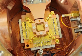
Caption: NIST physicists used this apparatus to coax two beryllium ions (electrically charged atoms) into swapping the smallest measurable units of energy back and forth, a technique that may simplify information processing in a quantum computer. The ions are trapped about 40 micrometers apart above the square gold chip in the center. The chip is surrounded by a copper enclosure and gold wire mesh to prevent buildup of static charge.

Credit: Y. Colombe / NIST. Usage Restrictions: Please use proper credit.
"First one ion is jiggling a little and the other is not moving at all; then the jiggling motion switches to the other ion. The smallest amount of energy you could possibly see is moving between the ions," explains first author Kenton Brown, a NIST post-doctoral researcher. "We can also tune the coupling, which affects how fast they exchange energy and to what degree. We can turn the interaction on and off."

The experiments were made possible by a novel, one-layer ion trap cooled to minus 269 C (minus 452 F) with a liquid helium bath. The ions, 40 micrometers apart, float above the surface of the trap. In contrast to a conventional two-layer trap, the surface trap features smaller electrodes and can position ions closer together, enabling stronger coupling. Chilling to cryogenic temperatures suppresses unwanted heat that can distort ion behavior.

The energy swapping demonstrations begin by cooling both ions with a laser to slow their motion. Then one ion is cooled further to a motionless state with two opposing ultraviolet laser beams. Next the coupling interaction is turned on by tuning the voltages of the trap electrodes. In separate experiments reported in Nature, NIST researchers measured the ions swapping energy at levels of several quanta every 155 microseconds and at the single quantum level somewhat less frequently, every 218 microseconds. Theoretically, the ions could swap energy indefinitely until the process is disrupted by heating. NIST scientists observed two round-trip exchanges at the single quantum level.

To detect and measure the ions' activity, NIST scientists apply an oscillating pulse to the trap at different frequencies while illuminating both ions with an ultraviolet laser and analyzing the scattered light. Each ion has its own characteristic vibration frequency; when excited, the motion reduces the amount of laser light absorbed. Dimming of the scattered light tells scientists an ion is vibrating at a particular pulse frequency.

To turn on the coupling interaction, scientists use electrode voltages to tune the frequencies of the two ions, nudging them closer together. The coupling is strongest when the frequencies are closest. The motions become linked due to the electrostatic interactions of the positively charged ions, which tend to repel each other. Coupling associates each ion with both characteristic frequencies.

The new experiments are similar to the same NIST research group's 2009 demonstration of entanglement—a quantum phenomenon linking properties of separated particles—in a mechanical system of two separated pairs of vibrating ions. However, the new experiments coupled the oscillators' motions more directly than before and, therefore, may simplify information processing. In this case the researchers observed quantum behavior but did not verify entanglement.

The new technique could be useful in a future quantum computer, which would use quantum systems such as ions to solve problems that are intractable today. For example, quantum computers could break today's most widely used data encryption codes. Direct coupling of ions in separate locations could simplify logic operations and help correct processing errors. The technique is also a feature of proposals for quantum simulations, which may help explain the mechanisms of complex quantum systems such as high-temperature superconductors.

In addition, the demonstration also suggests that similar interactions could be used to connect different types of quantum systems, such as a trapped ion and a particle of light (photon), to transfer information in a future quantum network. For example, a trapped ion could act as a "quantum transformer" between a superconducting quantum bit (qubit) and a qubit made of photons.

###

As a non-regulatory agency, NIST promotes U.S. innovation and industrial competitiveness by advancing measurement science, standards and technology in ways that enhance economic security and improve our quality of life.

* K.R. Brown, C. Ospelkaus, Y. Colombe, A.C. Wilson, D. Leibfried & D.J. Wineland. 2010. Coupled quantized mechanical oscillators. Nature. Published online Feb. 23.

Contact: Laura Ost laura.ost@nist.gov || National Institute of Standards and Technology (NIST)

Wednesday, March 16, 2011

MIT engineers have designed a new type of nanoparticle that could safely and effectively deliver vaccines for diseases such as HIV and malaria

Nano-sized vaccines, New MIT nanoparticles could lead to powerful vaccines for HIV and other diseases.

CAMBRIDGE, Mass.- MIT engineers have designed a new type of nanoparticle that could safely and effectively deliver vaccines for diseases such as HIV and malaria.

The new particles, described in the Feb. 20 issue of Nature Materials, consist of concentric fatty spheres that can carry synthetic versions of proteins normally produced by viruses. These synthetic particles elicit a strong immune response — comparable to that produced by live virus vaccines — but should be much safer, says Darrell Irvine, author of the paper and an associate professor of materials science and engineering and biological engineering.

Such particles could help scientists develop vaccines against cancer as well as infectious diseases. In collaboration with scientists at the Walter Reed Army Institute of Research, Irvine and his students are now testing the nanoparticles' ability to deliver an experimental malaria vaccine in mice.

Vaccines protect the body by exposing it to an infectious agent that primes the immune system to respond quickly when it encounters the pathogen again. In many cases, such as with the polio and smallpox vaccines, a dead or disabled form of the virus is used. Other vaccines, such as the diphtheria vaccine, consist of a synthetic version of a protein or other molecule normally made by the pathogen.

Immune cells, tagged with green fluorescent protein

Immune cells, tagged with green fluorescent protein, are surrounded by nanoparticles (red), after the nanoparticles are injected into the skin of a mouse. Photo: Peter DeMuth and James Moon
When designing a vaccine, scientists try to provoke at least one of the human body's two major players in the immune response: T cells, which attack body cells that have been infected with a pathogen; or B cells, which secrete antibodies that target viruses or bacteria present in the blood and other body fluids.

For diseases in which the pathogen tends to stay inside cells, such as HIV, a strong response from a type of T cell known as "killer" T cell is required. The best way to provoke these cells into action is to use a killed or disabled virus, but that cannot be done with HIV because it's difficult to render the virus harmless.

To get around the danger of using live viruses, scientists are working on synthetic vaccines for HIV and other viral infections such as hepatitis B. However, these vaccines, while safer, do not elicit a very strong T cell response. Recently, scientists have tried encasing the vaccines in fatty droplets called liposomes, which could help promote T cell responses by packaging the protein in a virus-like particle. However, these liposomes have poor stability in blood and body fluids.

Irvine, who is a member of MIT's David H. Koch Institute for Integrative Cancer Research, decided to build on the liposome approach by packaging many of the droplets together in concentric spheres. Once the liposomes are fused together, adjacent liposome walls are chemically "stapled" to each other, making the structure more stable and less likely to break down too quickly following injection. However, once the nanoparticles are absorbed by a cell, they degrade quickly, releasing the vaccine and provoking a T cell response.

In tests with mice, Irvine and his colleagues used the nanoparticles to deliver a protein called ovalbumin, an egg-white protein commonly used in immunology studies because biochemical tools are available to track the immune response to this molecule. They found that three immunizations of low doses of the vaccine produced a strong T cell response — after immunization, up to 30 percent of all killer T cells in the mice were specific to the vaccine protein.

That is one of the strongest T cell responses generated by a protein vaccine, and comparable to strong viral vaccines, but without the safety concerns of live viruses, says Irvine. Importantly, the particles also elicit a strong antibody response.

In addition to the malaria studies with scientists at Walter Reed, Irvine is also working on developing the nanoparticles to deliver cancer vaccines and HIV vaccines. Translation of this approach to HIV is being done in collaboration with colleagues at the Ragon Institute of MIT, Harvard and Massachusetts General Hospital. The institute, which funded this study along with the Gates Foundation, Department of Defense and National Institutes of Health, was established in 2009 with the goal of developing an HIV vaccine.

###

Written by Anne Trafton, MIT News Office Contact: Caroline McCall cmccall5@mit.edu 617-253-1682 Massachusetts Institute of Technology

Nanoparticles to improve survival after life-threatening blood loss

(BRONX, NY) — In an advance that could improve battlefield and trauma care, scientists at Albert Einstein College of Medicine of Yeshiva University have used tiny particles called nanoparticles to improve survival after life-threatening blood loss. Nanoparticles containing nitric oxide (NO) were infused into the bloodstream of hamsters, where they helped maintain blood circulation and protect vital organs. The research was reported in the February 21 online edition of the journal Resuscitation.

"The new nanomedicine was developed to address the need for better field treatments for massive human blood loss, which can cause cardiovascular collapse, also known as hemorrhagic shock. This potentially fatal condition is best treated with infusions of refrigerated blood and other fluids. But such treatments are limited to emergency rooms or trauma centers.

"It is highly impractical to pack these supplies for use in rural emergencies, mass-casualty disasters or on the battlefield," said coauthor Joel Friedman, M.D., Ph.D., professor of physiology & medicine and of medicine and the Young Men's Division Chair in Physiology at Einstein. "Our nanoparticle therapy may offer the potential for saving lives in those situations. It's lightweight and compact and doesn't require refrigeration."

Joel Friedman, M.D., Ph.D.The new therapy counters hemorrhagic shock by increasing the body's levels of NO gas, which, among other physiological functions, relaxes blood vessels and regulates blood pressure. The gas was encased in microscopic-sized particles that were specially designed by the Einstein team. (NO is so short-lived that delivering it in therapeutic amounts requires a method of sustained release.) The therapy is created by adding the NO-containing nanoparticles to saline solution, which was then infused into the animals. Once in the body, the nanoparticles gradually release a sustained dose of NO to tissues.

The nanomedicine was successfully tested in hamsters that had lost half their blood volume. "Animals given the nanoparticles exhibited better cardiac stability, stronger blood flow to tissues and other measures of hemorrhagic shock recovery compared to controls receiving saline solution minus the nanoparticles," reported Dr. Friedman.

Previously published studies by Dr. Friedman and colleagues have demonstrated the beneficial effects of NO-containing nanoparticles for healing antibiotic-resistant staph infections and abscess caused by those bacteria and for treating erectile dysfunction.

The paper, "Exogenous Nitric Oxide Prevents Cardiovascular Collapse During Hemorrhagic Shock," appears in the Februrary 21, 2011 online edition of Resuscitation. Other Einstein authors of the study were Adam Friedman, M.D. and Parimala Nachuraju, Ph.D. Coauthor Pedro Cabrales, Ph.D., of the department of bioengineering at the University of California, San Diego, California, carried out the animal studies.

About Albert Einstein College of Medicine of Yeshiva University

Albert Einstein College of Medicine of Yeshiva University is one of the nation's premier centers for research, medical education and clinical investigation. During the 2009-2010 academic year, Einstein is home to 722 M.D. students, 243 Ph.D.students, 128 students in the combined M.D./Ph.D. program, and approximately 350 postdoctoral research fellows. The College of Medicine has 2,775 fulltime faculty members located on the main campus and at its clinical affiliates. In 2009, Einstein received more than $155 million in support from the NIH. This includes the funding of major research centers at Einstein in diabetes, cancer, liver disease, and AIDS.

Other areas where the College of Medicine is concentrating its efforts include developmental brain research, neuroscience, cardiac disease, and initiatives to reduce and eliminate ethnic and racial health disparities. Through its extensive affiliation network involving five medical centers in the Bronx, Manhattan and Long Island - which includes Montefiore Medical Center, The University Hospital and Academic Medical Center for Einstein - the College of Medicine runs one of the largest post-graduate medical training programs in the United States, offering approximately 150 residency programs to more than 2,500 physicians in training. For more information, please visit www.einstein.yu.edu

Contact: Kim Newman sciencenews@einstein.yu.edu 718-430-3101 Albert Einstein College of Medicine

Monday, March 14, 2011

Block Copolymer Nanomembranes Could Filter Bacteria

A nano-solution to global water problem: Nanomembranes could filter bacteria

BUFFALO, N.Y. -- New nanomaterials research from the University at Buffalo could lead to new solutions for an age-old public health problem: how to separate bacteria from drinking water.

To the naked eye, both water molecules and germs are invisible -- objects so tiny they are measured by the nanometer, a unit of length about 100,000 times thinner than the width of a human hair.

But at the microscopic level, the two actually differ greatly in size. A single water molecule is less than a nanometer wide, while some of the most diminutive bacteria are a couple hundred.

Working with a special kind of polymer called a block copolymer, a UB research team has synthesized a new kind of nanomembrane containing pores about 55 nanometers in diameter -- large enough for water to slip through easily, but too small for bacteria.

The pore size is the largest anyone has achieved to date using block copolymers, which possess special properties that ensure pores will be evenly spaced, said Javid Rzayev, the UB chemist who led the study.

Javid Rzayev

Javid Rzayev (pictured) and Justin Bolton led a team that synthesized a block copolymer nanomembrane, which contains pores greater than 50 nanometers in diameter -- a record size for membranes of this kind.
The findings were published online on Jan. 31 in Nano Letters and will appear in the journal's print edition later this year, with UB chemistry graduate student Justin Bolton as lead author.

"These materials present new opportunities for use as filtration membranes," said Rzayev, an assistant professor of chemistry. "Commercial membranes have limitations as far as pore density or uniformity of the pore size. The membranes prepared from block copolymers have a very dense distribution of pores, and the pores are uniform."

"There's a lot of research in this area, but what our research team was able to accomplish is to expand the range of available pores to 50 nanometers in diameter, which was previously unattainable by block-copolymer-based methods," Rzayev continued. "Making pores bigger increases the flow of water, which will translate into cost and time savings. At the same time, 50 to 100 nm diameter pores are small enough not to allow any bacteria through. So, that is a sweet spot for this kind of application."

The new nanomembrane owes its special qualities to the polymers that scientists used to create it.
Block copolymers are made up of two polymers that repel one another but are "stitched" together at one end to form the single copolymer.

When many block copolymers are mixed together, their mutual repulsion leads them to assemble in a regular, alternating pattern. The result of that process, called self-assembly, is a solid nanomembrane comprising two different kinds of polymers.

To create evenly spaced pores in the material, Rzayev and colleagues simply removed one of the polymers. The pores' relatively large size was due to the unique architecture of the original block copolymers, which were made from bottle-brush molecules that resemble round hair brushes, with molecular "bristles" protruding all the way around a molecular backbone.

The research on nanomembranes is part of a larger suite of studies Rzayev is conducting on bottle-brush molecules using a National Science Foundation CAREER award, the foundation's most prestigious award for junior investigators. His other work includes the fabrication of organic nanotubes for drug delivery, and the assembly of layered, bottle-brush polymers that reflect visible light like the wings of a butterfly do.

###

The University at Buffalo is a premier research-intensive public university, a flagship institution in the State University of New York system and its largest and most comprehensive campus. UB's more than 28,000 students pursue their academic interests through more than 300 undergraduate, graduate and professional degree programs. Founded in 1846, the University at Buffalo is a member of the Association of American Universities.

Contact: Charlotte Hsu chsu22@buffalo.edu 716-645-4655 University at Buffalo