Monday, February 28, 2011

New nanomaterials unlock new electronic and energy technologies

Atom-thick sheets unlock future technologies

A new way of splitting layered materials to give atom thin "nanosheets" has been discovered. This has led to a range of novel two-dimensional nanomaterials with chemical and electronic properties that have the potential to enable new electronic and energy storage technologies. The collaborative* international research led by the Centre for Research on Adaptive Nanostructures and Nanodevices (CRANN), Trinity College Dublin, Ireland, and the University of Oxford has been published in this week's Science.

The scientists have invented a versatile method for creating these atom thin nanosheets from a range of materials using common solvents and ultrasound, utilising devices similar to those used to clean jewellery. The new method is simple, fast, and inexpensive, and could be scaled up to work on an industrial scale.

"Of the many possible applications of these new nanosheets, perhaps the most important are as thermoelectric materials. These materials, when fabricated into devices, can generate electricity from waste heat. For example, in gas-fired power plants approximately 50% of energy produced is lost as waste heat while for coal and oil plants the figure is up to 70%. However, the development of efficient thermoelectric devices would allow some of this waste heat to be recycled cheaply and easily, something that has been beyond us, up until now," explained Professor Jonathan Coleman, Principal Investigator at CRANN and the School of Physics, Trinity College Dublin who led the research along with Dr Valeria Nicolosi in the Department of Materials at the University of Oxford.

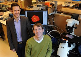
Prof Jonathan Coleman (left) pictured with CRANN Director, Prof John Boland

Prof Jonathan Coleman (left) pictured with CRANN Director, Prof John Boland
This research can be compared to the work regarding the two-dimensional material graphene, which won the Nobel Prize in 2010. Graphene has generated significant interest because when separated into individual flakes, it has exceptional electronic and mechanical properties that are very different to those of its parent crystal, graphite. However, graphite is just one of hundreds of layered materials, some of which may enable powerful new technologies.

Coleman's work will open up over 150 similarly exotic layered materials – such as Boron Nitride, Molybdenum disulfide, and Bismuth telluride – that have the potential to be metallic, semiconducting or insulating, depending on their chemical composition and how their atoms are arranged. This new family of materials opens a whole range of new "super" materials.

For decades researchers have tried to create nanosheets from layered materials in order to unlock their unusual electronic and thermoelectric properties. However, previous methods were time consuming, laborious or of very low yield and so unsuited to most applications.

"Our new method offers low-costs, a very high yield and a very large throughput: within a couple of hours, and with just 1 mg of material, billions and billions of one-atom-thick nanosheets can be made at the same time from a wide variety of exotic layered materials," explained Dr Nicolosi, from the University of Oxford.

These new materials are also suited for use in next generation batteries – "supercapacitors" – which can deliver energy thousands of times faster than standard batteries, enabling new applications such as electric cars. Many of these new atomic layered materials are very strong and can be added to plastics to produce super-strong composites. These will be useful in a range of industries from simple structural plastics to aeronautics.

###

*Other collaborators in the research were Korea University, Texas A &M University, Imperial College London
*The research paper titled ‘Two-dimensional nanosheets produced by liquid exfoliation of layered materials’, is published in the 4 February edition of the journal Science.

Contact: Professor Jonathan Coleman colemaj@tcd.ie 003-538-778-34917 Trinity College Dublin

Sunday, February 27, 2011

A new record for Tyndall's revolutionary microchip technology VIDEO


Last February, Nature Nanotechnology announced the development at UCC's Tyndall National Institute of the world's first junctionless transistor. The transistor is the building block of the microchip and the breakthrough by Professor Jean-Pierre Colinge, was greeted by the semiconductor industry as a major advance. Now, Professor Colinge is back in the news with a transistor that is reduced again by a factor of twenty. To put in it context, his latest innovation is 2000 times smaller than a strand of human hair, 30 per cent more energy efficient than existing transistors and gives a better performance than transistors now on the market! With up to two billion transistors on a single microchip, the latest breakthrough will help to drive more simple manufacturing processes and is again being viewed as a significant leap forward. Professor Colinge explains:

TEXT and VIDEO CREDIT: UCCIreland

Saturday, February 26, 2011

NIST technique controls sizes of nanoparticle clusters for EHS studies

The same properties that make engineered nanoparticles attractive for numerous applications—small as a virus, biologically and environmentally stabile, and water-soluble—also cause concern about their long-term impacts on environmental health and safety (EHS). One particular characteristic, the tendency for nanoparticles to clump together in solution, is of great interest because the size of these clusters may be key to whether or not they are toxic to human cells. Researchers at the National Institute of Standards and Technology (NIST) have demonstrated for the first time a method for producing nanoparticle clusters in a variety of controlled sizes that are stable over time so that their effects on cells can be studied properly.*

In their tests, the NIST team made samples of gold, silver, cerium oxide and positively-charged polystyrene nanoparticles and suspended them separately in cell culture medium, allowing clumping to occur in each. They stopped the clumping by adding a protein, bovine serum albumin (BSA), to the mixtures. The longer the nanoparticles were allowed to clump together, the larger the size of the resulting cluster. For example, a range of clustering times using 23 nanometer silver nanoparticles produced a distribution of masses between 43 and 1,400 nanometers in diameter. Similar size distributions for the other three nanoparticle types were produced using this method.

Nanoparticle Clusters

Caption: Transmission electron micrograph of gold nanoparticles clustering in solution. The distance between the two red arrows is approximately 280 nanometers, some 200 times smaller than the diameter of a human hair. The individual nanoparticles are approximately 15 nanometers in diameter, about the distance across 40 side-by-side sodium atoms.

Credit: A. Keene, US Food and Drug Administration. Usage Restrictions: None.
The researchers learned that using the same "freezing times"—the points at which BSA was added to halt the process—yielded consistent size distributions for all four nanoparticle types. Additionally, all of the BSA-controlled dispersions remained stable for 2-3 days, which is sufficient for many toxicity studies.

Having successfully shown that they could control the production of nanoparticle clumps of different sizes, the researchers wanted next to prove that their creations could be put to work. Different-sized silver nanoparticle clusters were mixed with horse blood in an attempt to study the impact of clumping size on red blood cell toxicity. The presence of hemoglobin, the iron-based molecule in red blood cells that carries oxygen, would tell researchers if the cells had been lysed (broken open) by silver ions released into the solution from the clusters.
In turn, measuring the amount of hemoglobin in solution for each cluster size would define the level of toxicity—possibly related to the level of silver ion release—for that specific average size.

What the researchers found was that red blood cell destruction decreased as cluster size increased. They hypothesize that large nanoparticle clusters dissolve more slowly than small ones, and therefore, release fewer silver ions into solution.

In the future, the NIST team plans to further characterize the different cluster sizes achievable through their production method, and then use those clusters to study the impact on cytotoxicity of coatings (such as polymers) applied to the nanoparticles.

###

* J.M. Zook, R.I. MacCuspie, L.E. Locascio, M.D. Halter and J.T. Elliott. Stable nanoparticle aggregates/agglomerates of different sizes and the effect of their size on hemolytic cytotoxicity. Nanotoxicology, published online Dec. 13, 2010 (DOI: 10.3109/17435390.2010.536615).

Contact: Michael E. Newman michael.newman@nist.gov 301-975-3025 National Institute of Standards and Technology (NIST)

Friday, February 25, 2011

Engineered cells could usher in programmable cell therapies

Researchers at BWH have engineered cells that could solve one of the key challenges associated with the procedure: Control of the cells and their microenvironment following transplantation.

Boston, MA - In work that could jumpstart the promising field of cell therapy, in which cells are transplanted into the body to treat a variety of diseases and tissue defects, researchers at Brigham and Women's Hospital (BWH) have engineered cells that could solve one of the key challenges associated with the procedure: control of the cells and their microenvironment following transplantation.

In the work, reported in the journal Biomaterials on January 26, the team reports creating tiny internal depots within human mesenchymal adult stem cells, which among other functions are key to the generation of several tissues. These depots can slowly release a variety of agents to influence the behavior of not only the cells containing the depots, but also those close to them and even much farther away. The team demonstrated this by prompting mesenchymal stem cells to differentiate into the cells that make bone.

"This work could allow programmable cell therapies where the cell or the agent is the therapeutic," says Jeffrey Karp, leader of the work and co-director of the Center for Regenerative Therapeutics (ReGen Rx) at BWH. "For example, depots containing specific agents could enhance cell survival or expression of a particular growth factor. Cells could also be used as a delivery vehicle to shuttle drugs to target tissues that may be useful to accelerate tissue regeneration, or to deliver chemotherapeutics to tumors while minimizing systemic side effects."

Jeffrey Karp, James A. Ankrum, Brigham and Women's Hospital

Caption: Researchers at Brigham and Women's Hospital have engineered human mesenchymal adult stem cells (one cell shown, in red) to contain tiny depots (green) that can influence the behavior of the cells and those surrounding them, including their survival, differentiation, or production of a therapeutic protein. Left is Jeffrey Karp, co-director of the Center for Regenerative Therapeutics at Brigham & Women's Hospital, right is James A. Ankrum, co-first author on the paper and an HST graduate student. Not shown: Debanjan Sarkar, also a co‑first author of the paper, now at the University of Buffalo.

Credit: Photo by Donna Coveney. Usage Restrictions: None.

Stem Cells

Caption: Researchers at Brigham and Women's Hospital have engineered human mesenchymal adult stem cells (one cell shown, in red) to contain tiny depots (green) that can influence the behavior of the cells and those surrounding them, including their survival, differentiation, or production of a therapeutic protein.

Credit: Image courtesy Karp lab, Brigham and Women's Hospital. Usage Restrictions: None.
Toward Cell Therapy

"Ten to fifteen years from now, people will visit cell infusion centers to receive routine therapy for multiple diseases and tissue defects," predicts Karp, who also holds appointments through Harvard Medical School, Harvard Stem Cell Institute, and the Harvard-MIT Division of Health Sciences and Technology (HST). For example, a person who has had a heart attack could be infused with cells that could help stimulate regeneration of new heart cells to replace those that have died and prevent eventual heart failure.

Today, however, there is only one cell therapy that has saved tens of thousands of lives: bone marrow transplantation. In this procedure healthy blood stem cells home in to the bone marrow to regenerate the blood system of cancer patients following bone marrow ablation through chemotherapy or radiation.

One of the reasons for the lack of success of other cell therapies is the inability to control the cells and the host's response following transplantation, says Karp. "We can exhibit exquisite control over cells in a [laboratory] dish—we can get them to do whatever we want. But when we transplant them into the body, their fate and function are at the mercy of the biological milieu. We typically lose complete control and this prevents us from achieving the promise of cell therapy."

There are ways to get around this problem, but they have limitations. For example, cells can be put on a scaffold or biomaterial that releases drugs or other agents that affect their behavior. The cells, however, have to stay in close proximity to the material to be impacted by the agents. Cells can also be genetically modified with viruses to produce agents that will influence their behavior, but this has potential safety concerns.

Natural Inspiration

The Karp team was inspired by the natural ability of many proteins and other agents to be transported in and out of cells. They already knew that cells could internalize the tiny synthetic particles used in the controlled delivery of drugs—could these particles be used in cell therapy?

To find out, the researchers developed biodegradable particles about ten times smaller than a mesenchymal stem cell (MSC).
They loaded these particles with a dye, placed them near living MSCs, and found that the cells did indeed internalize them without immediately spitting them out. "Initially, this was a major challenge," comments James A. Ankrum, co-first author on the paper and an HST graduate student. "The particles needed to be small enough for the cells to internalize, yet large enough to prevent being shed by the cell." The dye was observed to seep from the tiny particle depots to the outside of the cell through the cell membrane over a period of several days.

Next, they replaced the dye with an agent known to spur MSCs to differentiate into osteoblasts, the cells that make bone. They found that not only did MSCs containing the depots differentiate into osteoblasts, but so did MSCs without depots that were nearby and even much further away. "We demonstrated that the fate of particle-carrying cells could be controlled, as well as the fates of neighboring and distant cells," says Debanjan Sarkar, co-first author of the paper and now a professor at the University of Buffalo.

Additional authors are Grace S. L. Teo of HST and Christopher V. Carman of Beth Israel Deaconess Hospital.

To date the team has demonstrated the engineered cells in laboratory systems designed to mimic the body. They are in the process of translating the work to animals. "If it works in vivo, it could have a significant impact globally on cell therapy," says Karp, whose team has filed for a patent on the work.

###

This work was funded by the National Institutes of Health, the American Heart Association, and the National Science Foundation.

Contact: Holly Brown-Ayers hbrown-ayers@partners.org 617-534-1603 Brigham and Women's Hospital

Thursday, February 24, 2011

Tuning graphene film so it sheds water

Windshields that shed water so effectively that they don’t need wipers. Ship hulls so slippery that they glide through the water more efficiently than ordinary hulls.

These are some of the potential applications for graphene, one of the hottest new materials in the field of nanotechnology, raised by the research of James Dickerson, assistant professor of physics at Vanderbilt.

Dickerson and his colleagues have figured out how to create a freestanding film of graphene oxide and alter its surface roughness so that it either causes water to bead up and run off or causes it to spread out in a thin layer.

“Graphene films are transparent and, because they are made of carbon, they are very inexpensive to make,” Dickerson said. “The technique that we use can be rapidly scaled up to produce it in commercial quantities.”

His approach is documented in an article published online by the journal ACSNano on Nov. 26.

Graphene is made up of sheets of carbon atoms arranged in rings –d> something like molecular chicken wire. Not only is this one of the thinnest materials possible, but it is 10 times stronger than steel and conducts electricity better at room temperature than any other known material. Graphene’s exotic properties have attracted widespread scientific interest, but Dickerson is one of the first to investigate how it interacts with water.

Physicist James Dickerson, left, and graduate student Saad Hasan

Physicist James Dickerson, left, and graduate student Saad Hasan (Photo by Daniel Dubois)
Many scientists studying graphene make it using a dry method, called “mechanical cleavage,” that involves rubbing or scraping graphite against a hard surface. The technique produces sheets that are both extremely thin and extremely fragile. Dickerson’s method can produce sheets equally as thin but considerably stronger than those made by other techniques. It is already used commercially to produce a variety of different coatings and ceramics. Known as electrophoretic deposition, this “wet” technique combines an electric field within a liquid medium to create nanoparticle films that can be transferred to another surface.

Dickerson and his colleagues found that they could change the manner in which the graphene oxide particles assemble into a film by varying the pH of the liquid medium and the electric voltage used in the process. One pair of settings lay down the particles in a “rug” arrangement that creates a nearly atomically smooth surface. A different pair of settings causes the particles to clump into tiny “bricks” forming a bumpy and uneven surface. The researchers determined that the rug surface causes water to spread out in a thin layer, while the brick surface causes water to bead up and run off.

Dickerson is pursuing an approach that could create film that enhances these water-associated properties, making them even more effective at either spreading out water or causing it to bead up and run off. There is considerable academic and commercial interest in the development of coatings with these enhanced properties, called super-hydrophobic and super-hydrophilic. Potential applications range from self-cleaning glasses and clothes to antifogging surfaces to corrosion protection and snow-load protection on buildings. However, effective, low-cost and durable coatings have yet to make it out of the laboratory.

Dickerson’s idea is to apply his basic procedure to “fluorographene” – a fluorinated version of graphene that is a two-dimensional version of Teflon – recently produced by Kostya S. Novoselov and Andre K. Geim at the University of Manchester, who received the 2010 Nobel Prize for the discovery of graphene. Normal fluorographene under tension should be considerably more effective in repelling water than graphene oxide. So there is a good chance a “brick” version and a “rug” version would have extreme water-associated effects, Dickerson figures.

Graduate students Saad Hasan, John Rigueur, Robert Harl and Alex Krejci, postdoctoral research scientist Isabel Gonzalo-Juan and Associate Professor of Chemical and Biomolecular Engineering Bridget R. Rogers contributed to the research, which was funded by a Vanderbilt Discovery grant and by the National Science Foundation.

Contact: David F. Salisbury david.salisbury@vanderbilt.edu 615-343-6803 Vanderbilt University

Wednesday, February 23, 2011

What a ride! Researchers take molecules for a spin VIDEO

Rice University scientists model tiny rotors, key to future nanomachines

"This is no cartoon. It's a real molecule, with all the interactions taking place correctly," said Anatoly Kolomeisky as he showed an animation of atoms twisting and turning about a central hub like a carnival ride gone mad.

Kolomeisky, a Rice University associate professor of chemistry, was offering a peek into a molecular midway where atoms dip, dive and soar according to a set of rules he is determined to decode.

Kolomeisky and Rice graduate student Alexey Akimov have taken a large step toward defining the behavior of these molecular whirligigs with a new paper in the American Chemical Society's Journal of Physical Chemistry C. Through molecular dynamics simulations, they defined the ground rules for the rotor motion of molecules attached to a gold surface.

It's an extension of their work on Rice's famed nanocars, developed primarily in the lab of James Tour, Rice's T.T. and W.F. Chao Chair in Chemistry as well as a professor of mechanical engineering and materials science and of computer science, but for which Kolomeisky has also constructed molecular models.

Alexey Akimov Anatoly Kolomeisky

CAPTION: Rice graduate student Alexey Akimov, left, and Anatoly Kolomeisky, associate professor of chemistry, have taken a large step toward defining the behavior of molecules attached to a gold surface. (Credit Jeff Fitlow/Rice University)
Striking out in a different direction, the team has decoded several key characteristics of these tiny rotors, which could harbor clues to the ways in which molecular motors in human bodies work.

The motion they described is found everywhere in nature, Kolomeisky said. The most visible example is in the flagella of bacteria, which use a simple rotor motion to move. "When the flagella turn clockwise, the bacteria move forward. When they turn counterclockwise, they tumble." On an even smaller level, ATP-synthase, which is an enzyme important to the transfer of energy in the cells of all living things, exhibits similar rotor behavior -- a Nobel Prize-winning discovery.

Understanding how to build and control molecular rotors, especially in multiples, could lead to some interesting new materials in the continuing development of machines able to work at the nanoscale, he said. Kolomeisky foresees, for instance, radio filters that would let only a very finely tuned signal pass, depending on the nanorotors' frequency.


"It would be an extremely important, though expensive, material to make," he said. "But if I can create hundreds of rotors that move simultaneously under my control, I will be very happy."

The professor and his student cut the number of parameters in their computer simulation to a subset of those that most interested them, Kolomeisky said. The basic-model molecule had a sulfur atom in the middle, tightly bound to a pair of alkyl chains, like wings, that were able to spin freely when heated. The sulfur anchored the molecule to the gold surface.

While working on a previous paper with researchers at Tufts University, Kolomeisky and Akimov saw photographic evidence of rotor motion by scanning tunneling microscope images of sulfur/alkyl molecules heated on a gold surface. As the heat rose, the image went from linear to rectangular to hexagonal, indicating motion. What the pictures didn't indicate was why.

That's where computer modeling was invaluable, both on the Kolomeisky lab's own systems and through Rice's SUG@R platform, a shared supercomputer cluster. By testing various theoretical configurations -- some with two symmetrical chains, some asymmetrical, some with only one chain -- they were able to determine a set of interlocking characteristics that control the behavior of single-molecule rotors.

First, he said, the symmetry and structure of the gold surface material (of which several types were tested) has a lot of influence on a rotor's ability to overcome the energy barrier that keeps it from spinning all the time. When both arms are close to surface molecules (which repel), the barrier is large. But if one arm is over a space -- or hollow -- between gold atoms, the barrier is significantly smaller.

Second, symmetric rotors spin faster than asymmetric ones. The longer chain in an asymmetric pair takes more energy to get moving, and this causes an imbalance. In symmetric rotors, the chains, like rigid wings, compensate for each other as one wing dips into a hollow while the other rises over a surface molecule.

Third, Kolomeisky said, the nature of the chemical bond between the anchor and the chains determines the rotor's freedom to spin.

Finally, the chemical nature of rotating groups is also an important factor.

Kolomeisky said the research opens a path for simulating more complex rotor molecules. The chains in ATP-synthase are far too large for a simulation to wrangle, "but as computers get more powerful and our methods improve, we may someday be able to analyze such long molecules," he said.

###

The Welch Foundation, the National Science Foundation and the National Institutes of Health funded the research.

Located in Houston, Rice University is consistently ranked among the nation's top 20 universities by U.S. News & World Report. A Tier One research university known for its "unconventional wisdom," Rice has schools of Architecture, Business, Continuing Studies, Engineering, Humanities, Music, Natural Sciences and Social Sciences and offers its 3,485 undergraduates and 2,275 graduate students a wide range of majors. Rice has the sixth-largest endowment per student among American private research universities and is rated No. 4 for "best value" among private universities by Kiplinger's Personal Finance. Its undergraduate student-to-faculty ratio is less than 6-to-1. With a residential college system that builds close-knit and diverse communities and collaborative culture, Rice has been ranked No. 1 for best quality of life multiple times by the Princeton Review.

Contact: David Ruth druth@rice.edu 713-348-6327 Rice University

NIDEO CREDIT: RiceUniversity

Tuesday, February 22, 2011

New transistors: An alternative to silicon and better than graphene

Smaller and more energy-efficient electronic chips could be made using molybdenite, a material developed in Switzerland.

Smaller and more energy-efficient electronic chips could be made using molybdenite. In an article appearing online January 30 in the journal Nature Nanotechnology, EPFL's Laboratory of Nanoscale Electronics and Structures (LANES) publishes a study showing that this material has distinct advantages over traditional silicon or graphene for use in electronics applications.

A discovery made at EPFL could play an important role in electronics, allowing us to make transistors that are smaller and more energy efficient. Research carried out in the Laboratory of Nanoscale Electronics and Structures (LANES) has revealed that molybdenite, or MoS2, is a very effective semiconductor. This mineral, which is abundant in nature, is often used as an element in steel alloys or as an additive in lubricants. But it had not yet been extensively studied for use in electronics.

100,000 times less energy

"It's a two-dimensional material, very thin and easy to use in nanotechnology. It has real potential in the fabrication of very small transistors, light-emitting diodes (LEDs) and solar cells," says EPFL Professor Andras Kis, whose LANES colleagues M. Radisavljevic, Prof. Radenovic et M. Brivio worked with him on the study. He compares its advantages with two other materials: silicon, currently the primary component used in electronic and computer chips, and graphene, whose discovery in 2004 earned University of Manchester physicists André Geim and Konstantin Novoselov the 2010 Nobel Prize in Physics.

Transistor with MoS2

Caption: This is a digital model showing how molybdenite can be integrated into a transistor.

Credit: Credit: EPFL. Usage Restrictions: With Mention.
One of molybdenite's advantages is that it is less voluminous than silicon, which is a three-dimensional material. "In a 0.65-nanometer-thick sheet of MoS2, the electrons can move around as easily as in a 2-nanometer-thick sheet of silicon," explains Kis. "But it's not currently possible to fabricate a sheet of silicon as thin as a monolayer sheet of MoS2." Another advantage of molybdenite is that it can be used to make transistors that consume 100,000 times less energy in standby state than traditional silicon transistors. A semi-conductor with a "gap" must be used to turn a transistor on and off, and molybdenite's 1.8 electron-volt gap is ideal for this purpose.

Better than graphene

In solid-state physics, band theory is a way of representing the energy of electrons in a given material. In semi-conductors, electron-free spaces exist between these bands, the so-called "band gaps." If the gap is not too small or too large, certain electrons can hop across the gap. It thus offers a greater level of control over the electrical behavior of the material, which can be turned on and off easily.

The existence of this gap in molybdenite also gives it an advantage over graphene. Considered today by many scientists as the electronics material of the future, the "semi-metal" graphene doesn't have a gap, and it is very difficult to artificially reproduce one in the material.

###

Contact: Michael Mitchell michael.mitchell@epfl.ch 41-798-103-107 Ecole Polytechnique Fédérale de Lausanne

New super strength Nanotechnology Meaning of Information Technology Bad Robot VIDEO


New super strength Nanotechnology, Meaning of Information Technology Bad Robot Commercial VIDEO

20 second commercial I (pauljharris) made for MIT class at CU (Radio 1190, the University of Colorado at Boulder's station).

VIDEO and TEXT CREDIT: pauljharris

Monday, February 21, 2011

Nanowires exhibit giant piezoelectricity

Gallium nitride (GaN) and zinc oxide (ZnO) are among the most technologically relevant semiconducting materials. Gallium nitride is ubiquitous today in optoelectronic elements such as blue lasers (hence the blue-ray disc) and light-emitting-diodes (LEDs); zinc oxide also finds many uses in optoelectronics and sensors.

In the past few years, though, nanostructures made of these materials have shown a plethora of potential functionalities, ranging from single-nanowire lasers and LEDs to more complex devices such as resonators and, more recently, nanogenerators that convert mechanical energy from the environment (body movements, for example) to power electronic devices. The latter application relies on the fact that GaN and ZnO are also piezoelectric materials, meaning that they produce electric charges as they are deformed.

In a paper published online in the journal Nano Letters, Horacio Espinosa, the James N. and Nancy J. Farley Professor in Manufacturing and Entrepreneurship at the McCormick School of Engineering and Applied Science at Northwestern University, and Ravi Agrawal, a graduate student in Espinosa's lab, reported that piezoelectricity in GaN and ZnO nanowires is in fact enhanced by as much as two orders of magnitude as the diameter of the nanowires decrease.

Horacio Espinosa

Horacio Espinosa
"This finding is very exciting because it suggests that constructing nanogenerators, sensors and other devices from smaller nanowires will greatly improve their output and sensitivity," Espinosa said.

"We used a computational method called Density Functional Theory (DFT) to model GaN and ZnO nanowires of diameters ranging from 0.6 nanometers to 2.4 nanometers," Agrawal said. The computational method is able to predict the electronic distribution of the nanowires as they are deformed and, therefore, allows calculating their piezoelectric coefficients.

The researchers' results show that the piezoelectric coefficient in 2.4 nanometer-diameter nanowires is about 20 times larger and about 100 times larger for ZnO and GaN nanowires, respectively, when compared to the coefficient of the materials at the macroscale.
This confirms previous computational findings on ZnO nanostructures that showed a similar increase in piezoelectric properties. However, calculations for piezoelectricity of GaN nanowires as a function of size were carried out in this work for the first time, and the results are clearly more promising as GaN shows a more prominent increase.

"Our calculations reveal that the increase in piezoelectric coefficient is a result of the redistribution of electrons in the nanowire surface, which leads to an increase in the strain-dependent polarization with respect to the bulk materials," Espinosa said.

The findings by Espinosa and Agrawal may have important implications for the field of energy harvesting as well as for fundamental science. For energy harvesting, where piezoelectric elements are used to convert mechanical to electrical energy in order to power electronic devices, these results point to an advantage in reducing the size of the piezoelectric elements down to the nanometer scale. Energy harvesting devices built from small-diameter nanowires should in principle be able to produce more electrical energy from the same amount of mechanical energy than their bulk counterparts.

In terms of fundamental science, these results further previous conclusions that matter at the nanoscale has different properties. It is clear now that by tailoring the size of nanostructures, their mechanical, electrical and thermal properties can be tuned as well.

"Our focus remains on understanding the fundamental principles governing the behavior of nanostructures as a function of their size," Espinosa and Agrawal say. "One of the most important issues that needs to be addressed is to obtain experimental confirmation of these results, and establish up to what size the giant piezoelectric effects remain significant."

Espinosa and Agrawal hope their work will spur new interest in the electromechanical properties of nanostructures, both from theoretical and experimental standpoints, in order to clear the path for the design and optimization of future nanoscale devices.

###

Contact: Megan Fellman fellman@northwestern.edu 847-491-3115 Northwestern University

Sunday, February 20, 2011

The Future Of Carbon Nanotubes (Intelligent Investing With Steve Forbes) VIDEO


Tech guru George Gilder on water filtration, space exploration and great expectations for nanotechnology.

VIDEO CREDIT: forbes

Physicists take new look at the atom

Measuring the attractive forces between atoms and surfaces with unprecedented precision, University of Arizona physicists have produced data that could refine our understanding of the structure of atoms and improve nanotechnology. The discovery has been published in the journal Physical Review Letters.

Van der Waals forces are fundamental for chemistry, biology and physics. However, they are among the weakest known chemical interactions, so they are notoriously hard to study. This force is so weak that it is hard to notice in everyday life. But delve into the world of micro-machines and nano-robots, and you will feel the force – everywhere.

"If you make your components small enough, eventually this van-der-Waals potential starts to become the dominant interaction," said Vincent Lonij, a graduate student in the UA department of physics who led the research as part of his doctoral thesis.

"If you make tiny, tiny gears for a nano-robot, for example, those gears just stick together and grind to a halt. We want to better understand how this force works."

To study the van-der-Waals force, Lonij and his co-workers Will Holmgren, Cathy Klauss and associate professor of physics Alex Cronin designed a sophisticated experimental setup that can measure the interactions between single atoms and a surface. The physicists take advantage of quantum mechanics, which states that atoms can be studied and described both as particles and as waves.

Atom-beam Chamber

Caption: Graduate student Vincent Lonij (left), associate professor of physics Alex Cronin, research assistant Will Holmgren and undergraduate student Catherine Klauss perform maintenance on a chamber used to beam atoms through a grating to measure a tiny force that helps physicists better understand the structure of atoms.

Credit: Norma Jean Gargasz/UANews. Usage Restrictions: Usage only granted in conjunction with reporting/posting of the news release.
"We shoot a beam of atoms through a grating, sort of like a micro-scale picket fence," Lonij explained. "As the atoms pass through the grating, they interact with the surface of the grating bars, and we can measure that interaction."

As the atoms pass through the slits in the grating, the van-der-Waals force attracts them to the bars separating the slits. Depending on how strong the interaction, it changes the atom's trajectory, just like a beam of light is bent when it passes through water or a prism.

A wave passing through the middle of the slit does so relatively unencumbered. On the other hand, if an atom wave passes close by the slit's edges, it interacts with the surface and skips a bit ahead, "out of phase," as physicists say.

"After the atoms pass through the grating, we detect how much the waves are out of phase, which tells us how strong the van-der-Waals potential was when the atoms interacted with the surface."

Mysterious as it seems, without the van-der-Waals force, life would be impossible. For example, it helps the proteins that make up our bodies to fold into the complex structures that enable them to go about their highly specialized jobs.

Unlike magnetic attraction, which affects only metals or matter carrying an electric current, van-der-Waals forces make anything stick to anything, provided the two are extremely close to each other. Because the force is so weak, its action doesn't range beyond the scale of atoms – which is precisely the reason why there is no evidence of such a force in our everyday world and why we leave it to physicists such as Lonij to unravel its secrets.

Initially, he was driven simply by curiosity, Lonij said. When he started his project, he didn't know it would lead to a new way of measuring the forces between atoms and surfaces that may change the way physicists think about atoms.

And with a smile, he added, "I thought it would be fitting to study this force, since I am from the Netherlands; Mr. van der Waals was Dutch, too."

In addition to proving that core electrons contribute to the van-der-Waals potential, Lonij and his group made another important discovery.

Physicists around the world who are studying the structure of the atom are striving for benchmarks that enable them to test their theories about how atoms work and interact. "Our measurements of atom-surface potentials can serve as such benchmarks," Lonij explained. "We can now test atomic theory in a new way."

Studying how atoms interact is difficult because they are not simply tiny balls. Instead, they are what physicists call many-body systems. "An atom consists of a whole bunch of other particles, electrons, neutrons, protons, and so forth," Lonij said.

Even though the atom as a whole holds no net electric charge, the different charged particles moving around in its interior are what create the van-der-Waals force in the first place.

"What happens is that the electrons, which hold all the negative charge, and the protons, which hold all the positive charge, are not always in the same places. So you can have tiny little differences in charge that are fluctuating very fast. If you put a charge close to a surface, you induce an image charge. In a highly simplified way, you could say the atom is attracted to its own reflection."

To physicists, who prefer things neat and clean and tractable with razor-sharp mathematics, such a system, made up from many smaller particles zooming around each other, is difficult to pin down. To add to the complication, most surfaces are not clean. As Lonij puts it, "Comparing such a dirty system to theory is a big challenge, but we figured out a way to do it anyway."

"A big criticism of this type of work always was, 'well, you're measuring this atom-surface potential, but you don't know what the surface looks like so you don't know what you're really measuring.'"

To eliminate this problem, Lonij's team used different types of atoms and looked at how each interacted with the same surface.

"Our technique gives you the ratio of potentials directly without ever knowing the potential for either of the two atoms," he said. "When I started five years ago, the uncertainty in these types of measurements was 20 percent. We brought it down to two percent."

The most significant discovery was that an atom's inner electrons, orbiting the nucleus at a closer range than the atom's outer electrons, influence the way the atom interacts with the surface.

"We show that these core electrons contribute to the atom-surface potential," Lonij said, "which was only known in theory until now. This is the first experimental demonstration that core electrons affect atom-surface potentials."

"But what is perhaps more important," he added, "is that you can also turn it around. We now know that the core electrons affect atom-surface potentials. We also know that these core electrons are hard to calculate in atomic theory. So we can use measurements of atom-surface potentials to make the theory better: The theory of the atom."

###

Contact: Daniel Stolte stolte@email.arizona.edu 520-626-4402 University of Arizona

Saturday, February 19, 2011

New lab-on-chip advance uses low-cost, disposable paper strips

WEST LAFAYETTE, Ind. - Researchers have invented a technique that uses inexpensive paper to make "microfluidic" devices for rapid medical diagnostics and chemical analysis.

The innovation represents a way to enhance commercially available diagnostic devices that use paper-strip assays like those that test for diabetes and pregnancy.

"With current systems that use paper test strips you can measure things like pH or blood sugar, but you can't perform more complex chemical assays," said Babak Ziaie, a Purdue University professor of electrical and computer engineering and biomedical engineering. "This new approach offers the potential to extend the inexpensive paper-based systems so that they are able to do more complicated multiple analyses on the same piece of paper. It's a generic platform that can be used for a variety of applications.

Findings are detailed in a research paper published online this week in the journal Lab on a Chip.

Current lab-on-a-chip technology is relatively expensive because chips must be specifically designed to perform certain types of chemical analyses, with channels created in glass or plastic and tiny pumps and valves directing the flow of fluids for testing.

Microfluidic Devices

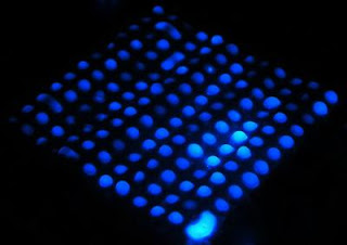
Caption: Researchers have invented a technique that uses inexpensive paper to make "microfluidic" devices for rapid medical diagnostics and chemical analysis. To demonstrate the new concept, the researchers created paper strips containing arrays of dots dipped in luminol, a chemical that turns fluorescent blue when exposed to blood. Blood was then sprayed on the strips, showing the presence of hemoglobin.

Credit: Birck Nanotechnology Center, Purdue University. Usage Restrictions: None.

lab-on-chip

Caption: Colored water is used to show how liquid wicks along tiny channels formed in paper using a laser, in research to develop a new technology for medical diagnostics and chemical analysis. Silica microparticles were deposited on patterned areas, allowing liquid to diffuse from one end of a channel to the other.

Credit: Birck Nanotechnology Center, Purdue University. Usage Restrictions: None.
The chips are being used for various applications in medicine and research, measuring specific types of cells and molecules in a patient's blood, monitoring microorganisms in the environment and in foods, and separating biological molecules for laboratory analyses. But the chips, which are roughly palm-size or smaller, are difficult to design and manufacture.

The new technique is simpler because the testing platform will be contained on a disposable paper strip containing patterns created by a laser. The researchers start with paper having a hydrophobic - or water-repellant - coating, such as parchment paper or wax paper used for cooking.

"We can buy this paper at any large discount retail store," Ziaie said. "These patterns can be churned out in the millions at very low cost."

A laser is used to burn off the hydrophobic coatings in lines, dots and patterns, exposing the underlying water-absorbing paper only where the patterns are formed.

"Since the hydrophobic agent is already present throughout the thickness of the paper, our method creates islands of hydrophilic patterns," Ziaie said. "This modified surface has a highly porous structure, which helps to trap and localize chemical and biological aqueous reagents for analysis. Furthermore, we've selectively deposited silica microparticles on patterned areas to allow diffusion from one end of a channel to the other."

Those microparticles help to wick liquid to a location where it would combine with another chemical, called a reactant, causing it to change colors and indicating a positive or negative test result.

Having a patterned hydrophilic surface is needed for many detection methods in biochemistry, such as enzyme-linked immunosorbent assay, or ELISA, used in immunology to detect the presence of an antibody or an antigen in a sample, Ziaie said.

To demonstrate the new concept, the researchers created paper strips containing arrays of dots dipped in luminol, a chemical that turns fluorescent blue when exposed to blood.

"Then we sprayed blood on the strips, showing the presence of hemoglobin," said Ziaie, whose research is based at the Birck Nanotechnology Center in the university's Discovery Park. "This is just a proof of concept."

Laser modification is known to alter the "wettability" of materials by causing structural and chemical changes to surfaces. However, this treatment has never before been done on paper, he said.

The researchers performed high-resolution imaging and spectroscopic analysis to study the mechanism behind the hydrophobic-hydrophilic conversion of laser-treated parchment paper.

The new approach is within a research area called paper microfluidics.

"Other techniques in paper microfluidics are more complicated," Ziaie said.

For example, other researchers have developed a method that lays down lines of wax or other hydrophobic material on top of untreated, hydrophilic paper.

"Our process is much easier because we just use a laser to create patterns on paper you can purchase commercially and it is already impregnated with hydrophobic material," Ziaie said. "It's a one-step process that could be used to manufacture an inexpensive diagnostic tool for the developing world where people can't afford more expensive analytical technologies."

The strips might be treated with chemicals that cause color changes when exposed to a liquid sample, with different portions of the pattern revealing specific details about the content of the sample. One strip could be used to conduct dozens of tests, he said.

The strips might be inserted into an electronic reader, similar to technology used in conventional glucose testers. Color changes would indicate the presence or absence of specific chemical compounds.

###

The research paper was written by graduate students Girish Chitnis, Zhenwen Ding and Chun-Li Chang; Cagri A. Savran, an associate professor of mechanical engineering, biomedical engineering and electrical and computer engineering; and Ziaie.

The National Science Foundation funded the work.

The researchers have patented the technique and it is available for licensing through Joseph Trebley, senior project manager for the Purdue Research Foundation Office of Technology Commercialization, at 765-588-3832, jptrebley@prf.org (www.prf.org/otc).

Writer: Emil Venere, 765-494-4709, venere@purdue.edu Source: Babak Ziaie, 765-494-0725, bziaie@purdue.edu Related website: Babak Ziaie: engineering.purdue.edu/ECE/People/profile

Contact: Emil Venere venere@purdue.edu 765-494-4709 Purdue University

Friday, February 18, 2011

New materials may bring advanced optical technologies, cloaking

WEST LAFAYETTE, Ind. - Researchers are developing a new class of "plasmonic metamaterials" as potential building blocks for advanced optical technologies, including ultrapowerful microscopes and computers, improved solar cells, and a possible invisibility cloak.

The new materials could make possible "nanophotonic" devices for numerous applications, said Alexandra Boltasseva, an assistant professor of electrical and computer engineering at Purdue University.

Unlike natural materials, metamaterials may possess an index of refraction less than one or less than zero. Refraction occurs as electromagnetic waves, including light, bend when passing from one material into another. It causes the bent-stick-in-water effect, which occurs when a stick placed in a glass of water appears crooked when viewed from the outside.

Being able to create materials with an index of refraction that's negative or between one and zero promises a range of potential breakthroughs in a new field called transformation optics. However, development of new technologies using metamaterials has been hindered by two major limitations: too much light is "lost," or absorbed by metals such as silver and gold contained in the metamaterials, and the materials need to be more precisely tuned so that they possess the proper index of refraction.

Transformation Optics

Caption: Researchers are developing a new class of "plasmonic metamaterials" as potential building blocks for advanced optical technologies and a range of potential breakthroughs in the field of transformation optics. This image shows the transformation optics "quality factor" for several plasmonic materials. For transformation optical devices, the quality factor rises as the amount of light "lost," or absorbed, by plasmonic materials falls, resulting in materials that are promising for a range of advanced technologies.

Credit: Birck Nanotechnology Center, Purdue University. Usage Restrictions: None.
Now, researchers are proposing a new approach to overcome these obstacles. Findings will be detailed in an article appearing Friday (Jan. 21) in the journal Science. The article was written by Boltasseva and Harry Atwater, Howard Hughes Professor and a professor of applied physics and materials science at the California Institute of Technology.

The researchers are working to replace silver and gold in materials that are created using two options: making semiconductors more metallic by adding metal impurities to them; or adding non-metallic elements to metals, in effect making them less metallic. Examples of these materials include aluminum oxides and titanium nitride, which looks like gold and is used to coat the domes of Russian churches.

Researchers have tested some of the new materials, demonstrating their optical properties and finding that they outperform silver and gold, in work based at the Birck Nanotechnology Center in Purdue's Discovery Park.

Plasmonic metamaterials are promising for various advances, including a possible "hyperlens" that could make optical microscopes 10 times more powerful and able to see objects as small as DNA;
advanced sensors; new types of light-harvesting systems for more efficient solar cells; computers and consumer electronics that use light instead of electronic signals to process information; and a cloak of invisibility.

Optical nanophotonic circuits might harness clouds of electrons called "surface plasmons" to manipulate and control the routing of light in devices too tiny for conventional lasers.

Some of the new materials are showing promise in uses involving near-infrared light, the range of the spectrum critical for telecommunications and fiberoptics. Other materials also might work for light in the visible range of the spectrum. The new materials might be tuned so that their refractive index is ideal for specific ranges of the spectrum, allowing their use for particular applications.

Future photonics technologies will revolve around new types of optical transistors, switches and data processors. Conventional computers transmit and process pieces of information in serial form, or one piece at a time. However, future computers may use parallel streams of data, resulting in much faster networks and computers.

###

The work has been funded by the U.S. Army Research Office. Writer: Emil Venere, 765-494-4709, venere@purdue.edu Source: Alexandra Boltasseva, 765-494-0301, aeb@purdue.edu Related website: Alexandra Boltasseva: engineering.purdue.edu/ECE/People/profile

Contact: Emil Venere venere@purdue.edu 765-494-4709 Purdue University

Thursday, February 17, 2011

GRIN plasmonics

A practical path to superfast computing, ultrapowerful optical microscopy and invisibility carpet-cloaking devices.

They said it could be done and now they've done it. What's more, they did it with a GRIN. A team of researchers with the U.S. Department of Energy (DOE)'s Lawrence Berkeley National Laboratory (Berkeley Lab) and the University of California, Berkeley, have carried out the first experimental demonstration of GRIN – for gradient index – plasmonics, a hybrid technology that opens the door to a wide range of exotic optics, including superfast computers based on light rather than electronic signals, ultra-powerful optical microscopes able to resolve DNA molecules with visible light, and "invisibility" carpet-cloaking devices.

Working with composites featuring a dielectric (non-conducting) material on a metal substrate, and "grey-scale" electron beam lithography, a standard method in the computer chip industry for patterning 3-D surface topographies, the researchers have fabricated highly efficient plasmonic versions of Luneburg and Eaton lenses. A Luneburg lens focuses light from all directions equally well, and an Eaton lens bends light 90 degrees from all incoming directions.

Luneburg Plasmonic Lens

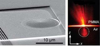
Caption: On the left is a scanning electron micrograph of a plasmonic Luneburg lens on a gold film. On the right, fluorescence imaging shows intensity of the SPPs propagated by the Luneburg lens (dotted circle). X marks the launching position of the electron beam and Z is the direction in which the SPPs propogate.

Credit: Image courtesy of Zhang group. Usage Restrictions: None.

Eaton Lens

Caption: On the left, a scanning electron micrograph of Eaton lenses on a gold film. On the right, fluorescence imaging shows the intensity of SPPs propagating in z-direction (arrow) and bending to the right when passing through the lens. The solid line marks the outer diameter of the lens and the dashed line marks the high index region.

Credit: Image courtesy of Zhang group. Usage Restrictions: None.
"This past year, we used computer simulations to demonstrate that with only moderate modifications of an isotropic dielectric material in a dielectric-metal composite, it would be possible to achieve practical transformation optics results," says Xiang Zhang, who led this research. "Our GRIN plasmonics technique provides a practical way for routing light at very small scales and producing efficient functional plasmonic devices."

Zhang, a principal investigator with Berkeley Lab's Materials Sciences Division and director of UC Berkeley's Nano-scale Science and Engineering Center (SINAM), is the corresponding author of a paper in the journal Nature Nanotechnology, describing this work titled, "Plasmonic Luneburg and Eaton Lenses." Co-authoring the paper were Thomas Zentgraf, Yongmin Liu, Maiken Mikkelsen and Jason Valentine.

GRIN plasmonics combines methodologies from transformation optics and plasmonics, two rising new fields of science that could revolutionize what we are able to do with light. In transformation optics, the physical space through which light travels is warped to control the light's trajectory, similar to the way in which outer space is warped by a massive object under Einstein's relativity theory. In plasmonics, light is confined in dimensions smaller than the wavelength of photons in free space, making it possible to match the different length-scales associated with photonics and electronics in a single nanoscale device.
"Applying transformation optics to plasmonics allows for precise control of strongly confined light waves in the context of two-dimensional optics," Zhang says. "Our technique is analogous to the well-known GRIN optics technique, whereas previous plasmonic techniques were realized by discrete structuring of the metal surface in a metal-dielectric composite."

Like all plasmonic technologies, GRIN plasmonics starts with an electronic surface wave that rolls through the conduction electrons on a metal. Just as the energy in a wave of light is carried in a quantized particle-like unit called a photon, so, too, is plasmonic energy carried in a quasi-particle called a plasmon. Plasmons will interact with photons at the interface of a metal and dielectric to form yet another quasi-particle, a surface plasmon polariton (SPP).

The Luneburg and Eaton lenses fabricated by Zhang and his co-authors interacted with SPPs rather than photons. To make these lenses, the researchers worked with a thin dielectric film (a thermplastic called PMMA) on top of a gold surface. When applying grey-scale electron beam lithography, the researchers exposed the dielectric film to an electron beam that was varied in dosage (charge per unit area) as it moved across the film's surface. This resulted in highly controlled differences in film thickness across the length of the dielectric that altered the local propagation of SPPs. In turn, the "mode index," which determines how fast the SPPs will propagate, is altered so that the direction of the SPPs can be influenced.

"By adiabatically tailoring the topology of the dielectric layer adjacent to the metal surface, we're able to continuously modify the mode index of SPPs," says Zentgraf. "As a result, we can manipulate the flow of SPPs with a greater degree of freedom in the context of two-dimensional optics."

Says Liu, "The practicality of working only with the purely dielectric material to transform SPPs is a big selling point for GRIN plasmonics. Controlling the physical properties of metals on the nanometer length-scale, which is the penetration depth of electromagnetic waves associated with SPPs extending below the metal surfaces, is beyond the reach of existing nanofabrication techniques."

Adds Zentgraf, "Our approach has the potential to achieve low-loss functional plasmonic elements with a standard fabrication technology that is fully compatible with active plasmonics."

In the Nature Nanotechnology paper, the researchers say that inefficiencies in plasmonic devices due to SPPs lost through scattering could be reduced even further by incorporating various SPP gain materials, such as fluorescent dye molecules, directly into the dielectric. This, they say, would lead to an increased propagation distance that is highly desired for optical and plasmonic devices. It should also enable the realization of two-dimensional plasmonic elements beyond the Luneburg and Eaton lenses.

Says Mikkelsen, "GRIN plasmonics can be immediately applied to the design and production of various plasmonic elements, such as waveguides and beam splitters, to improve the performance of integrated plasmonics. Currently we are working on more complex, transformational plasmonic devices, such as plasmonic collimators, single plasmonic elements with multiple functions, and plasmonic lenses with enhanced performance."

###

This research was supported by the U.S. Army Research Office and the National Science Foundation's Nano-scale Science and Engineering Center.

Lawrence Berkeley National Laboratory is a U.S. Department of Energy (DOE) national laboratory managed by the University of California for the DOE Office of Science. Berkeley Lab provides solutions to the world's most urgent scientific challenges including sustainable energy, climate change, human health, and a better understanding of matter and force in the universe. It is a world leader in improving our lives through team science, advanced computing, and innovative technology. Visit our Website at: www.lbl.gov

Contact: Lynn Yarris lcyarris@lbl.gov 510-486-5375 DOE/Lawrence Berkeley National Laboratory

Wednesday, February 16, 2011

Purdue team creates 'engineered organ' model for breast cancer research

WEST LAFAYETTE, Ind. - Purdue University researchers have reproduced portions of the female breast in a tiny slide-sized model dubbed "breast on-a-chip" that will be used to test nanomedical approaches for the detection and treatment of breast cancer.

The model mimics the branching mammary duct system, where most breast cancers begin, and will serve as an "engineered organ" to study the use of nanoparticles to detect and target tumor cells within the ducts.

Sophie Lelièvre, associate professor of basic medical sciences in the School of Veterinary Medicine, and James Leary, SVM Professor of Nanomedicine and professor of basic medical sciences in the School of Veterinary Medicine and professor of biomedical engineering in the Weldon School of Biomedical Engineering, led the team.

"Breast cancer is the most common cancer in women in most countries, and in the U.S. alone nearly 40,000 women lost their lives to it this past year," said Lelièvre, who is associate director of discovery groups in the Purdue Center for Cancer Research and a leader of the international breast cancer and nutrition project in the Oncological Sciences Center. "We've known that the best way to detect this cancer early and treat it effectively would be to get inside the mammary ducts to evaluate and treat the cells directly, and this is the first step in that direction."

Picture of 'Breast on-a-chip' Model

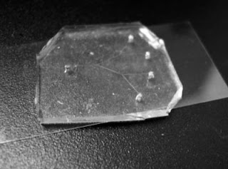
Caption: Purdue researchers' new model for breast cancer research, called "breast on-a-chip," mimics the branching mammary duct system.

Credit: Purdue University/Leary laboratory - Reproduced by permission of The Royal Society of Chemistry. Usage Restrictions: None.

3-D Rendering of New Model

Caption: This image shows a 3-D rendering of one of the channels lined with cells from a new model that will be used to test nanomedical approaches for the detection and treatment of breast cancer.

Credit: Purdue University/LeliÅvre laboratory - reproduced by permission of The Royal Society of Chemistry. Usage Restrictions: None.
Lelièvre and Leary hope eventually to be able to introduce magnetic nanoparticles through openings in the nipple, use a magnetic field to guide them through the ducts where they would attach to cancer cells and then reverse the magnetic field to retract any excess nanoparticles.

The nanoparticles could carry contrast agents to improve mammography, fluorescent markers to guide surgeons or anticancer agents to treat the cancer, Leary said.

"Nanoparticles can be designed to latch on to cancer cells and illuminate them, decreasing the size of a tumor that can be detected through mammography from 5 millimeters to 2 millimeters, which translates into finding the cancer 10 times earlier in its evolution," Leary said. "There also is great potential for nanoparticles to deliver anticancer agents directly to the cancer cells, eliminating the need for standard chemotherapy that circulates through the entire body causing harmful side effects."

Physicians have tried to access the mammary ducts through the nipple in the past, injecting fluid solutions to try to wash out cells that could be examined and used for a diagnosis of cancer. However, this approach could only reach the first third of the breast due to fluid pressure from the ducts, which branch and become smaller and smaller as they approach the glands that produce milk, Leary said.

"The idea is that nanoparticles with a magnetic core can float through the naturally occurring fluid in the ducts and be pulled by a magnet as opposed to being pushed with pressure," he said. "We think they could reach all the way to the back of the ducts, where it is believed most breast cancers originate.
Of course, we are only at the earliest stages and many tests need to be done."

Such tests could not be done using standard models that grow cells across a flat surface in a plastic dish, so the team created the artificial organlike model in which living cells line a three-dimensional replica of the smallest portions of the mammary ducts.

Leary is internationally known for his nanofabrication work using photolithography to build tiny, precise structures on thin pieces of silicon to create high-speed cell sorting and analysis tools. He used the same techniques to build a mold of branching channels out of a rubberlike material called polydimethylsiloxane. The channels are about 5 millimeters long of various diameters from 20 microns to 100 microns, roughly the diameter of a human hair, that match what is found near the end of the mammary duct system.

Lelièvre, whose group is one of the few in the world able to successfully grow the complicated cells that line the mammary ducts, coaxed the cells to grow within the mold and behave as they would within a real human breast.

"The cells within the breast ductal system have a very specific organization that has proven difficult to obtain in a laboratory," Lelièvre said. "The cells have different sides, and one side must face the wall of the duct and the other must face the inner channel. Reproducing this behavior is very challenging, and it had never been achieved on an artificial structure before."

The team coated the mold in a protein-based substance called laminin 111 as a foundation for the cells that allows them to attach to the mold and behave as they would inside the body, Lelièvre said.

Because injecting the delicate cells into the finished channels of the mold caused too much damage, the team created a removable top for the channels.

"The design of the U-shaped channels and top was necessary for us to be able to successfully apply the cells, but it also allows us to make changes quickly and easily for different tests," Lelièvre said. "We can easily introduce changes among the cells or insert a few tumor cells to test the abilities of the nanoparticles to recognize them. The design also makes it very easy to evaluate the results as the entire model fits under a microscope."

A paper detailing the team's work, which was funded by the U.S. Department of Defense, is published in the current issue of Integrative Biology. In addition to Lelièvre and Leary, co-authors include graduate student Meggie Grafton, research associate Lei Wang and postdoctoral researcher Pierre-Alexandre Vidi.

The team has demonstrated that nanoparticles can be moved within the bare channels of the mold filled with fluid, but has not yet moved nanoparticles through the finished model lined with living cells, Lelièvre said.

The team next plans to create and test nanoparticles with a slippery surface that will prevent them from sticking to the cells as they travel through the channels and coatings that contain antibodies to target and attach to specific types of cancerous and precancerous cells, she said.

"Although we are at the very beginning stages of this work, we are hopeful that this nanomedical approach will one day save lives and provide patients with an easier road to recovery," Lelièvre said. "The successful creation of this model is an important milestone in this work and it is a testament to what can be accomplished through multidisciplinary research." ###

Lelièvre and Leary are both members of the Purdue Center for Cancer Research and the Oncological Sciences Center. Leary also is a member of the Birck Nanotechnology Center and Bindley Bioscience Center at Purdue's Discovery Park.

Writer: Elizabeth K. Gardner, 765-494-2081, ekgardner@purdue.eduSources: Sophie Lelièvre, 765-496-7793, lelievre@purdue.edu James Leary, 765-494-7280, jfleary@purdue.edu Related Web sites: Purdue Center for Cancer Research: www.cancerresearch.purdue.edu/ Sophie Lelièvre: www.gradschool.purdue.edu/PULSe/faculty James Leary: www.purdue.edu/dp/mcf/

Contact: Elizabeth K. Gardner ekgardner@purdue.edu 765-494-2081 Purdue University

Tuesday, February 15, 2011

New microscopy method opens window on previously unseen cell features VIDEO

Despite the sophistication and range of contemporary microscopy techniques, many important biological phenomena still elude the precision of even the most sensitive tools. The need for refined imaging methods for fundamental research and biomedical applications related to the study of disease remains acute.

Nongjian (N.J.) Tao and his colleagues at the Biodesign Institute at Arizona State University have pioneered a new technique capable of peering into single cells and even intracellular processes with unprecedented clarity. The method, known as electrochemical impedance microscopy (EIM) may be used to explore subtle features of profound importance for basic and applied research, including cell adhesion, cell death (or apoptosis) and electroporation—a process that can be used to introduce DNA or drugs into cells.

This new investigative tool is expected to make significant research inroads, improving drug discovery for diseases like cancer, furthering the study of host cell-pathogen interactions, and refining the analysis of stem cell differentiation.

The group's research appears in today's issue of the journal Nature Chemistry.

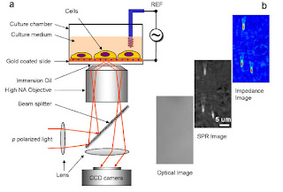
Electrical Impedance Microscopy

Figure 1: Electrical Impedance Microscopy
a) Schematic of the experimental setup. Laser light is directed onto a gold- coated slide through a layer of immersion oil, creating an SPR wave on the slide’s surface. When an electrical potential is induced in the culture medium, an EIM image of cell activity is created through signal changes in the SPR wave.
b) Silica particles measuring 200 nanometers across are imaged with EIM. The optical image lacks adequate spatial resolution to resolve the particles, while SPR and impedance images reveal them as bright spots.
As Tao explains, the method builds on the advantages of a powerful existing technology known as electrochemical impedance spectroscopy (EIS). Here, an AC voltage is applied to an electrode and the current response is measured as a change in impedance. (Impedance is defined as opposition to alternating current and extends the idea of electrical resistance to AC circuits.)

In addition to permitting observation of DNA, proteins, viruses and bacteria, EIS allows other subtle phenomena occurring at the electrode's surface to be imaged, including molecular binding events. Modifications of the EIS method have been applied to the study of other cellular processes including cell spreading, adhesion, invasion, toxicology and mobility.

A further attraction of the technique is that unlike fluorescence imaging, EIS is a so-called label-free technology, making it non-invasive to the sample under study. No fluorescent labeling particles or dyes—which can often interfere with normal cellular function—are required.
EIS however has one Achilles heel—it can't provide good spatial resolution. As Tao explains "Our technology provides high spatial resolution, making it possible to image and study single cells and subcellular processes, and detect and anayze biomolecules in a high density microarray format."


Video made with EIS showing the dynamic process of programmed cell death (apoptosis), comparing SPR and impedance images.


Video made with EIS showing electroporation of a cell. A voltage pulse causes a sudden increase in the plasma membrane’s permeability. Comparison of the EIM image shows significant detail not captured by SPR alone. The technique can be used to introduce drugs or DNA into a cell.

Obtaining good spatial resolution through conventional EIS would either require the use of multiple electrodes monitoring the surface to be studied, or a single electrode that mechanically scans across the surface. Both of these strategies have serious limitations that make them impractical. Tao and his colleagues have taken a different approach, combining EIS with another robust imaging technology based on surface plasmon resonance.

Surface plasmon resonance or SPR imaging is an optical detection process. Under proper conditions, polarized light striking a thin layer of gold, will cause free electrons to absorb the incident light particles, converting them into a surface plasmon wave, which propagates across the gold layer's surface, much like a wave on water. Perturbations of this delicate wave by target molecules cause alterations in the reflective properties of the incident light. These changes can be recorded and translated into an image.

Using SPR, simultaneous events over the entire surface of a biochip can be studied in real time, without the need for multiple electrodes. The method developed by Tao—known as electrochemical impedance microscopy (EIM)— differs from conventional EIS in that it does not measure current, but rather, uses plasmon resonance to detect impedance changes optically, dramatically enhancing spatial resolution of observed features. In addition to the EIM image, the new technique produces simultaneous optical and SPR imagery, which provide useful complementary information.

EIM allows for sub-micron spatial resolution of biological phenomena. Two cell processes in particular were observed in the current study: apoptosis and electroporation. Both of these phenomena require not only good spatial resolution but the ability to monitor fast-changing events in real time—something EIM excels at, using a specialized video camera to record rapid cellular events.

Apoptosis or cell death is of critical research significance. It is a central element in homeostasis and tissue/organ development. A better understanding of the cellular mechanisms of apoptosis is also critical for cancer research, and for the design of cancer therapies, which often attempt to induce apoptosis in malignant cells.

Tao and his group induced cell death in cervical cancer cells through the application of two molecules: MG132 and TRAIL—an apoptosis-inducing ligand. EIM imaging yielded detailed information of the successive stages of apoptosis, which include cellular shrinking and condensation followed by the fragmentation of nuclear material and eventual disintegration of the cells, with SPR and EIM imagery providing a complementary record of events. As Tao notes, before this study, such detailed information was only obtainable through fluorescent staining or electron microscopy.

Electroporation was also observed through EIM. Here, a voltage pulse is applied to a cell, causing a sudden increase in the conductivity and permeability the cell's plasma membrane. This valuable technique can be used to insert a molecular probe to monitor a cell's interior, or to introduce a cell-altering drug or segment of coding DNA. Once again, complementary information provided by optical, SPR and EIM combined to give a much more complete picture of this process, with the EIM images revealing the most dramatic changes over time. "We are excited by its potential for mapping out local activities of many celluar processes, such as ion channel activities and drug-cell interactions. "

Continued work will further refine this label-free, non-invasive microscopy technique, offering fresh insights into previously elusive cellular events. ###

Written by RIchard Harth Biodesign Institute science writer richard.harth@asu.edu

Contact: Joe Caspermeyer joseph.caspermeyer@asu.edu 480-727-0369 Arizona State University

Monday, February 14, 2011

easyJet tests nano technology for fuel efficiency VIDEO

easyJet, the UK's largest airline, today announced that it is the first commercial airline to trial a revolutionary nano-technology coating on its aircraft aimed at reducing drag and increasing fuel efficiency.

The ultra thin coating, already used on US military aircraft, is a polymer that cross links and bonds to the paint surface and only adds an estimated 4oz to the weight of the aircraft. The coating reduces the build up of debris on the aircraft's structure, leading edge and other surfaces; thus reducing drag on the surface of the aircraft. The manufacturers of the coating estimate that it could reduce easyJet's fuel consumption by 1-2%. The airline has coated eight aircraft and will compare their fuel consumption with the rest of the fleet during a 12 month trial period.

An easyJet passenger is responsible for 22% fewer emissions than a passenger on a traditional airline, when they fly the same route and use the same type of plane. Since its launch in 1995, easyJet has always strived to improve its efficiency to keep its costs down. Passengers benefit through low fares and a reduced carbon footprint.

This is achieved through a range of investments and innovations. easyJet's fleet of 194 aircraft, many with Tech Insertion engines, is one of the youngest in Europe averaging less than four years old.


It fills more of its seats than more than any scheduled European airline with a load factor of over 87%. easyJet planes taxi using one engine, use less ground equipment than legacy carriers and fly passengers to airports close to city centres, often with good public transport links. Weight onboard is reduced with light-weight carpets and the airline is currently looking at lighter seats in the cabin.

Carolyn McCall easyJet's CEO said: "easyJet is really pleased about the trial with the special coating on our aircraft. Efficiency is in easyJet's DNA. If we can find new ways of reducing the amount of fuel used by our aircraft we can pass the benefits onto our passengers by offering them low fares and a lower carbon footprint. All airlines should be incentivised to reduce the environmental impact of their operations which is why we welcome the government's commitment to move from APD to a fairer, greener per plane tax. We look forward to seeing the details of their proposal."

For more information please contact Sarah McIntyre in the easyJet Press Office: 01582 52 52 52/0779 88 38 332 press.office@easyJet.com

# The nano coating: The 'nano-technology' is a polymer that enables this high performance solution to cross link and bond with the surface materials to which it is being applied. It contains hard, durable acrylic elements and creates a perfectly smooth finish, filling the 'pores' of a surface with a unique resin. This forms a barrier to prevent penetration by contaminants of the 'hills and valleys' of a surface our eyes cannot see.

# Applying the coating: In the preparation solution a dicarboxylic acid a "cationic" (positive) polarizing wash is used to purge the pores of the surfaces to be treated and electrically charge the surface with a positive polarity. The pores are cleansed and charged and are ready to receive the unique "anionic" or negatively charged molecules of the emulsion. These molecules are pulled into the pores magnetically and held there, while all of the protective chemicals have cross-linked, bonded and cured, locking the coating into the paint and preventing drifting, fading or degradation of the paint until renewal.

# The coating is less than a micron thick when applied. A micron, short for micrometer, is a unit of measurement equal to one millionth of a meter.

# The special coating is applied and distributed in the UK by an organisation called TripleO

TripleO PR contact: Ross Thornley ross@tripleOps.com

VIDEO CREDIT: TheTVCGroup