Berkeley Lab scientists discover the edge states of graphene nanoribbons.
As far back as the 1990s, long before anyone had actually isolated graphene – a honeycomb lattice of carbon just one atom thick – theorists were predicting extraordinary properties at the edges of graphene nanoribbons. Now physicists at the U.S. Department of Energy's Lawrence Berkeley National Laboratory (Berkeley Lab), and their colleagues at the University of California at Berkeley, Stanford University, and other institutions, have made the first precise measurements of the "edge states" of well-ordered nanoribbons.
A graphene nanoribbon is a strip of graphene that may be only a few nanometers wide (a nanometer is a billionth of a meter). Theorists have envisioned that nanoribbons, depending on their width and the angle at which they are cut, would have unique electronic, magnetic, and optical features, including band gaps like those in semiconductors, which sheet graphene doesn't have.
"Until now no one has been able to test theoretical predictions regarding nanoribbon edge-states, because no one could figure out how to see the atomic-scale structure at the edge of a well-ordered graphene nanoribbon and how, at the same time, to measure its electronic properties within nanometers of the edge," says Michael Crommie of Berkeley Lab's Materials Sciences Division (MSD) and UC Berkeley's Physics Division, who led the research. "We were able to achieve this by studying specially made nanoribbons with a scanning tunneling microscope."

Caption: Graphene nanoribbons are narrow sheets of carbon atoms only one layer thick. Their width, and the angles at which the edges are cut, produce a variety of electronic states, which have been studied with precision for the first time using scanning tunneling microscopy and scanning tunneling spectroscopy.
Credit: Crommie et al, Lawrence Berkeley National Laboratory. Usage Restrictions: with credit as given.

Caption: By "unzipping" carbon nanotubes, regular edges with differing chiralities can be produced between the extremes of the zigzag configuration and, at a 30-degree angle to it, the armchair configuration.
Credit: Hongjie Dai, Stanford University, and Michael Crommie et al, Lawrence Berkeley National Laboratory. Usage Restrictions: with credit as given.

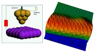
Caption: A scanning tunneling microscope determines the topography and orientation of the graphene nanoribbons on the atomic scale. In spectroscopy mode, it determines changes in the density of electronic states, from the nanoribbon's interior to its edge.
Credit: Crommie et al, Lawrence Berkeley National Laboratory. Usage Restrictions: with credit as given. | The team's research not only confirms theoretical predictions but opens the prospect of building quick-acting, energy-efficient nanoscale devices from graphene-nanoribbon switches, spin-valves, and detectors, based on either electron charge or electron spin. Farther down the road, graphene nanoribbon edge states open the possibility of devices with tunable giant magnetoresistance and other magnetic and optical effects.
Crommie and his colleagues have published their research in Nature Physics, available May 8, 2011 in advanced online publication.
The well-tempered nanoribbon
"Making flakes and sheets of graphene has become commonplace," Crommie says, "but until now, nanoribbons produced by different techniques have exhibited, at best, a high degree of inhomogeneity" – typically resulting in disordered ribbon structures with only short stretches of straight edges appearing at random. The essential first step in detecting nanoribbon edge states is access to uniform nanoribbons with straight edges, well-ordered on the atomic scale.
Hongjie Dai of Stanford University's Department of Chemistry and Laboratory for Advanced Materials, a member of the research team, solved this problem with a novel method of "unzipping" carbon nanotubes chemically. Graphene rolled into a cylinder makes a nanotube, and when nanotubes are unzipped in this way the slice runs straight down the length of the tube, leaving well-ordered, straight edges.
Graphene can be wrapped at almost any angle to make a nanotube. The way the nanotube is wrapped determines the pitch, or "chiral vector," of the nanoribbon edge when the tube is unzipped. A cut straight along the outer atoms of a row of hexagons produces a zigzag edge. A cut made at a 30-degree angle from a zigzag edge goes through the middle of the hexagons and yields scalloped edges, known as "armchair" edges. Between these two extremes are a variety of chiral vectors describing edges stepped on the nanoscale, in which, for example, after every few hexagons a zigzag segment is added at an angle.
These subtle differences in edge structure have been predicted to produce measurably different physical properties, which potentially could be exploited in new graphene applications. Steven Louie of UC Berkeley and Berkeley Lab's MSD was the research team's theorist; with the help of postdoc Oleg Yazyev, Louie calculated the expected outcomes, which were then tested against experiment.
Chenggang Tao of MSD and UCB led a team of graduate students in performing scanning tunneling microscopy (STM) of the nanoribbons on a gold substrate, which resolved the positions of individual atoms in the graphene nanoribbons. The team looked at more than 150 high-quality nanoribbons with different chiralities, all of which showed an unexpected feature, a regular raised border near their edges forming a hump or bevel. Once this was established as a real edge feature – not the artifact of a folded ribbon or a flattened nanotube – the chirality and electronic properties of well-ordered nanoribbon edges could be measured with confidence, and the edge regions theoretically modeled.
Electronics at the edge
"Two-dimensional graphene sheets are remarkable in how freely electrons move through them, including the fact that there's no band gap," Crommie says.
"Nanoribbons are different: electrons can become trapped in narrow channels along the nanoribbon edges. These edge-states are one-dimensional, but the electrons on one edge can still interact with the edge electrons on the other side, which causes an energy gap to open up."
Using an STM in spectroscopy mode (STS), the team measured electronic density changes as an STM tip was moved from a nanoribbon edge inward toward its interior. Nanoribbons of different widths were examined in this way. The researchers discovered that electrons are confined to the edge of the nanoribbons, and that these nanoribbon-edge electrons exhibit a pronounced splitting in their energy levels.
"In the quantum world, electrons can be described as waves in addition to being particles," Crommie notes. He says one way to picture how different edge states arise is to imagine an electron wave that fills the length of the ribbon and diffracts off the atoms near its edge. The diffraction patterns resemble water waves coming through slits in a barrier. |
For nanoribbons with an armchair edge, the diffraction pattern spans the full width of the nanoribbon; the resulting electron states are quantized in energy and extend spatially throughout the entire nanoribbon. For nanoribbons with a zigzag edge, however, the situation is different. Here diffraction from edge atoms leads to destructive interference, causing the electron states to localize near the nanoribbon edges. Their amplitude is greatly reduced in the interior.
The energy of the electron, the width of the nanoribbon, and the chirality of its edges all naturally affect the nature and strength of these nanoribbon electronic states, an indication of the many ways the electronic properties of nanoribbons can be tuned and modified.
Says Crommie, "The optimist says, 'Wow, look at all the ways we can control these states – this might allow a whole new technology!' The pessimist says, 'Uh-oh, look at all the things that can disturb a nanoribbon's behavior – how are we ever going to achieve reproducibility on the atomic scale?'"
Crommie himself declares that "meeting this challenge is a big reason for why we do research. Nanoribbons have the potential to form exciting new electronic, magnetic, and optical devices at the nanoscale. We might imagine photovoltaic applications, where absorbed light leads to useful charge separation at nanoribbon edges. We might also imagine spintronics applications, where using a side-gate geometry would allow control of the spin polarization of electrons at a nanoribbon's edge."
Although getting there won't be simple -- "The edges have to be controlled," Crommie emphasizes -- "what we've shown is that it's possible to make nanoribbons with good edges and that they do, indeed, have characteristic edge states similar to what theorists had expected. This opens a whole new area of future research involving the control and characterization of graphene edges in different nanoscale geometries."
###
Lawrence Berkeley National Laboratory addresses the world's most urgent scientific challenges by advancing sustainable energy, protecting human health, creating new materials, and revealing the origin and fate of the universe. Founded in 1931, Berkeley Lab's scientific expertise has been recognized with 12 Nobel prizes. The University of California manages Berkeley Lab for the U.S. Department of Energy's Office of Science. For more, visit
www.lbl.gov.
Contact: Paul Preuss
paul_preuss@lbl.gov 510-486-6249
DOE/Lawrence Berkeley National Laboratory


No comments:
Post a Comment