Tuesday, August 31, 2010

Unprecedented look at oxide interfaces reveals unexpected structures on atomic scale

OAK RIDGE, Tenn., — Thin layers of oxide materials and their interfaces have been observed in atomic resolution during growth for the first time by researchers at the Center for Nanophase Materials Sciences at the Department of Energy's Oak Ridge National Laboratory, providing new insight into the complicated link between their structure and properties.

"Imagine you suddenly had the ability to see in color, or in 3-D," said the CNMS's Sergei Kalinin. "That is how close we have been able to look at these very small interfaces."

The paper was published online in ACS Nano with ORNL's Junsoo Shin as lead author.

A component of magnetoelectronics and spintronics, oxide interfaces have the potential to replace silicon-based microelectronic devices and improve the power and memory retention of other electronic technologies.

oxide interfaces

A new scanning tunneling microscopy and low energy electron diffraction technique developed at Oak Ridge National Laboratory captured this 50 nm x 50 nm image of an oxide surface. Each bright dot is a single atom of material.
However, oxide interfaces are difficult to analyze at the atomic scale because once the oxides are removed from their growth chamber they become contaminated. To circumvent this problem, ORNL researchers led by Art Baddorf built a unique system that allows scanning tunneling microscopy and low energy electron diffraction to capture images of the top layer of the oxide while in situ, or still in the vacuum chamber where the materials were grown by powerful laser pulses.

Many studies of similar oxide interfaces utilize a look from the side, typically achieved by aberration corrected scanning transmission electron microscopy (STEM). The ORNL team has used these cross-sectional images to map the oxide organization.
However, like a sandwich, oxide interfaces may be more than what they appear from the side. In order to observe the interactive layer of the top and bottom oxide, the group has used scanning tunneling microscopy to get an atomically resolved view of the surface of the oxide, and observed its evolution during the growth of a second oxide film on top.

"Instead of seeing a perfectly flat, square lattice that scientists thought these interfaces were before, we found a different and very complicated atomic ordering," said Baddorf. "We really need to reassess what we know about these materials."

Oxides can be used in different combinations to produce unique results. For instance, isolated, two oxides may be insulators but together the interface may become conductive. By viewing the atomic structure of one oxide, scientists can more effectively couple oxides to perform optimally in advanced technological applications such as transistors.

Kalinin says the correct application of these interface-based materials may open new pathways for development of computer processors and energy storage and conversion devices, as well as understanding basic physics controlling these materials.

"In the last 10 years, there has been only limited progress in developing beyond-silicon information technologies," Kalinin said. "Silicon has limitations that have been reached, and this has motivated people to explore other options."

Atomic resolution of interface structures during oxide growth will better enable scientists to identify defects of certain popular oxide combinations and could help narrow selections of oxides to spur new or more efficient commercial applications.

This research is supported by the U.S. Department of Energy, Office of Science.

The Center for Nanophase Materials Sciences at ORNL is one of the five DOE Nanoscale Science Research Centers supported by the DOE Office of Science, premier national user facilities for interdisciplinary research at the nanoscale. Together the NSRCs comprise a suite of complementary facilities that provide researchers with state-of-the-art capabilities to fabricate, process, characterize and model nanoscale materials, and constitute the largest infrastructure investment of the National Nanotechnology Initiative. The NSRCs are located at DOE's Argonne, Brookhaven, Lawrence Berkeley, Oak Ridge and Sandia and Los Alamos national laboratories. For more information about the DOE NSRCs, please visit nano.energy.gov.

ORNL is managed by UT-Battelle for the Department of Energy's Office of Science.

Contact: Katie Freeman freemanke@ornl.gov 865-574-4160 DOE/Oak Ridge National Laboratory

Monday, August 30, 2010

NIST nanofluidic 'multi-tool' separates and sizes nanoparticles

A wrench or a screwdriver of a single size is useful for some jobs, but for a more complicated project, you need a set of tools of different sizes. Following this guiding principle, researchers at the National Institute of Standards and Technology (NIST) have engineered a nanoscale fluidic device that functions as a miniature "multi-tool" for working with nanoparticles—objects whose dimensions are measured in nanometers, or billionths of a meter.

First introduced in March 2009 (see "NIST-Cornell Team Builds World's First Nanofluidic Device with Complex 3-D Surfaces", the device consists of a chamber with a cascading "staircase" of 30 nanofluidic channels ranging in depth from about 80 nanometers at the top to about 620 nanometers (slightly smaller than an average bacterium) at the bottom. Each of the many "steps" of the staircase provides another "tool" of a different size to manipulate nanoparticles in a method that is similar to how a coin sorter separates nickels, dimes and quarters.

Nanofluidic Multi-Tool

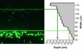
Caption: A 3-D nanofluidic "staircase" channel with many depths was used to separate and measure a mixture of different-sized fluorescent nanoparticles. Larger (brighter) and smaller (dimmer) particles were forced toward the shallow side of the channel (fluorescence micrograph on left). The particles stopped at the "steps" of the staircase with depths that matched their sizes.

Credit: S.M. Stavis, NIST. Usage Restrictions: None/
In a new article in the journal Lab on a Chip*, the NIST research team demonstrates that the device can successfully perform the first of a planned suite of nanoscale tasks—separating and measuring a mixture of spherical nanoparticles of different sizes (ranging from about 80 to 250 nanometers in diameter) dispersed in a solution. The researchers used electrophoresis—the method of moving charged particles through a solution by forcing them forward with an applied electric field—to drive the nanoparticles from the deep end of the chamber across the device into the progressively shallower channels. The nanoparticles were labeled with fluorescent dye so that their movements could be tracked with a microscope.
As expected, the larger particles stopped when they reached the steps of the staircase with depths that matched their diameters of around 220 nanometers. The smaller particles moved on until they, too, were restricted from moving into shallower channels at depths of around 110 nanometers. Because the particles were visible as fluorescent points of light, the position in the chamber where each individual particle was stopped could be mapped to the corresponding channel depth. This allowed the researchers to measure the distribution of nanoparticle sizes and validate the usefulness of the device as both a separation tool and reference material. Integrated into a microchip, the device could enable the sorting of complex nanoparticle mixtures, without observation, for subsequent application. This approach could prove to be faster and more economical than conventional methods of nanoparticle sample preparation and characterization.

The NIST team plans to engineer nanofluidic devices optimized for different nanoparticle sorting applications. These devices could be fabricated with tailored resolution (by increasing or decreasing the step size of the channels), over a particular range of particle sizes (by increasing or decreasing the maximum and minimum channel depths), and for select materials (by conforming the surface chemistry of the channels to optimize interaction with a specific substance). The researchers are also interested in determining if their technique could be used to separate mixtures of nanoparticles with similar sizes but different shapes—for example, mixtures of tubes and spheres. ###

* S.M. Stavis, J. Geist and M. Gaitan. Separation and metrology of nanoparticles by nanofluidic size exclusion. Lab on a Chip, forthcoming, August 2010.

Contact: Michael E. Newman michael.newman@nist.gov 301-975-3025 National Institute of Standards and Technology (NIST)

Sunday, August 29, 2010

New findings promising for 'transformation optics,' cloaking

WEST LAFAYETTE, Ind. -- Researchers have overcome a fundamental obstacle in using new "metamaterials" for radical advances in optical technologies, including ultra-powerful microscopes and computers and a possible invisibility cloak.

The metamaterials have been plagued by a major limitation: too much light is "lost," or absorbed by metals such as silver and gold contained in the metamaterials, making them impractical for optical devices.

However, a Purdue University team has solved this hurdle, culminating three years of research based at the Birck Nanotechnology Center at the university's Discovery Park.

"This finding is fundamental to the whole field of metamaterials," said Vladimir M. Shalaev, Purdue's Robert and Anne Burnett Professor of Electrical and Computer Engineering. "We showed that, in principle, it's feasible to conquer losses and develop these materials for many applications."

metamaterials

This illustration shows the structure of a new device created by Purdue researchers to overcome a fundamental obstacle in using new "metamaterials" for radical advances in optical technologies, including ultrapowerful microscopes and computers and a possible invisibility cloak. The material developed by the researchers is a perforated, fishnet-like film made of repeating layers of silver and aluminum oxide. The researchers etched away a portion of the aluminum oxide between silver layers and replaced it with a "gain medium" to amplify light. (Birck Nanotechnology Center, Purdue University)
Research findings are detailed in a paper appearing on Aug. 5 in the journal Nature.

The material developed by Purdue researchers is made of a fishnet-like film containing holes about 100 nanometers in diameter and repeating layers of silver and aluminum oxide. The researchers etched away a portion of the aluminum oxide between silver layers and replaced it with a "gain medium" formed by a colored dye that can amplify light.

Other researchers have applied various gain media to the top of the fishnet film, but that approach does not produce sufficient amplification to overcome losses, Shalaev said. Instead, the Purdue team found a way to place the dye between the two fishnet layers of silver, where the "local field" of light is far stronger than on the surface of the film, causing the gain medium to work 50 times more efficiently.
The approach was first developed by former Purdue doctoral student Hsiao-Kuan Yuan, now at Intel Corp., and it was further developed and applied by doctoral student Shumin Xiao.

Unlike natural materials, metamaterials are able to reduce the "index of refraction" to less than one or less than zero. Refraction occurs as electromagnetic waves, including light, bend when passing from one material into another. It causes the bent-stick-in-water effect, which occurs when a stick placed in a glass of water appears bent when viewed from the outside.

Being able to create materials with an index of refraction that's negative or between one and zero promises a range of potential breakthroughs in a new field called transformation optics. Possible applications include a "planar hyperlens" that could make optical microscopes 10 times more powerful and able to see objects as small as DNA; advanced sensors; new types of "light concentrators" for more efficient solar collectors; computers and consumer electronics that use light instead of electronic signals to process information; and a cloak of invisibility.

Excitement about metamaterials has been tempered by the fact that too much light is absorbed by the materials. However, the new approach can dramatically reduce the "absorption coefficient," or how much light and energy is lost, and might amplify the incident light so that the metamaterial becomes "active," Shalaev said.

"What's really important is that the absorption coefficient can be as small as only one-millionth of what it was before using our approach," Shalaev said. "We can even have amplification of light instead of its absorption. Here, for the first time, we showed that metamaterials can have a negative refractive index and amplify light."

The Nature paper was written by Xiao, senior research scientist Vladimir P. Drachev, principal research scientist Alexander V. Kildishev, doctoral student Xingjie Ni, postdoctoral fellow Uday K. Chettiar, Yuan, and Shalaev.

Fabricating the material was a major challenge, Shalaev said.

First, the researchers had to learn how to precisely remove as much as possible of the aluminum oxide layer in order to vacate space for dye without causing a collapse of the structure.

"You remove it almost completely but leave a little bit to act as pillars to support the structure, and then you spin coat the dye-doped polymer inside the structure," he said.

The researchers also had to devise a way to deposit just the right amount of dye mixed with an epoxy between the silver layers of the perforated film.

"You can't deposit too much dye and epoxy, which have a positive refractive index, but only a thin layer about 50 nanometers thick, or you lose the negative refraction," Shalaev said.

Future work may involve creating a technology that uses an electrical source instead of a light source, like semiconductor lasers now in use, which would make them more practical for computer and electronics applications. ###

The work was funded by the U.S. Army Research Office and the National Science Foundation.

Writer: Emil Venere, (765) 494-4709, venere@purdue.edu

Source: Vladimir Shalaev, (765) 494-9855, shalaev@ecn.purdue.edu

Related Web site: Vladimir Shalaev, cobweb.ecn.purdue.edu/~shalaev/

Note to Journalists: Journalists may obtain a copy of the research paper by contacting Nature at press@nature.com or calling (212) 726-9231.

Saturday, August 28, 2010

Pitt-led researchers to build foundation for quantum supercomputers with $7.5 million federal grant

Team led by Pitt physics and astronomy professor Jeremy Levy to resolve the major challenges to creating computers more powerful and efficient than all the world's existing computers with five-year US Department of Defense MURI award.

PITTSBURGH—A research team based at the University of Pittsburgh has received a five-year, $7.5 million grant from the U.S. Department of Defense to tackle some of the most significant challenges preventing the development of quantum computers, powerful devices that could solve problems too complex for all of the world's computers working together over the age of the Universe to crack. The project was one of 32 nationwide selected from 152 proposals to receive a grant from the Multi-University Research Initiative (MURI) program; a total of $227 million was distributed to institutions that include Harvard University, the Massachusetts Institute of Technology, the University of Illinois at Urbana-Champaign, and the University of Pennsylvania.

Jeremy Levy, University of Pittsburgh

Caption: This is Pitt physics and astronomy professor Jeremy Levy.

Credit: University of Pittsburgh. Usage Restrictions: None.
Jeremy Levy, a professor of physics and astronomy in Pitt's School of Arts and Sciences, will lead a team of researchers from Cornell University, Stanford University, the University of California at Santa Barbara, the University of Michigan, and the University of Wisconsin in combining the properties of semiconductors—such as those used to make computer processors, and superconductors—which allow for the perfect flow of electricity, into a single material suitable for the development of quantum computers. The team will use these superconducting semiconductors to develop new types of quantum memory, perform quantum simulation, and create new methods for transferring quantum information from one medium to another.
These functions are essential to realizing quantum computers—which are yet to exist in any practical form—but require a precise control of the laws of quantum physics that has so far been difficult to achieve, Levy explained.

One of the most significant challenges with any approach to quantum computation is the inevitable loss of information. Group member Chetan Nayak, a physics professor at UC-Santa Barbara, has theorized that very thin sheets of certain types of superconductors have topological quantum excitations that can be used to make quantum memories highly immune to errors. The development of materials that can support these excitations will be undertaken by Chang-Beom Eom, a professor of materials science and engineering at Wisconsin; Harold Hwang, a professor of applied physics at Stanford; and Darrell Schlom, an engineering professor at Cornell. Xiaoqing Pan, a University of Michigan professor of materials science and engineering, will perform atomic-scale characterization of these structures.

A second research goal involves using superconducting semiconductors to perform quantum simulations of physical systems. To do this, the team will use a technique Levy developed that allows for atomic-scale devices such as transistors and computer processors to be created and erased on a single platform that functions like a microscopic Etch A SketchTM, the drawing toy that inspired Levy's idea; Levy reported on the platform in the Feb. 20, 2009, edition of Science. For the MURI project, Levy will create a new near-atomic scale lattice that will be used to experiment with new materials and search for superconducting phenomena.

The project's third thrust involves the transfer of quantum information from one physical system to another. Quantum bits are efficiently stored in nanoscale defects found in diamonds. David Awschalom, a professor of physics and electrical engineering at UC-Santa Barbara, will develop ways of transferring quantum information between these diamond defects and superconducting microwave resonators. ###

The MURI program is overseen by the U.S. Army Research Office, the U.S. Office of Naval Research, and the U.S. Air Force Office of Scientific Research. It is intended to support research across multiple academic institutions and departments in order to accelerate research and the transition of research results to application. More information on the 2010 MURI grants is available on the Department of Defense Web site at www.defense.gov/releases/.

Contact: Morgan Kelly mekelly@pitt.edu 412-624-4356 University of Pittsburgh

Thursday, August 26, 2010

Iron oxide nanoparticles becoming tools for brain tumor imaging and treatment

Tiny particles of iron oxide could become tools for simultaneous tumor imaging and treatment, because of their magnetic properties and toxic effects against brain cancer cells. In mice, researchers from Emory University School of Medicine have demonstrated how these particles can deliver antibodies to implanted brain tumors, while enhancing tumor visibility via magnetic resonance imaging (MRI).

The results are published online by the journal Cancer Research.

The lead author is Costas Hadjipanayis, assistant professor of neurosurgery at Emory University School of Medicine, director of Emory's Brain Tumor Nanotechnology Laboratory, and chief of neurosurgery service at Emory University Hospital Midtown.

Glioblastoma multiforme (GBM), the most common and most aggressive primary brain tumor, often comes back because cancer cells infiltrate into the surrounding brain tissue and survive initial treatment.

Brain Tumor with Nanoparticles

Caption: Iron oxide nanoparticles “darken” the MRI signal of a brain tumor implanted into a mouse.

Credit: Costas Hadjipanayis. Usage Restrictions: None.

Iron Oxide Nanoparticle

Caption: This is a schematic of an iron oxide nanoparticle.

Credit: Costas Hadjipanayis. Usage Restrictions: None.
Hadjipanayis' team designed tiny iron oxide particles (10 nanometers across), coated with a polymer and bioconjugated or linked to antibodies directed against a molecule that appears on the surface of glioblastoma cells.

This molecule, a shortened and continuously active form of the epidermal growth factor receptor (EGFRvIII), drives glioblastoma cell growth and accounts for radiation and chemotherapy resistance. EGFRvIII appears in about a third of glioblastomas and is only present on tumor cells and not the normal surrounding cells in the brain.

The team showed that the particles bind to and kill human glioblastoma cells, yet do not cause any toxicity to normal human astrocytes, which comprise the majority of cells in the brain. They used a technique called convection-enhanced delivery (CED) – continuous infusion of fluid under positive pressure – to introduce the iron oxide particles into mice that had human glioblastoma cells implanted intracranially.

The antibody-linked particles lengthened survival of the tumor-implanted mice: their median survival was 19 days compared to 16 days for bare particles and 11 days for no particles. The particles also made the tumor visible via MRI, darkening the area of the brain where the tumor is (see accompanying image).
Hui Mao, PhD associate professor of radiology, and his team of researchers, contributed MRI experiments showing the sensitive imaging qualities of the iron-oxide nanoparticles in vitro and in the mouse brain.

To heighten anti-cancer effects, the Brain Tumor Nanotechnology Laboratory is investigating the use of safe alternating magnetic fields for the generation of local hyperthermia (heating) against malignant brain tumors by magnetic nanoparticles.

Hadjipanayis and his team plan to translate the use of bioconjugated iron-oxide nanoparticles for use in canine brain tumor models at the University of Georgia College of Veterinary Medicine and into a human clinical trial for patients suffering from brain cancer. ###

The research was supported by the National Institutes of Health, EmTech Bio Inc., Southeastern Brain Tumor Foundation, the Georgia Cancer Coalition and the Dana Foundation.

Reference: C.G. Hadjipanayis, R. Machaidze, M. Kaluzova, L. Wang, A.J. Schuette, H. Chen, X. Wu and H. Mao. EGFRvIII antibody-conjugated iron oxide nanoparticles for magnetic resonance imaging-guided convection-enhanced deliver and targeted therapy of glioblastoma. Cancer Res. 70: 6303-12 (August 1, 2010)

Writer: Quinn Eastman

For more information about Emory's Woodruff Health Sciences Center, see emoryhealthsciences.org

Contact: Janet Christenbury jmchris@emory.edu 404-727-8599 Emory University

Wednesday, August 25, 2010

New catalyst of platinum nanoparticles could lead to conk-out free, stable fuel cells

ITHACA, N.Y. — In the quest for efficient, cost-effective and commercially viable fuel cells, scientists at Cornell University's Energy Materials Center have discovered a catalyst and catalyst-support combination that could make fuel cells more stable, conk-out free, inexpensive and more resistant to carbon monoxide poisoning. (Journal of the American Chemical Society, July 12, 2010.)

The research, "Highly Stable and CO-Tolerant Pt/Ti0.7W0.3O2 Electrocatalyst for Proton-Exchange Membrane Fuel Cells," led by Héctor D. Abruña, Cornell professor of Chemistry and Chemical Biology and director of the Energy Materials Center at Cornell (emc2); Francis J. DiSalvo, Cornell professor Chemistry and Chemical Biology; Deli Wang, post doctoral researcher; Chinmayee V. Subban, graduate student; Hongsen Wang, research associate; and Eric Rus, graduate student. Hydrogen fuel cells offer an appealing alternative to gasoline-burning cars: They have the potential to power vehicles for long distances using hydrogen as fuel, mitigate carbon dioxide production and emit only water vapor.

New catalyst of platinum nanoparticles

Fuel cells work by electrochemically decomposing fuel instead of burning it, converting energy directly into electricity.
However, fuel cells generally require very pure hydrogen to work. That means that conventional fuels must be stripped of carbon monoxide – a process that is too expensive to make fuel cells commercially viable.

Fuel cells work by electrochemically decomposing fuel instead of burning it, converting energy directly into electricity.

The problem is that platinum and platinum/ruthenium alloys, which are often used as catalysts in PEM (proton exchange membrane) fuel cells, are expensive and easily rendered ineffective by exposure to even low levels of carbon monoxide.
To create a catalyst system that can tolerate more carbon monoxide, Abruña, DiSalvo and colleagues deposited platinum nanoparticles on a support material of titanium oxide with added tungsten to increase its electrical conductivity. Their research shows that the new material works with fuel that contains as much as 2 percent carbon monoxide – a level that is about 2000 times that which typically poisons pure platinum. Also, the material is more stable and less expensive than pure platinum. With the new catalyst, said Abruña, "you can use much less-clean hydrogen, and that's more cost-effective because hydrogen derived from petroleum has a very high content of carbon monoxide. You need to scrub off the carbon monoxide and it's very expensive to do that."

The researchers are now preparing to put the catalyst to the test in real fuel cells. "So far, indications are very good," Abruña said. In preliminary experiments comparing the new material's performance with pure platinum, he added, the platinum cell was readily poisoned by carbon monoxide and conked out early. Said Abruña: "But ours was still running like a champ." ###

The research was supported by the U.S. Department of Energy and by the Energy Materials Center at Cornell, an Energy Frontier Research Center funded by the Department of Energy.

Contact: Blaine Friedlander bpf2@cornell.edu 607-254-8093 Cornell University

Tuesday, August 24, 2010

Nano 'pin art': NIST arrays are step toward mass production of nanowires

NIST researchers grow nanowires made of semiconductors—gallium nitride alloys—by depositing atoms layer-by-layer on a silicon crystal under high vacuum. NIST has the unusual capability to produce these nanowires without using metal catalysts, thereby enhancing luminescence and reducing defects. NIST nanowires also have excellent mechanical quality factors.

The latest experiments, described in Advanced Functional Materials,* maintained the purity and defect-free crystal structure of NIST nanowires while controlling diameter and placement better than has been reported by other groups for catalyst-based nanowires. Precise control of diameter and placement is essential before nanowires can be widely used.

The key trick in the NIST technique is to grow the wires through precisely defined holes in a stencil-like mask covering the silicon wafer.

semiconductor nanowires

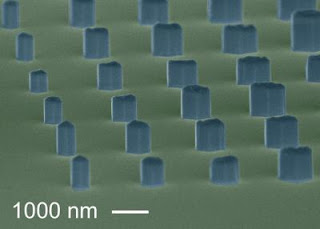
Caption: This is a colorized micrograph of semiconductor nanowires grown at NIST in a precisely controlled array of sizes and locations.

Credit: K. Bertness, NIST. Usage Restrictions: None.
The NIST nanowires were grown through openings in patterned silicon nitride masks. About 30,000 nanowires were grown per 76-millimeter-wide wafer. The technique controlled nanowire location almost perfectly. Wires grew uniformly through most openings and were absent on most of the mask surface.

Mask openings ranged from 300 to 1000 nanometers (nm) wide, in increments of 100 nm. In each opening of 300 nm or 400 nm, a single nanowire grew, with a well-formed hexagonal shape and a symmetrical tip with six facets. Larger openings produced more variable results. Openings of 400 nm to 900 nm yielded single-crystal nanowires with multifaceted tops.
Structures grown in 1,000-nm openings appeared to be multiple wires stuck together. All nanowires grew to about 1,000 nm tall over three days.

NIST researchers analyzed micrographs to verify the uniformity of nanowire shape and size statistically. The analysis revealed nearly uniform areas of wires of the same diameter as well as nearly perfect hexagonal shapes.

Growing nanowires on silicon is one approach NIST researchers are exploring for making "nanowires on a chip" devices. Although the growth temperatures are too high—over 800 degrees Celsius—for silicon circuitry to tolerate, there may be ways to grow the nanowires first and then protect them during circuitry fabrication, lead author Kris Bertness says. The research was partially supported by the Defense Advanced Research Projects Agency (DARPA) Center on NanoscaleScience and Technology for Integrated Micro/Nano-Electromechanical Transducers (iMINT) at the University of Colorado at Boulder. ###

* K. A. Bertness, A. W. Sanders, D. M. Rourke, T. E. Harvey, A. Roshko, J.B. Schlager and N. A. Sanford. Controlled nucleation of GaN nanowires grown with molecular beam epitaxy. Advanced Functional Materials. Published online: July 13, 2010. DOI: 10.1002/adfm.201000381

Contact: Laura Ost laura.ost@nist.gov 303-497-4880 National Institute of Standards and Technology (NIST)

Monday, August 23, 2010

One more step on the path to quantum computers

Ultra-strong interaction between light and matter realized.

The interaction between matter and light represents one of the most fundamental processes in physics. Whether a car that heats up like an oven in the summer due to the absorption of light quanta or solar cells that extract electricity from light or light-emitting diodes that convert electricity into light, we encounter the effects of these processes throughout our daily lives. Understanding the interactions between individual light particles – photons – and atoms is crucial for the development of a quantum computer.

Physicists from the Technische Universitaet Muenchen (TUM), the Walther-Meissner-Institute for Low Temperature Research of the Bavarian Academy of Sciences (WMI) and the Augsburg University have now, in collaboration with partners from Spain, realized an ultrastrong interaction between microwave photons and the atoms of a nano-structured circuit.

Interaction Between a Superconducting Electrical Circuit and a Microwave Photon

Caption: This is an impression of the interaction between a superconducting electrical circuit and a microwave photon.

Credit: Dr. A. Marx, Technische Universitaet Muenchen. Usage Restrictions: None.

Superconducting Circuit for Ultrastrong Interactions between Light and Artificial Atoms

Caption: This is an electron microscopical picture of the superconducting circuit (red: Aluminum-Qubit, grey: Niob-Resonator, green: Silicon substrate).

Credit: Thomasz Niemczyk, Technische Universitaet Muenchen. Usage Restrictions: None.
The realized interaction is ten times stronger than levels previously achieved for such systems.

The simplest system for investigating the interactions between light and matter is a so-called cavity resonator with exactly one light particle and one atom captured inside (cavity quantum electrodynamics, cavity QED). Yet since the interaction is very weak, these experiments are very elaborate. A much stronger interaction can be obtained with nano-structured circuits in which metals like aluminum become superconducting at temperatures just above absolute zero (circuit QED). Properly configured, the billions of atoms in the merely nanometer thick conductors behave like a single artificial atom and obey the laws of quantum mechanics. In the simplest case, one obtains a system with two energy states, a so-called quantum bit or qubit.

Coupling these kinds of systems with microwave resonators has opened a rapidly growing new research domain in which the TUM Physics, the WMI and the cluster of excellence Nanosystems Initiative Munich (NIM) are leading the field. In contrast to cavity QED systems, the researchers can custom tailor the circuitry in many areas.
To facilitate the measurements, Professor Gross and his team captured the photon in a special box, a resonator. This consists of a superconducting niobium conducting path that is configured with strongly reflective "mirrors" for microwaves at both ends. In this resonator, the artificial atom made of an aluminum circuit is positioned so that it can optimally interact with the photon. The researchers achieved the ultrastrong interactions by adding another superconducting component into their circuit, a so-called Josephson junction.

The measured interaction strength was up to twelve percent of the resonator frequency. This makes it ten times stronger than the effects previously measureable in circuit QED systems and thousands of times stronger than in a true cavity resonator. However, along with their success the researchers also created a new problem: Up to now, the Jaynes-Cummings theory developed in 1963 was able to describe all observed effects very well. Yet, it does not seem to apply to the domain of ultrastrong interactions. "The spectra look like those of a completely new kind of object," says Professor Gross. "The coupling is so strong that the atom-photon pairs must be viewed as a new unit, a kind of molecule comprising one atom and one photon.

Experimental and theoretical physicists will need some time to examine this more closely. However, the new experimental inroads into this domain are already providing researchers with a whole array of new experimental options. The targeted manipulation of such atom-photon pairs could hold the key to quanta-based information processing, the so-called quantum computers that would be vastly superior to today's computers. ###

The research was funded by the Deutsche Forschungsgemeinschaft (DFG) (Cluster of Excellence Nanosystems Initiative Munich and SFB 631), the European Community (EuroSQIP, SOLID), as well as the Spanish Ministry for Science and Innovation.

Contact: Dr. Andreas Battenberg battenberg@zv.tum.de 49-892-891-0510 Technische Universitaet Muenchen

Sunday, August 22, 2010

Decontaminating dangerous drywall VIDEO

Nanomaterial in novel home-air treatment counters hazards from toxic drywall.

A nanomaterial originally developed to fight toxic waste is now helping reduce debilitating fumes in homes with corrosive drywall.

Developed by Kenneth Klabunde of Kansas State University, and improved over three decades with support from the National Science Foundation, the FAST-ACT material has been a tool of first responders since 2003.

Now, NanoScale Corporation of Manhattan, Kansas--the company Klabunde co-founded to market the technology--has incorporated FAST-ACT into a cartridge that breaks down the corrosive drywall chemicals.

Homeowners have reported that the chemicals--particularly sulfur compounds such as hydrogen sulfide and sulfur dioxide--have caused respiratory illnesses, wiring corrosion and pipe damage in thousands of U.S. homes with sulfur-rich, imported drywall.


This video shows how the FAST-ACT powders work, how they are made and how they are used in situations ranging from chemical spills to gas releases in enclosed chambers.

Credit: Cliff Braverman and Trent Schindler, NSF; NanoScale Materials, Inc.; Kansas State University

"It is devastating to see what has happened to so many homeowners because of the corrosive drywall problem, but I am glad the technology is available to help," said Klabunde. "We've now adapted the technology we developed through years of research for FAST-ACT for new uses by homeowners, contractors and remediators."

The new cartridge, called OdorKlenz®, takes the place of the existing air filter in a home. The technology is similar to one that NanoScale adapted in 2008 for use by a major national disaster restoration service company for odors caused by fire and water damage.

In homes with corrosive drywall, the cartridge is used in combination with related FAST-ACT-based, OdorKlenz® surface treatments (and even laundry additives) to remove the sulfur-bearing compounds causing the corrosion issues.

Developers at NanoScale tested their new air cartridge in affected homes that were awaiting drywall removal, and in every case, odor dropped to nearly imperceptible levels within 10 days or less and corrosion was reduced.

The FAST-ACT material is a non-toxic mineral powder composed of the common elements magnesium, titanium and oxygen. While metal oxides similar to FAST-ACT have an established history tackling dangerous compounds, none have been as effective.

NanoScale's breakthrough was a new method to manufacture the compound as a nanocrystalline powder with extremely high surface area--only a few tablespoons have as much surface area as a football field.

The surface area allows more interactions between the metal oxides and the toxic molecules, enabling the powder to capture and destroy a large quantity of hazardous chemicals ranging from sulfuric acid to VX gas--and their hazardous byproducts--in minutes.

"The concept of nano-sized adsorbents as both a cost-efficient, useful product for first responders and an effective product for in-home use illustrates the wide spectrum of possibilities for this technology," said NSF program director Rosemarie Wesson, who oversaw NanoScale's NSF Small Business Innovation Resarch grants. "It is great to see the original work we supported to help reduce the toxic effects of hazardous spills now expand into other applications."

In coming months, the company is proposing its technology for use in Gulf Coast residences affected by the recent oil spill and other hazardous situations where airborne toxins are causing harm. ###

In addition to extensive support from NSF, the development of FAST ACT and NanoScale's technology has been supported by grants from the U.S. Army, DTRA, Air Force, DARPA, JPEO, MARCORSYSCOM , the CTTSO, USSOCOM, NIOSH, DOE, NIH and EPA.

Contact: Joshua A. Chamot jchamot@nsf.gov 703-292-7730 National Science Foundation

Media Contacts: Joshua A. Chamot, NSF (703) 292-7730 jchamot@nsf.gov Kyle Knappenberger, NanoScale Corporation (785) 537-0179 KKnappenberger@nanoscalecorporation.com

Principal Investigators: Kenneth Klabunde, Kansas State University (785) 532-6849 kenjk@ksu.edu

Saturday, August 21, 2010

Graphene under strain creates gigantic pseudo-magnetic fields

Graphene, the extraordinary form of carbon that consists of a single layer of carbon atoms, has produced another in a long list of experimental surprises. In the current issue of the journal Science, a multi-institutional team of researchers headed by Michael Crommie, a faculty senior scientist in the Materials Sciences Division at the U.S. Department of Energy's Lawrence Berkeley National Laboratory and a professor of physics at the University of California at Berkeley, reports the creation of pseudo-magnetic fields far stronger than the strongest magnetic fields ever sustained in a laboratory – just by putting the right kind of strain onto a patch of graphene.

"We have shown experimentally that when graphene is stretched to form nanobubbles on a platinum substrate, electrons behave as if they were subject to magnetic fields in excess of 300 tesla, even though no magnetic field has actually been applied," says Crommie. "This is a completely new physical effect that has no counterpart in any other condensed matter system."

Graphene Bubble

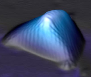
Caption: In this scanning tunneling microscopy image of a graphene nanobubble, the hexagonal two-dimensional graphene crystal is seen distorted and stretched along three main axes. The strain creates pseudo-magnetic fields far stronger than any magnetic field ever produced in the laboratory

Credit: courtesy of Micheal Crommie, Berkeley Lab. Usage Restrictions: None.

Graphene Bubbles

Caption: A patch of graphene at the surface of a platinum substrate exhibits four triangular nanobubbles at its edges and one in the interior. Scanning tunneling spectroscopy taken at intervals across one nanobubble (inset) shows local electron densities clustering in peaks at discrete Landau-level energies. Pseudo-magnetic fields are strongest at regions of greatest curvature.

Credit: courtesy of Michael Crommie, Berkeley Lab. Usage Restrictions: None.
Crommie notes that "for over 100 years people have been sticking materials into magnetic fields to see how the electrons behave, but it's impossible to sustain tremendously strong magnetic fields in a laboratory setting." The current record is 85 tesla for a field that lasts only thousandths of a second. When stronger fields are created, the magnets blow themselves apart.

The ability to make electrons behave as if they were in magnetic fields of 300 tesla or more – just by stretching graphene – offers a new window on a source of important applications and fundamental scientific discoveries going back over a century. This is made possible by graphene's electronic behavior, which is unlike any other material's.

A carbon atom has four valence electrons; in graphene (and in graphite, a stack of graphene layers), three electrons bond in a plane with their neighbors to form a strong hexagonal pattern, like chicken-wire. The fourth electron sticks up out of the plane and is free to hop from one atom to the next. The latter pi-bond electrons act as if they have no mass at all, like photons. They can move at almost one percent of the speed of light.

The idea that a deformation of graphene might lead to the appearance of a pseudo-magnetic field first arose even before graphene sheets had been isolated, in the context of carbon nanotubes (which are simply rolled-up graphene). In early 2010, theorist Francisco Guinea of the Institute of Materials Science of Madrid and his colleagues developed these ideas and predicted that if graphene could be stretched along its three main crystallographic directions, it would effectively act as though it were placed in a uniform magnetic field. This is because strain changes the bond lengths between atoms and affects the way electrons move between them. The pseudo-magnetic field would reveal itself through its effects on electron orbits.
In classical physics, electrons in a magnetic field travel in circles called cyclotron orbits. These were named following Ernest Lawrence's invention of the cyclotron, because cyclotrons continuously accelerate charged particles (protons, in Lawrence's case) in a curving path induced by a strong field.

Viewed quantum mechanically, however, cyclotron orbits become quantized and exhibit discrete energy levels. Called Landau levels, these correspond to energies where constructive interference occurs in an orbiting electron's quantum wave function. The number of electrons occupying each Landau level depends on the strength of the field – the stronger the field, the more energy spacing between Landau levels, and the denser the electron states become at each level – which is a key feature of the predicted pseudo-magnetic fields in graphene.

Describing their experimental discovery, Crommie says, "We had the benefit of a remarkable stroke of serendipity."

Crommie's research group had been using a scanning tunneling microscope to study graphene monolayers grown on a platinum substrate. A scanning tunneling microscope works by using a sharp needle probe that skims along the surface of a material to measure minute changes in electrical current, revealing the density of electron states at each point in the scan while building an image of the surface.

Crommie was meeting with a visiting theorist from Boston University, Antonio Castro Neto, about a completely different topic when a group member came into his office with the latest data.

"It showed nanobubbles, little pyramid-like protrusions, in a patch of graphene on the platinum surface," Crommie says, "and associated with the graphene nanobubbles there were distinct peaks in the density of electron states."

Crommie says his visitor, Castro Neto, took one look and said, "That looks like the Landau levels predicted for strained graphene."

Sure enough, close examination of the triangular bubbles revealed that their chicken-wire lattice had been stretched precisely along the three axes needed to induce the strain orientation that Guinea and his coworkers had predicted would give rise to pseudo-magnetic fields. The greater the curvature of the bubbles, the greater the strain, and the greater the strength of the pseudo-magnetic field. The increased density of electron states revealed by scanning tunneling spectroscopy corresponded to Landau levels, in some cases indicating giant pseudo-magnetic fields of 300 tesla or more.

"Getting the right strain resulted from a combination of factors," Crommie says. "To grow graphene on the platinum we had exposed the platinum to ethylene" – a simple compound of carbon and hydrogen – "and at high temperature the carbon atoms formed a sheet of graphene whose orientation was determined by the platinum's lattice structure."

To get the highest resolution from the scanning tunneling microscope, the system was then cooled to a few degrees above absolute zero. Both the graphene and the platinum contracted – but the platinum shrank more, with the result that excess graphene pushed up into bubbles, measuring four to 10 nanometers (billionths of a meter) across and from a third to more than two nanometers high.

To confirm that the experimental observations were consistent with theoretical predictions, Castro Neto worked with Guinea to model a nanobubble typical of those found by the Crommie group. The resulting theoretical picture was a near-match to what the experimenters had observed: a strain-induced pseudo-magnetic field some 200 to 400 tesla strong in the regions of greatest strain, for nanobubbles of the correct size.

"Controlling where electrons live and how they move is an essential feature of all electronic devices," says Crommie. "New types of control allow us to create new devices, and so our demonstration of strain engineering in graphene provides an entirely new way for mechanically controlling electronic structure in graphene. The effect is so strong that we could do it at room temperature."

The opportunities for basic science with strain engineering are also huge. For example, in strong pseudo-magnetic fields electrons orbit in tight circles that bump up against one another, potentially leading to novel electron-electron interactions. Says Crommie, "this is the kind of physics that physicists love to explore." ###

"Strain-induced pseudo-magnetic fields greater than 300 tesla in graphene nanobubbles," by Niv Levy, Sarah Burke, Kacey Meaker, Melissa Panlasigui, Alex Zettl, Francisco Guinea, Antonio Castro Neto, and Michael Crommie, appears in the July 30 issue of Science. The work was supported by the Department of Energy's Office of Science and by the Office of Naval Research.

Lawrence Berkeley National Laboratory provides solutions to the world's most urgent scientific challenges including clean energy, climate change, human health, novel materials, and a better understanding of matter and force in the universe. It is a world leader in improving our lives and knowledge of the world around us through innovative science, advanced computing, and technology that makes a difference. Berkeley Lab is a U.S. Department of Energy (DOE) national laboratory managed by the University of California for the DOE Office of Science. Visit our website.

Contact: Paul Preuss paul_preuss@lbl.gov 510-486-6249 DOE/Lawrence Berkeley National Laboratory
Thursday, August 19, 2010

Behind the secrets of silk lie high-tech opportunities

A decade of research yields new uses for ancient material.

MEDFORD/SOMERVILLE, Mass. -- Tougher than a bullet-proof vest yet synonymous with beauty and luxury, silk fibers are a masterpiece of nature whose remarkable properties have yet to be fully replicated in the laboratory.

Thanks to their amazing mechanical properties as well as their looks, silk fibers have been important materials in textiles, medical sutures, and even armor for 5,000 years.

Silk spun by spiders and silk worms combines high strength and extensibility. This one-two punch is unmatched by synthetics, even though silk is made from a relatively simple protein processed from water.


Caption: Tougher than a bullet-proof vest yet synonymous with beauty and luxury, silks spun by worms and spiders are a masterpiece of nature whose properties have yet to be fully replicated in the laboratory. But Tufts University biomedical engineers report that success in unraveling the secrets of silk is taking silk from the world of textiles to technology. This silk card shows diffractive optics entirely constituted by pure silk obtained by pouring silk solution on nanopatterned molds and letting the solution dry and crystallize. The resulting film retains the pattern and is a free-standing optical component so flexible it can be rolled up.

Credit: Fiorenzo Omenetto/Tufts University. Usage Restrictions: Use only with appropriate caption and credit to Fiorenzo Omenetto/Tufts University.
But in recent years scientists have begun to unravel the secrets of silk.

In the July 30, 2010, issue of the journal Science, Tufts biomedical engineering researchers Fiorenzo Omenetto, Ph.D., and David Kaplan, Ph.D., report that "Silk-based materials have been transformed in just the past decade from the commodity textile world to a growing web of applications in more high technology directions."

Fundamental discoveries into how silk fibers are made have shown that chemistry, molecular biology and biophysics all play a role in the process. These discoveries have provided the basis for a new generation of applications for silk materials, from medical devices and drug delivery to electronics.

Edible Optics, Implantable Electronics

The Science paper notes that the development of silk hydrogels, films, fibers and sponges is making possible advances in photonics and optics, nanotechnology, electronics, adhesives and microfluidics, as well as engineering of bone and ligaments.
Because silk fiber formation does not rely on complex or toxic chemistries, such materials are biologically and environmentally friendly, even able to integrate with living systems.

Down the silk road of the future, Kaplan and Omenetto believe applications could include degradable and flexible electronic displays for sensors that are biologically and environmentally compatible and implantable optical systems for diagnosis and treatment. Progress in "edible optics" and implantable electronics has already been demonstrated by Kaplan and Omenetto, John Rogers at the University of Illinois at Urbana-Champaign, and others.

Many challenges remain. Kaplan and Omenetto say that key questions include how to fully replicate native silk assembly in the lab, how best to mimic silk protein sequences via genetic engineering to scale-up materials production, and how to use silk as a model polymer to spur new synthetic polymer designs that mimic natural silk's green chemistry.

Techniques for reprocessing natural silk protein in the lab continue to advance. Silks are also being cloned and expressed in a variety of hosts, including E. coli bacteria, fungi, plants and mammals, and through transgenic silkworms.

One day, efficient transgenic plants could be used to crop silk in much the same way that cotton is harvested today, the Tufts researchers note in their paper. In some regions, silk production might create a new microeconomy, as demand grows and production techniques improve.

"Based on the recent and rapid progression of silk materials from the ancient textile use into a host of new high-technology applications, we anticipate growth in the use of silks in a wide platform of applications will continue as answers to these remaining questions are obtained," say Omenetto and Kaplan. ###

Kaplan is chair of the Biomedical Engineering Department at Tufts School of Engineering and the Stern Family Professor in Engineering. He also directs the NIH Tissue Engineering Resource Center that involves Tufts and Columbia University. His work lies at the interface between biology and materials science and engineering, and he has been studying novel biomaterials, many of them silk-based, for 30 years. Professor of Biomedical Engineering Fiorenzo Omenetto is a frequent collaborator with Kaplan who has pioneered silk optics and use of silk as a green material for photonics and other high tech applications.

Support for this research on silk comes from the National Institutes of Health, National Science Foundation, Air Force Office of Science Research and the Defense Advanced Research Projects Agency.

Tufts University School of Engineering is uniquely positioned to educate the technological leaders of tomorrow. Located on Tufts' Medford/Somerville campus, the School of Engineering offers the best of a liberal arts college atmosphere coupled with the intellectual and technological resources of a world-class research-intensive university. Its goals are to educate engineers who are committed to the innovative and ethical application of technology to solve societal problems, and to be a leader among peer institutions in targeted areas of interdisciplinary research and education. Strategic areas of emphasis include programs in bioengineering, sustainability and innovation in engineering education.

Tufts University, located on three Massachusetts campuses in Boston, Medford/Somerville, and Grafton, and in Talloires, France, is recognized among the premier research universities in the United States. Tufts enjoys a global reputation for academic excellence and for the preparation of students as leaders in a wide range of professions. A growing number of innovative teaching and research initiatives span all Tufts campuses, and collaboration among the faculty and students in the undergraduate, graduate and professional programs across the university's schools is widely encouraged.

Contact: Kim Thurler kim.thurler@tufts.edu 617-627-3175 Tufts University

Wednesday, August 18, 2010

Graphene exhibits bizarre new behavior well suited to electronic devices

Subjected to a 3-point stretch, graphene develops bubbles of quantized electrons.

Graphene, a sheet of pure carbon heralded as a possible replacement for silicon-based semiconductors, has been found to have a unique and amazing property that could make it even more suitable for future electronic devices.

Physicists at the University of California, Berkeley, and the Lawrence Berkeley National Laboratory (LBNL) have found that when graphene is stretched in a specific way it sprouts nanobubbles in which electrons behave in a bizarre way, as if they are moving in a strong magnetic field.

Specifically, the electrons within each nanobubble segregate into quantized energy levels instead of occupying energy bands, as in unstrained graphene.


Caption: This is a scanning tunneling microscope image of a single layer of graphene on platinum with four nanobubbles at the graphene-platinum border and one in the patch interior. The inset shows a high-resolution image of a graphene nanobubble and its distorted honeycomb lattice due to strain in the bubble.

Credit: Crommie lab, UC Berkeley. Usage Restrictions: None.
The energy levels are identical to those that an electron would occupy if it were moving in circles in a very strong magnetic field, as high as 300 tesla, which is bigger than any laboratory can produce except in brief explosions, said Michael Crommie, professor of physics at UC Berkeley and a faculty researcher at LBNL. Magnetic resonance imagers use magnets less than 10 tesla, while the Earth's magnetic field at ground level is 31 microtesla.

"This gives us a new handle on how to control how electrons move in graphene, and thus to control graphene's electronic properties, through strain," Crommie said. "By controlling where the electrons bunch up and at what energy, you could cause them to move more easily or less easily through graphene, in effect, controlling their conductivity, optical or microwave properties. Control of electron movement is the most essential part of any electronic device."
Crommie and colleagues report the discovery in the July 30 issue of the journal Science.

Aside from the engineering implications of the discovery, Crommie is eager to use this unusual property of graphene to explore how electrons behave in fields that until now have been unobtainable in the laboratory.

"When you crank up a magnetic field you start seeing very interesting behavior because the electrons spin in tiny circles," he said. "This effect gives us a new way to induce this behavior, even in the absence of an actual magnetic field."

Among the unusual behaviors observed of electrons in strong magnetic fields are the quantum Hall effect and the fractional quantum Hall effect, where at low temperatures electrons also fall into quantized energy levels.

The new effect was discovered by accident when a UC Berkeley postdoctoral researcher and several students in Crommie's lab grew graphene on the surface of a platinum crystal. Graphene is a one atom-thick sheet of carbon atoms arranged in a hexagonal pattern, like chicken wire. When grown on platinum, the carbon atoms do not perfectly line up with the metal surface's triangular crystal structure, which creates a strain pattern in the graphene as if it were being pulled from three different directions.

The strain produces small, raised triangular graphene bubbles 4 to 10 nanometers across in which the electrons occupy discrete energy levels rather than the broad, continuous range of energies allowed by the band structure of unstrained graphene. This new electronic behavior was detected spectroscopically by scanning tunneling microscopy. These so-called Landau levels are reminiscent of the quantized energy levels of electrons in the simple Bohr model of the atom, Crommie said.

The appearance of a pseudomagnetic field in response to strain in graphene was first predicted for carbon nanotubes in 1997 by Charles Kane and Eugene Mele of the University of Pennsylvania. Nanotubes are a rolled up form of graphene.

Within the last year, however, Francisco Guinea of the Instituto de Ciencia de Materiales de Madrid in Spain, Mikhael Katsnelson of Radboud University of Nijmegen, the Netherlands, and A. K. Geim of the University of Manchester, England predicted what they termed a pseudo quantum Hall effect in strained graphene . This is the very quantization that Crommie's research group has experimentally observed. Boston University physicist Antonio Castro Neto, who was visiting Crommie's laboratory at the time of the discovery, immediately recognized the implications of the data, and subsequent experiments confirmed that it reflected the pseudo quantum Hall effect predicted earlier.

"Theorists often latch onto an idea and explore it theoretically even before the experiments are done, and sometimes they come up with predictions that seem a little crazy at first. What is so exciting now is that we have data that shows these ideas are not so crazy," Crommie said. "The observation of these giant pseudomagnetic fields opens the door to room-temperature 'straintronics,' the idea of using mechanical deformations in graphene to engineer its behavior for different electronic device applications."

Crommie noted that the "pseudomagnetic fields" inside the nanobubbles are so high that the energy levels are separated by hundreds of millivolts, much higher than room temperature. Thus, thermal noise would not interfere with this effect in graphene even at room temperature. The nanobubble experiments performed in Crommie's laboratory, however, were performed at very low temperature.

Normally, electrons moving in a magnetic field circle around the field lines. Within the strained nanobubbles, the electrons move in circles in the plane of the graphene sheet, as if a strong magnetic field has been applied perpendicular to the sheet even when there is no actual magnetic field. Apparently, Crommie said, the pseudomagnetic field only affects moving electrons and not other properties of the electron, such as spin, that are affected by real magnetic fields. ###

Other authors of the report, in addition to Crommie, Castro Neto and Guinea, are Sarah Burke, now a professor at the University of British Columbia; Niv Levy, now a postdoctoral researcher at the National Institute of Technology and Standards; and graduate student Kacey L. Meaker, undergraduate Melissa Panlasigui and physics professor Alex Zettl of UC Berkeley.

The research was funded through the U.S. Department of Energy Office of Science and the U.S. Office of Naval Research.

Contact: Robert Sanders rsanders@berkeley.edu 510-643-6998 University of California - Berkeley

Tuesday, August 17, 2010

Nanomaterials poised for big impact in construction

Rice study give pros, cons of nanotech-enhanced building materials.

HOUSTON -- Nanomaterials are poised for widespread use in the construction industry, where they can offer significant advantages for a variety of applications ranging from making more durable concrete to self-cleaning windows. But widespread use in building materials comes with potential environmental and health risks when those materials are thrown away. Those are the conclusions of a new study published by Rice University engineering researchers this month in ACS Nano.

"The advantages of using nanomaterials in construction are enormous," said study co-author Pedro Alvarez, Rice's George R. Brown Professor and chair of the Department of Civil and Environmental Engineering. "When you consider that 41 percent of all energy use in the U.S. is consumed by commercial and residential buildings, the potential benefits of energy-saving materials alone are vast.

Pedro Alvarez and Jaesang Lee

Caption: Rice University's Pedro Alvarez (left) and Jaesang Lee reviewed more than 140 scientific papers to investigate the potential uses of nanomaterials by the construction industry.

Credit: Jeff Fitlow/Rice University. Usage Restrictions: Must credit .
"But there are reasonable concerns about unintended consequences as well," Alvarez said. "The time for responsible lifecycle engineering of man-made nanomaterials in the construction industry is now, before they are introduced in environmentally relevant concentrations."

Alvarez and co-authors Jaesang Lee, a postdoctoral researcher at Rice, and Shaily Mahendra, now an assistant professor at the University of California, Los Angeles, note that nanomaterials will likely have a greater impact on the construction industry than any other sector of the economy, after biomedical and electronics applications.

They cite dozens of potential applications. For example, nanomaterials can strengthen both steel and concrete, keep dirt from sticking to windows, kill bacteria on hospital walls, make materials fire-resistant, drastically improve the efficiency of solar panels, boost the efficiency of indoor lighting and even allow bridges and buildings to "feel" the cracks, corrosion and stress that will eventually cause structural failures.
In compiling the report, Lee, Mahendra and Alvarez analyzed more than 140 scientific papers on the benefits and risks of nanomaterials. In addition to the myriad benefits for the construction industry, they also identified potential adverse health and environmental effects. In some cases, the very properties that make the nanomaterials useful can cause potential problems if the material is not disposed of properly. For example, titanium dioxide particles exposed to ultraviolet light can generate molecules called "reactive oxygen species" that prevent bacterial films from forming on windows or solar panels. This same property could endanger beneficial bacteria in the environment.

"There are ways to engineer materials in advance to make them environmentally benign," Alvarez said. "There are also methods that allow us to consider the entire lifecycle of a product and to ensure that it can be recycled or reused rather than thrown away. The key is to understand the specific risks and implications of the product before it it is widely used." ###

The study was funded by the National Science Foundation via Rice's Center for Biological and Environmental Nanotechnology.

Contact: Jade Boyd jadeboyd@rice.edu 713-348-6778 Rice University

Monday, August 16, 2010

Nanoblasts from laser-activated nanoparticles move molecules, proteins and DNA into cells

Using chemical "nanoblasts" that punch tiny holes in the protective membranes of cells, researchers have demonstrated a new technique for getting therapeutic small molecules, proteins and DNA directly into living cells.

Carbon nanoparticles activated by bursts of laser light trigger the tiny blasts, which open holes in cell membranes just long enough to admit therapeutic agents contained in the surrounding fluid. By adjusting laser exposure, the researchers administered a small-molecule marker compound to 90 percent of targeted cells – while keeping more than 90 percent of the cells alive.

The research was sponsored by the National Institutes of Health and the Institute of Paper Science and Technology at Georgia Tech. It will be reported in the August issue of the journal Nature Nanotechnology.

Prostate Cell Field

Caption: A field of human prostate cancer cells is shown after exposure to laser-activated carbon nanoparticles. The many green cells have taken up a model therapeutic compound, calcein, while the few red-stained cells are dead. Each of the green or red spots is a single cell.

Credit: Credit: Prerona Chakravarty. Usage Restrictions: None.

Prostate Cell Membrane

Caption: A field of human prostate cancer cells is shown after exposure to laser-activated carbon nanoparticles. The cell membranes have been stained red to assist in visualization. Each of the red circles is a single cell.

Credit: Credit: Prerona Chakravarty. Usage Restrictions: None.
"This technique could allow us to deliver a wide variety of therapeutics that now cannot easily get into cells," said Mark Prausnitz, a professor in the School of Chemical and Biomolecular Engineering at the Georgia Institute of Technology. "One of the most significant uses for this technology could be for gene-based therapies, which offer great promise in medicine, but whose progress has been limited by the difficulty of getting DNA and RNA into cells."

The work is believed to be the first to use activation of reactive carbon nanoparticles by lasers for medical applications. Additional research and clinical trials will be needed before the technique could be used in humans.

Researchers have been trying for decades to drive DNA and RNA more efficiently into cells with a variety of methods, including using viruses to ferry genetic materials into cells, coating DNA and RNA with chemical agents or employing electric fields and ultrasound to open cell membranes. However, these previous methods have generally suffered from low efficiency or safety concerns.

With their new technique, which was inspired by earlier work on the so-called "photoacoustic effect," Prausnitz and collaborators Prerona Chakravarty, Wei Qian and Mostafa El-Sayed hope to better localize the application of energy to cell membranes, creating a safer and more efficient approach for intracellular drug delivery.

Their technique begins with introducing particles of carbon black measuring 25 nanometers – one millionth of an inch – in diameter into the fluid surrounding the cells into which the therapeutic agents are to be introduced. Bursts of near-infrared light from a femotosecond laser are then applied to the fluid at a rate of 90 million pulses per second. The carbon nanoparticles absorb the light, which makes them hot. The hot particles then heat the surrounding fluid to make steam. The steam reacts with the carbon nanoparticles to form hydrogen and carbon monoxide.
The two gases form a bubble which grows as the laser provides energy. The bubble collapses suddenly when the laser is turned off, creating a shock wave that punches holes in the membranes of nearby cells. The openings allow therapeutic agents from the surrounding fluid to enter the cells. The holes quickly close so the cell can survive.

The researchers have demonstrated that they could get the small molecule calcein, the bovine serum albumin protein and plasmid DNA through the cell membranes of human prostate cancer cells and rat gliosarcoma cells using this technique. Calcein uptake was seen in 90 percent of the cells at laser levels that left more than 90 percent of the cells alive.

"We could get almost all of the cells to take up these molecules that normally wouldn't enter the cells, and almost all of the cells remained alive," said Prerona Chakravarty, the study's lead author. "Our laser-activated carbon nanoparticle system enables controlled bubble implosions that can disrupt the cell membranes just enough to get the molecules in without causing lasting damage."

To assess how long the holes in the cell membrane remained open, the researchers left the simulated therapeutics out of the fluid when the cells were exposed to the laser light, then added the agents one second after turning off the laser. They saw almost no uptake of the molecules, suggesting that the cell membranes resealed themselves quickly.

To confirm that the carbon-steam reaction was a critical factor driving the nanoblasts, the researchers substituted gold nanoparticles for the carbon nanoparticles before exposure to laser light. Because they lacked the carbon needed for reaction, the gold nanoparticles produced little uptake of the molecules, Prausnitz noted.

Similarly, the researchers substituted carbon nanotubes for the carbon nanoparticles, and also measured little uptake, which they explained by noting that the nanotubes are less reactive than the carbon black particles.

Experimentation further showed that DNA introduced into cells through the laser-activated technique remained functional and capable of driving protein expression. When plasmid DNA that encoded for luciferase expression was introduced into the cancer cells, production of luciferase increased 17-fold.

For the future, the researchers plan to study use of a less expensive nanosecond laser to replace the ultrafast femtosecond instrument used in the research. They also plan to optimize the carbon nanoparticles so that nearly all of them are consumed during the exposure to laser light. Leftover carbon nanoparticles in the body should produce no harmful effects, though the body may be unable to eliminate them, Prausnitz noted.

"This is the first study showing proof of principle for laser-activation of reactive carbon nanoparticles for drug and gene delivery," he said. "There is a considerable path ahead before this can be brought into medicine, but we are optimistic that this approach can ultimately provide a new alternative for delivering therapeutic agents into cells safely and efficiently." ###

Contact: John Toon jtoon@gatech.edu 404-894-6986 >em>Georgia Institute of Technology Research News

Sunday, August 15, 2010

Multifunctional nanoparticle enables new type of biological imaging

Spotting a single cancerous cell that has broken free from a tumor and is traveling through the bloodstream to colonize a new organ might seem like finding a needle in a haystack. But a new imaging technique from the University of Washington is a first step toward making this possible.

UW researchers have developed a multifunctional nanoparticle that eliminates the background noise, enabling a more precise form of medical imaging – essentially erasing the haystack, so the needle shines through. A successful demonstration with photoacoustic imaging was reported today (July 27) in the journal Nature Communications.

Nanoparticles are promising contrast agents for ultrasensitive medical imaging. But in all techniques that do not use radioactive tracers, the surrounding tissues tend to overwhelm weak signals, preventing researchers from detecting just one or a few cells.

Nanoparticle

Caption: On top are photoacoustic images taken for gold nanorods (left), the new UW particle that has a magnetic core and surrounding gold shell (center), and a simple magnetic nanoparticle (right). Below is the same image after processing to remove pixels not vibrating with the magnetic field. The center blob is retained because of the particles' magnetic core and is bright because of the particles' gold shell.

Credit: Xiaohu Gao, University of Washington. Usage Restrictions: None.

Nanoparticle Magnet

Caption: An external magnetic field attracts the nanoparticles by their magnetic cores. When the field is turned off, the tissue relaxes and the particles return to their initial positions.

Credit: Xiaohu Gao, University of Washington. Usage Restrictions: None.

30-nanometer Particle

Caption: The 30-nanometer particle consists of a magnetic core and a thin gold shell, analogous to an eggshell, that surrounds but does not touch the center.

Credit: Xiaohu Gao, University of Washington. Usage Restrictions: None.
"Although the tissues are not nearly as effective at generating a signal as the contrast agent, the quantity of the tissue is much greater than the quantity of the contrast agent and so the background signal is very high," said lead author Xiaohu Gao, a UW assistant professor of bioengineering.

The newly presented nanoparticle solves this problem by for the first time combining two properties to create an image that is different from what any existing technique could have produced.

The new particle combines magnetic properties and photoacoustic imaging to erase the background noise. Researchers used a pulsing magnetic field to shake the nanoparticles by their magnetic cores. Then they took a photoacoustic image and used image processing techniques to remove everything except the vibrating pixels.

Gao compares the new technique to "Tourist Remover" photo editing software that allows a photographer to delete other people by combining several photos of the same scene and keeping only the parts of the image that aren't moving. "We are using a very similar strategy," Gao said. "Instead of keeping the stationary parts, we only keep the moving part.

"We use an external magnetic field to shake the particles," he explained. "Then there's only one type of particle that will shake at the frequency of our magnetic field, which is our own particle."

Experiments with synthetic tissue showed the technique can almost completely suppress a strong background signal. Future work will try to duplicate the results in lab animals, Gao said.

The 30-nanometer particle consists of an iron-oxide magnetic core with a thin gold shell that surrounds but does not touch the center. The gold shell is used to absorb infrared light, and could also be used for optical imaging, delivering heat therapy, or attaching a biomolecule that would grab on to specific cells.

Earlier work by Gao's group combined functions in a single nanoparticle, something that is difficult because of the small size.

"In nanoparticles, one plus one is often less than two," Gao said. "Our previous work showed that one plus one can be equal to two. This paper shows that one plus one is, finally, greater than two."
The first biological imaging, in the 1950s, was used to identify anatomy inside the body, detecting tumors or fetuses. The second generation has been used to monitor function – fMRI, or functional magnetic resonance imaging, for example, detects oxygen use in the brain to produce a picture of brain activity. The next generation of imaging will be molecular imaging, said co-author Matthew O'Donnell, a UW professor of bioengineering and engineering dean.

This will mean that medical assays and cell counts can be done inside the body. In other words, instead of taking a biopsy and inspecting tissue under a microscope, imaging could detect specific proteins or abnormal activity at the source.

But making this happen means improving the confidence limits of the imaging.

"Today, we can use biomarkers to see where there's a large collection of diseased cells," O'Donnell said. "This new technique could get you down to a very precise level, potentially of a single cell."

Researchers tested the method for photoacoustic imaging, a low-cost method now being developed that is sensitive to slight variations in tissues' properties and can penetrate several centimeters in soft tissue. It works by using a pulse of laser light to heat a cell very slightly. This heat causes the cell to vibrate and produce ultrasound waves that travel through the tissue to the body's surface. The new technique should also apply to other types of imaging, the authors said. ###

Co-authors are UW postdoctoral researchers Yongdong Jin and Sheng-Wen Huang and University of Michigan doctoral student Congxian Jia.

Research was funded by the National Institutes of Health, the National Science Foundation and the UW Department of Bioengineering.

For more information, contact Gao at 206-543-6562 and xgao@uw.edu or O'Donnell at 206-543-1829 or odonnel@uw.edu.

Contact: Hannah Hickey hickeyh@uw.edu 206-543-2580 University of Washington

Saturday, August 14, 2010

Graphene oxide goes green

Rice researchers show environmentally friendly ways to make it in bulk, break it down.

"We can make you and we can break you." If Rice University scientists wrote country songs, their ode to graphene oxide would start something like that. But this song wouldn't break anybody's heart.

A new paper from the lab of Rice chemist James Tour demonstrates an environmentally friendly way to make bulk quantities of graphene oxide (GO), an insulating version of single-atom-thick graphene expected to find use in all kinds of material and electronic applications.

A second paper from Tour and Andreas Lüttge, a Rice professor of Earth science and chemistry, shows how GO is broken down by common bacteria that leave behind only harmless, natural graphite.

Graphene oxide goes green

New research from Rice University reveals that Shewanella bacteria convert graphene oxide into environmentally benign graphene.

EVERETT SALAS, ZHENGZONG SUN/RICE UNIVERSITY.
The one-two punch appears online in the journal ACS Nano.

"These are the pillars that make graphene oxide production practical," said Tour, Rice's T.T. and W.F. Chao Chair in Chemistry as well as a professor of mechanical engineering and materials science and of computer science. The GO manufacturing process was developed as part of a research project with M-I SWACO, a Houston-based producer of drilling fluids for the petrochemical industry that hopes to use graphene to improve the productivity of wells.
Scientists have been making GO since the 19th century, but the new process eliminates a significant stumbling block to bulk production, Tour said. "People were using potassium chlorate or sodium nitrates that release toxic gases – one of which, chlorine dioxide, is explosive," he said. "Manufacturers are always reluctant to go to a large scale with any process that generates explosive intermediates."

Tour and his colleagues used a process similar to the one they employed to unzip multiwalled nanotubes into graphene nanoribbons, as described in a Nature paper last year. They process flakes of graphite – pencil lead – with potassium permanganate, sulfuric acid and phosphoric acid, all common, inexpensive chemicals.

"Many companies have started to make graphene and graphene oxide, and I think they're going to be very hard pressed to come up with a cheaper procedure that's this efficient and as safe and environmentally friendly," Tour said.

The researchers suggested the water-soluble product could find use in polymers, ceramics and metals, as thin films for electronics, as drug-delivery devices and for hydrogen storage, as well as for oil and gas recovery.

Though GO is a natural insulator, it could be chemically reduced to a conductor or semiconductor, though not without defects, Tour said.

With so many potential paths into the environment, the fate of GO nanomaterials concerned Tour, who sought the advice of Rice colleague Lüttge.

Lüttge and Everett Salas, a postdoctoral researcher in his lab and primary author of the second paper, had already been studying the effects of bacteria on carbon, so it was simple to shift their attention to GO. They found bacteria from the genus Shewanella easily convert GO to harmless graphene. The graphene then stacks itself into graphite.

"That's a big plus for green nano, because these ubiquitous bacteria are quickly converting GO into an environmentally benign mineral," Tour said.

Essentially, Salas said, Shewanella have figured out how to "breathe" solid metal oxides. "These bacteria have turned themselves inside out. When we breathe oxygen, the reactions happen inside our cells. These microbes have taken those components and put them on the outside of their cells."

It is this capability that allows them to reduce GO to graphene. "It's a mechanism we don't understand completely because we didn't know it was possible until a few months ago," he said of the process as it relates to GO.

The best news of all, Lüttge said, is that these metal-reducing bacteria "are found pretty much everywhere, so there will be no need to 'inoculate' the environment with them," he said. "These bacteria have been isolated from every imaginable environment – lakes, the sea floor, river mud, the open ocean, oil brines and even uranium mines."

He said the microbes also turn iron, chromium, uranium and arsenic compounds into "mostly benign" minerals. "Because of this, they're playing a major role in efforts to develop bacteria-based bioremediation technologies."

Lüttge expects the discovery will lead to other practical technologies. His lab is investigating the interaction between bacteria and graphite electrodes to develop microbe-powered fuel cells, in collaboration with the Air Force Office of Scientific Research and its Multidisciplinary University Research Initiative (MURI).

Co-authors of the first paper, "Improved Synthesis of Graphene Oxide," include postdoctoral research associates Dmitry Kosynkin, Jacob Berlin and Alexander Sinitskii; senior research scientist Lawrence Alemany; graduate students Daniela Marcano, Zhengzong Sun and Wei Lu and visiting research student Alexander Slesarev, all of Rice.

Salas, Tour, Lüttge and Sun are co-authors of the second paper, "Reduction of Graphene Oxide via Bacterial Respiration."

Funding for the projects came from the Alliance for NanoHealth, M-I SWACO, the Air Force Research Laboratory through the University Technology Corporation, the Department of Energy's Office of Energy Efficiency and Renewable Energy within the Hydrogen Sorption Center of Excellence, the Office of Naval Research MURI program on graphene, the Air Force Office of Scientific Research and the Federal Aviation Administration.

Contact: David Ruth druth@rice.edu713-348-6327 Rice University BY MIKE WILLIAMS Rice News staff.