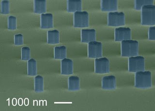
NIST researchers grow nanowires made of semiconductors—gallium nitride alloys—by depositing atoms layer-by-layer on a silicon crystal under high vacuum. NIST has the unusual capability to produce these nanowires without using metal catalysts, thereby enhancing luminescence and reducing defects. NIST nanowires also have excellent mechanical quality factors.
The latest experiments, described in Advanced Functional Materials,* maintained the purity and defect-free crystal structure of NIST nanowires while controlling diameter and placement better than has been reported by other groups for catalyst-based nanowires. Precise control of diameter and placement is essential before nanowires can be widely used.
The key trick in the NIST technique is to grow the wires through precisely defined holes in a stencil-like mask covering the silicon wafer.
NIST researchers analyzed micrographs to verify the uniformity of nanowire shape and size statistically. The analysis revealed nearly uniform areas of wires of the same diameter as well as nearly perfect hexagonal shapes.
Growing nanowires on silicon is one approach NIST researchers are exploring for making "nanowires on a chip" devices. Although the growth temperatures are too high—over 800 degrees Celsius—for silicon circuitry to tolerate, there may be ways to grow the nanowires first and then protect them during circuitry fabrication, lead author Kris Bertness says. The research was partially supported by the Defense Advanced Research Projects Agency (DARPA) Center on NanoscaleScience and Technology for Integrated Micro/Nano-Electromechanical Transducers (iMINT) at the University of Colorado at Boulder. ###
* K. A. Bertness, A. W. Sanders, D. M. Rourke, T. E. Harvey, A. Roshko, J.B. Schlager and N. A. Sanford. Controlled nucleation of GaN nanowires grown with molecular beam epitaxy. Advanced Functional Materials. Published online: July 13, 2010. DOI: 10.1002/adfm.201000381
Contact: Laura Ost laura.ost@nist.gov 303-497-4880 National Institute of Standards and Technology (NIST)


No comments:
Post a Comment