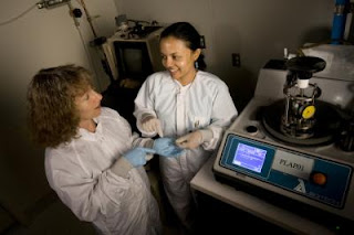
DURHAM, N.C. -- Step aside copper and make way for a better carrier of information -- light.
As good as the metal has been in zipping information from one circuit to another on silicon inside computers and other electronic devices, optical signals can carry much more, according to Duke University electrical engineers. So the engineers have designed and demonstrated microscopically small lasers integrated with thin film-light guides on silicon that could replace the copper in a host of electronic products.
The structures on silicon not only contain tiny light-emitting lasers, but connect these lasers to channels that accurately guide the light to its target, typically another nearby chip or component. This new approach could help engineers who, in their drive to create tinier and faster computers and devices, are studying light as the basis for the next generation information carrier.
The engineers believe they have solved some of the unanswered riddles facing scientists trying to create and control light at such a miniscule scale.
"The challenge has been creating light on such a small scale on silicon, and ensuring that it is received by the next component without losing most of the light," Palit said.
"We came up with a way of creating a thin film integrated structure on silicon that not only contains a light source that can be kept cool, but can also accurately guide the wave onto its next connection," she said. "This integration of components is essential for any such chip-scale, light-based system."
The Duke team developed a method of taking the thick substrate off of a laser, and bonding this thin film laser to silicon. The lasers are about one one-hundreth of the thickness of a human hair. These lasers are connected to other structures by laying down a microscopic layer of polymer that covers one end of the laser and goes off in a channel to other components. Each layer of the laser and light channel is given its specific characteristics, or functions, through nano- and micro-fabrication processes and by selectively removing portions of the substrate with chemicals.
"In the process of producing light, lasers produce heat, which can cause the laser to degrade," Sabarni said. "We found that including a very thin band of metals between the laser and the silicon substrate dissipated the heat, keeping the laser functional."
For Jokerst, the ability to reliably facilitate individual chips or components that "talk" to each other using light is the next big challenge in the continuing process of packing more processing power into smaller and smaller chip-scale packages.
"To use light in chip-scale systems is exciting," she said. "But the amount of power needed to run these systems has to be very small to make them portable, and they should be inexpensive to produce. There are applications for this in consumer electronics, medical diagnostics and environmental sensing." ###
The work on this project was conducted in Duke's Shared Materials Instrumentation Facility, which, like similar facilities in the semiconductor industry, allows the fabrication of intricate materials in a totally "clean" setting. Jokerst is the facility's executive director.
Other members of the team were Duke's Mengyuan Huang, as well as Dr. Jeremy Kirch and professor Luke Mawst from the University of Wisconsin at Madision.
Contact: Richard Merritt richard.merritt@duke.edu 919-660-8414 Duke University


No comments:
Post a Comment