Scalable and reusable optical detection system boasts the sensitivity of a large microscope in a much smaller, cheaper package.
CAMBRIDGE, Mass., February 15, 2009 -- With a silicone rubber "stick-on" sheet containing dozens of miniature, powerful lenses, engineers at Harvard are one step closer to putting the capacity of a large laboratory into a micro-sized package.
The marriage of high performance optics with microfluidics could prove the perfect match for making lab-on-a-chip technologies more practical.
Microfluidics, the ability to manipulate tiny volumes of liquid, is at the heart of many lab-on-a-chip devices. Such platforms can automatically mix and filter chemicals, making them ideal for disease detection and environmental sensing.

Caption: This is an example of multiple zone-plates placed over individual microfluidic channels.
Credit: Laboratory of Ken Crozier, Harvard School of Engineering and Applied Sciences. Usage Restrictions: None.

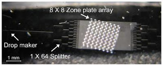
Caption: This is a microscope image of the microfluidic and optical device, consisting of a flow-focus drop maker, six layers of drop splitters, followed by 64 parallel microfluidic channels, and a zone-plate array which is aligned to the microfluidic channel array at a tilt angle.
Credit: The laboratory of Ken Crozier, Harvard School of Engineering and Applied Sciences. Usage Restrictions: None.

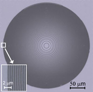
Caption: This is a zoom-in showing a single molded zone plate.
Credit: The laboratory of Ken Crozier, Harvard School of Engineering and Applied Sciences. Usage Restrictions: None. | The performance of these devices, however, is typically inferior to larger scale laboratory equipment. While lab-on-a-chip systems can deliver and manipulate millions of liquid drops, there is not an equally scalable and efficient way to detect the activity, such as biological reactions, within the drops.
The Harvard team's zone-plate array optical detection system, described in an article appearing in Lab on a Chip (Issue 5, 2010), may offer a solution. The array, which integrates directly into a massively parallel microfluidic device, can analyze nearly 200,000 droplets per second; is scalable and reusable; and can be readily customized.
"In essence, we've integrated some high performance optics onto a chip that contains microfluidics as well. This allows us to be able to parallelize the optics in the same way that a microfluidic device parallelizes sample manipulation and delivery," says Ken Crozier, an Associate Professor of Electrical Engineering at the Harvard School of Engineering and Applied Sciences (SEAS) who directed the research.
Unlike a typical optical detection system that uses a microscope objective lens to scan a single laser spot over a microfluidic channel, the team's zone-plate array is designed to detect light from multiple channels simultaneously. In their demonstration, a 62 element zone-plate array measured a fluorescence signal from drops traveling down 62 channels of a highly parallel microfluidic device.
The device works by creating a focused excitation spot inside each channel in the array and then collects the resulting fluorescence emission from water drops traveling through the channels, literally taking stop-motion pictures of the drops as they pass.
"Water drops flow through each channel of the device at a rate of several thousand per second," explains lead author Ethan Schonbrun, a graduate student at SEAS. "Each channel is monitored by a single zone plate that both excites and collects fluorescence from the high speed drops. By using large arrays of microfluidic channels and zone plate lenses, we can speed up microfluidic measurements."
The series of images are then recorded by a digital semiconductor (CMOS) camera, allowing high speed observation of all the channels simultaneously. Moreover, the array is designed so that each zone plate collects fluorescence from a well-defined region of the channel, thereby avoiding cross talk between adjacent channels. The end result is a movie of the droplets dancing through the channels. |
"Our approach allows us to make measurements over a comparatively large area over the chip. Most microscopes have a relatively limited view and cannot see how the whole system is working. With our device, we can place lenses wherever we want to make a measurement," adds Crozier.
The system can detect nearly 200,000 drops per second, or about four times the existing state-of-the-art detection systems. Further, the lens array is scalable, without any loss in efficiency, and can be peeled on-and-off like a reusable sticker. Ultimately, the integrated design offers the sensitivity of a larger confocal microscope and the ability to measure over a larger area, all in a much smaller, cheaper package.
"Because we have this massively parallel approach—effectively like 62 microscopes—we can get very high measurement or data rates," says Crozier. "This device has shown we can measure up to 200,000 drops per second, but I think we can push it even further."
Nanophotonics experts Schonbrun and Crozier originally developed the zone-plate technology to enhance optical tweezers so they could grab particles in a liquid using light. Using the high numerical aperture that makes efficient optical tweezers, they realized that arrays of zone plates could also be used to implement an efficient and scalable optical detection platform.
The researchers, who have filed a patent on their invention, are optimistic that with further research and development, the device could enhance a range of microfluidic and microfluidic-based lab-on-chip devices and speed the advance of using them for applications such as in-the-field biological assays. ###
Crozier and Schonbrun's co-authors included postdoctoral fellows Adam R. Abate and Paul E. Steinvurzel, both in SEAS, and David. A. Weitz, Mallinckrodt Professor of Physics and of Applied Physics, in SEAS and the Department of Physics at Harvard.
The authors acknowledge funding from the Defense Advanced Research Projects Agency. Fabrication work was carried out at the Center for Nanoscale Systems at Harvard, which is supported by the National Science Foundation.
Contact: Michael Patrick Rutter
mrutter@seas.harvard.edu 617-496-3815
Harvard University


No comments:
Post a Comment