Wednesday, April 29, 2009

Scientists prove graphene's edge structure affects electronic properties

CHAMPAIGN, Ill. — Graphene, a single-atom-thick sheet of carbon, holds remarkable promise for future nanoelectronics applications. Whether graphene actually cuts it in industry, however, depends upon how graphene is cut, say researchers at the University of Illinois.

Graphene consists of a hexagonal lattice of carbon atoms. While scientists have predicted that the orientation of atoms along the edges of the lattice would affect the material’s electronic properties, the prediction had not been proven experimentally.

Now, researchers at the U. of I. say they have proof.

nanometer scale piece of graphene on silicon

Atomic resolution scanning tunneling microscope image of a nanometer scale piece of graphene on silicon. Photo courtesy Joseph Lyding.
“Our experimental results show, without a doubt, that the crystallographic orientation of the graphene edges significantly influences the electronic properties,” said Joseph Lyding, a professor electrical and computer

“To utilize nanometer-size pieces of graphene in future nanoelectronics, atomically precise control of the geometry of these structures will be required.”
Lyding and graduate student Kyle Ritter (now at Micron Technology Inc. in Boise, Idaho) report their findings in a paper accepted for publication in Nature Materials. The paper was posted on the journal’s Web site on Sunday (Feb. 15).
To carry out their work, the researchers developed a method for cutting and depositing nanometer-size bits of graphene on atomically clean semiconductor surfaces like silicon.

Then they used a scanning tunneling microscope to probe the electronic structure of the graphene with atomic-scale resolution.


Electrical and computer engineering professor Joseph Lyding has proven that the orientation of atoms along the edges of the graphene lattice would affect the material’s electronic properties. Photo by L. Brian Stauffer
“From this emerged a clear picture that edges with so-called zigzag orientation exhibited a strong edge state, whereas edges with armchair orientation did not,” said Lyding, who also is affiliated with the university’s Beckman Institute and the Micro and Nanotechnology Laboratory.

“We found that pieces of graphene smaller than about 10 nanometers with predominately zigzag edges exhibited metallic behavior rather than the semiconducting behavior expected from size alone,” Lyding said. “This has major implications in that semiconducting behavior is mandatory for transistor fabrication.”

Unlike carbon nanotubes, graphene is a flat sheet, and therefore compatible with conventional fabrication processes used by today’s chipmakers. But, based on the researchers’ experimental results, controlled engineering of the graphene edge structure will be required for obtaining uniform performance among graphene-based nanoelectronic devices.

“Even a tiny section of zigzag orientation on a 5-nanometer piece of graphene will change the material from a semiconductor into a metal,” Lyding said. “And a transistor based on that, will not work. Period.”

The Office of Naval Research and the National Science Foundation funded the work.

Editor’s note: To reach Joseph Lyding, call 217-333-8370; e-mail: lyding@illinois.edu.

Contact: James E. Kloeppel, Physical Sciences Editor kloeppel@illinois.edu 217-244-1073 University of Illinois at Urbana-Champaign

Monday, April 27, 2009

Molecules Self-Assemble To Provide New Therapeutic Treatments

Researchers in the laboratory of Samuel I. Stupp at Northwestern University have an interesting approach for tackling some major health problems: gather raw materials and then let them self-assemble into structures that can address a multitude of medical needs.

At the core of the research are peptide amphiphiles (PA), small synthetic molecules that Stupp first developed seven years ago, which have been essential in his work on regenerative medicine. By tailoring these molecules and combining them with others, the researchers can make a wide variety of structures that may provide new treatments for medical issues including spinal cord injuries, diabetes and Parkinson's disease.

Ramille CapitoRamille M. Capito, a research assistant professor in Stupp's lab, shared an overview of this work in a presentation titled "Exploration of Novel Materials and Nanotubes in Stem Cell Therapy," Feb. 14, at the American Association for the Advancement of Science (AAAS) Annual Meeting in Chicago.
As a postdoctoral fellow in Stupp's group, Capito recently discovered that combining the PA molecules with hyaluronic acid (HA), a biopolymer readily found in the human body in places like joints and cartilage, resulted in an instant membrane structure in the form of self-assembling sacs. The sac membrane was found to have hierarchical order from the nanoscale to microscale giving it unique physical properties. These findings were first published last year in the journal Science (Capito et al, Science 2008; 319:1812-6).
In creating a sac, Capito took advantage of the fact that HA molecules are larger and heavier than the smaller PA molecules. In a deep vial, she pipetted the PA solution and onto that injected the HA solution. As the heavier molecules sank, the lighter molecules engulfed them, creating a closed sac with the HA solution trapped inside the membrane.Samuel Stupp
Having formed the sacs, Capito next studied human stem cells engulfed by the self-assembly process inside sacs that she placed in culture. She found that the cells remained viable for up to four weeks, that a large protein -- a growth factor important in the signaling of stem cells -- could cross the membrane, and that the stem cells were able to differentiate.

In a clever demonstration of self-repair, if the sac's membrane had a hole (from a needle injection, for example), Capito simply placed a drop of the PA solution on the tear, which interacted with the HA inside, resulting in self-assembly and a sealed hole.

While the underlying, highly ordered structures of the sacs and membranes have dimensions on the nanoscale, the sacs and membranes themselves can be of any dimension and are visible to the naked eye.

These sacs can be tailored to include bioactive regions, allowing researchers to incorporate a variety of designs into one sac structure. This capability opens the door to the creation of new methods for stem cell delivery. Stem cells can be loaded in the sac, which can be tailored to release the cells at the point of injury.

Previous work has shown that the PA molecules can be dissolved to form fibril structures with diameters of 5 to 8 nanometers. These gel structures can be used for regenerative medicine, and the research group has in vivo data for spinal cord repair, angiogenesis and bone and cartilage regeneration.

More information about research in the Stupp laboratory is available at stupp.northwestern.edu.

Contact: Megan Fellman fellman@northwestern.edu 847-491-3115 Northwestern University

Saturday, April 25, 2009

Nanoparticle toxicity doesn't get wacky at the smallest sizes

Big and small nanoparticles affect most genes similarly

CHICAGO – The smallest nano-sized silica particles used in biomedicine and engineering likely won't cause unexpected biological responses due to their size, according to work presented today. The result should allay fears that cells and tissues will react unpredictably when exposed to the finest silica nanomaterials in industrial or commercial applications.

Nanotoxicologist Brian Thrall and colleagues found that, mostly, size doesn't matter, by using total surface area as a measure of dose, rather than particle mass or number of particles, and observing how cultured cells responded biologically.

Brian D. Thrall, Ph.D.

Brian D. Thrall, Ph.D.
"If you consider surface area as the dose metric, then you get similar types of responses independent of the size of the particle," said Thrall, a scientist at the Department of Energy's Pacific Northwest National Laboratory in Richland, Wash. "That suggests the chemistry that drives the biological responses doesn't change when you get down to the smallest nanoparticle."
Nanoparticles are materials made up of spherical particles that are on average 100 to 1,000 times smaller than the width of a human hair. They are being used in tires, biomedical research, and cosmetics. Researchers are exploring these tiny spheres because their physical and chemical properties at that size offer advantages that standard materials don't, such as being able to float through blood vessels to deliver drugs.

But whether these materials are safe for human consumption is not yet clear. Previous work suggested, in some cases, nanoparticles become more toxic to cells the smaller the particles get.

Thrall presented this toxicology data on amorphous silica nanoparticles today at the 2009 American Association for the Advancement of Science's annual meeting. He also presented data on which cellular proteins the nanoparticles use to get inside cells.

One difficulty in measuring toxicity is that not everyone agrees which kind of dose unit to compare. Some researchers measure the dose by total weight, some by the number of particles. Neither method distinguishes whether a nanomaterial's toxicity is due to the inherent nature of the material or the particle size under scrutiny.

"Different dose metrics give different impressions of which particles are more toxic," he said.

To find out, Thrall and his colleagues at PNNL measured the dose at which the particles caused a biological response. The biological response was either death of the cell, or a change in which genes the cell turned on and off. They found that when calculating doses by particle number or mass, the amount needed to generate a biological response was all over the map.

They found that the best way to pinpoint how toxic the particles are to cells was to calculate the dose based on the total surface area of the nanomaterial. Only when they considered the surface area of the dose could they predict the biological response.

And the biological response, they found, was very similar regardless of the size of the nanoparticles. Inside cells, some genes responded to nanoparticles by ramping up or down. More than 76 percent of these genes behaved the same for all nanoparticle sizes tested. This indicated to the researchers that, for these genes, the nanoparticles didn't pick up weird chemical properties as they shrunk in size.

"The big fear is that you'd see unique biological pathways being affected when you get down to the nanoscale. For the most part, we didn't see that," said Thrall.

However, the team found some genes for which size did matter. A handful of genes, these fell into two categories: smaller particles appeared to affect genes that might be involved in inflammation. The larger particles appeared to affect genes that transport positively charged atoms into cells. This latter result could be due to metals contaminating the preparation of the larger particles, Thrall suggested.

Overall, the results contribute to a better understanding of what goes on at the nanoscale. # # #

Reference: Brian Thrall, "Systems Toxicology of Engineered Nanomaterials" during symposium titled Driving Beyond Our Nano-Headlights? Saturday, February 14, 8:30 am - 11:30 am at Hyatt Regency, Crystal Ballroom B, at the American Association for the Advancement of Science 2009 Annual Meeting, Chicago, Ill.

Pacific Northwest National Laboratory at the AAAS 2009 Meeting.

This work was supported by Laboratory-Directed Research and Development and then the National Institutes of Health.

Pacific Northwest National Laboratory is a Department of Energy Office of Science national laboratory where interdisciplinary teams advance science and technology and deliver solutions to America's most intractable problems in energy, national security and the environment. PNNL employs 4,200 staff, has a $850 million annual budget, and has been managed by Ohio-based Battelle since the lab's inception in 1965.

Contact: Mary Beckman mary.beckman@pnl.gov 509-375-3688 DOE/Pacific Northwest National Laboratory

Thursday, April 23, 2009

Nanogenerators produce electricity from running rodents and tapping fingers VIDEO

Hamster power, Could hamsters help solve the world's energy crisis? Probably not, but a hamster wearing a power-generating jacket is doing its own small part to provide a new and renewable source of electricity.

And using the same nanotechnology, Georgia Institute of Technology researchers have also generated electrical current from a tapping finger – moving the users of BlackBerry devices, cell phones and other handhelds one step closer to powering them with their own typing.

"Using nanotechnology, we have demonstrated ways to convert even irregular biomechanical energy into electricity," said Zhong Lin Wang, a Regent's professor in the Georgia Tech School of Materials Science and Engineering. "This technology can convert any mechanical disturbance into electrical energy."

The demonstrations of harnessing biomechanical energy to produce electricity were reported February 11 in the online version of the American Chemical Society journal Nano Letters. The research was supported by the Defense Advanced Research Projects Agency (DARPA), the U.S. Department of Energy, the U.S. Air Force, and the Emory-Georgia Tech Center for Cancer Nanotechnology Excellence.


The study demonstrates that nanogenerators – which Wang's team has been developing since 2005 – can be driven by irregular mechanical motion, such as the vibration of vocal cords, flapping of a flag in the breeze, tapping of fingers or hamsters running on exercise wheels. Scavenging such low-frequency energy from irregular motion is significant because much biomechanical energy is variable, unlike the regular mechanical motion used to generate most large-scale electricity today.

The nanogenerator power is produced by the piezoelectric effect, a phenomenon in which certain materials – such as zinc oxide wires – produce electrical charges when they are bent and then relaxed. The wires are between 100 and 800 nanometers in diameter, and between 100 and 500 microns in length.

To make their generators, Wang's research team encapsulated single zinc oxide wires in a flexible polymer substrate, the wires anchored at each end with an electrical contact, and with a Shottky Barrier at one end to control current flow. They then attached one of these single-wire generators to the joint area of an index finger, or combined four of the single-wire devices on a "yellow jacket" worn by the hamster.

The running and scratching of the hamster – and the tapping of the finger – flexed the substrate in which the nanowires were encapsulated, producing tiny amounts of alternating electrical current. Integrating four nanogenerators on the hamster's jacket generated up to up to 0.5 nanoamps; less current was produced by the single generator on the finger.
Hamster in Wheel

Caption: This image shows the hamster used to demonstrate conversion of biomechanical energy to electricity. Credit: Image courtesy of Zhong Lin Wang, Usage Restrictions: None.


Caption: This image shows a hamster wearing a jacket on which nanogenerators are attached. The generators produce electricity as the animal runs and scratches. Credit: Image courtesy Zhong Lin Wang. Usage Restrictions: None.
Wang estimates that powering a handheld device such as a Bluetooth headset would require at least thousands of these single-wire generators, which could be built up in three-dimensional modules.

Beyond the finger-tapping and hamster-running, Wang believe his modules could be implanted into the body to harvest energy from such sources as muscle movements or pulsating blood vessels. In the body, they could be used to power nanodevices to measure blood pressure or other vital signs.

Because the devices produce alternating current, synchronizing the four generators on the hamster's back was vital to maximizing current production. Without the synchronization, current flow from one generator could cancel out the flow from another.

The research team – which also included Rusen Yang, Yong Qin, Cheng Li and Guang Zhu – solved that problem by using a substrate that was flexible in only one direction, forcing the generators to flex together. Still, there was substantial variation in the output from each generator. The differences result from variations in the amount of flexing and from inconsistencies in the hand-built devices.

"The nanogenerators have to be synchronized, with the output of all of them coordinated so the current adds up constructively," Wang noted. "Through engineering, we would expect this can be resolved in the future through improved design and more consistent manufacturing."

To ensure that the current measured was actually produced by the generators, the researchers took several precautions. For instance, they substituted carbon fibers – which are not piezoelectric – for the zinc oxide nanowires and measured no output electrical signal.

The research team encountered a number of obstacles related to its four-legged subjects. Wang's team first tried to outfit a rat with the power-generating jacket, but found that the creature wasn't very interested in running.

At the suggestion of Wang's daughter, Melissa, the researchers found that hamsters are more active creatures – but only after 11 p.m. They had to experiment with a jacket configuration that was tight enough to stay on and to wrinkle the nanogenerator substrate – but not so tight as to make the hamster uncomfortable.

"We believe this is the first demonstration of using a live animal to produce current with nanogenerators," Wang added. "This study shows that we really can harness human or animal motion to generate current." ###

Technical Contact: Zhong Lin Wang (404-894-8008); E-mail: (zhong.wang@mse.gatech.edu).

Contact: John Toon jtoon@gatech.edu 404-894-6986 Georgia Institute of Technology Research News

Tuesday, April 21, 2009

Nanoparticle 'smart bomb' targets drug delivery to cancer cells

Researchers at North Carolina State University have successfully modified a common plant virus to deliver drugs only to specific cells inside the human body, without affecting surrounding tissue. These tiny "smart bombs" - each one thousands of times smaller than the width of a human hair - could lead to more effective chemotherapy treatments with greatly reduced, or even eliminated, side effects.

Drs. Stefan Franzen, professor of chemistry, and Steven Lommel, professor of plant pathology and genetics, collaborated on the project, utilizing the special properties of a fairly common and non-toxic plant virus as a means to convey drugs to the target cells.

The researchers say that the virus is appealing in both its ability to survive outside of a plant host and its built-in "cargo space" of 17 nanometers, which can be used to carry chemotherapy drugs directly to tumor cells.

Stefan Franzen Biophysical and Biological Chemistry ProfessorThe researchers deploy the virus by attaching small proteins, called signal peptides, to its exterior that cause the virus to "seek out" particular cells, such as cancer cells. Those same signal peptides serve as "passwords" that allow the virus to enter the cancer cell, where it releases its cargo.
"We had tried a number of different nanoparticles as cell-targeting vectors," Franzen says. "The plant virus is superior in terms of stability, ease of manufacture, ability to target cells and ability to carry therapeutic cargo."

Calcium is the key to keeping the virus' cargo enclosed. When the virus is in the bloodstream, calcium is also abundant. Inside individual cells, however, calcium levels are much lower, which allows the virus to open, delivering the cancer drugs only to the targeted cells.
Steven A. Lommel Professor of Plant Pathology
"Another factor that makes the virus unique is the toughness of its shell," Lommel says. "When the virus is in a closed state, nothing will leak out of the interior, and when it does open, it opens slowly, which means that the virus has time to enter the cell nucleus before deploying its cargo, which increases the drug's efficacy."

The researchers believe that their method will alleviate the side effects of common chemotherapy treatments, while maximizing the effectiveness of the treatment. ###

Contact: Tracey Peake tracey_peake@ncsu.edu 919-515-6142 North Carolina State University

Sunday, April 19, 2009

Major step for drug discovery and diagnostics

Researchers from Nano-Science Center, University of Copenhagen and National Centre for Scientific Research, France have developed a general method to study membrane proteins. This method can be used to screen several thousand proteins, and it will reduce the way from development to useful drugs substantially. Already now the pharmaceutical industry is interested and participate in a European consortium that is under construction. The research results are published in the prestigious scientific journal, PNAS.

Membrane proteins are located at the surface of cells and they have a very important role in the communication between the cells in our body. Defective membrane proteins are involved in diseases such as cancer, cardiovascular diseases and neurological diseases, just to mention at few. The researchers have developed a system, where they tie a tag to the protein that attach it to a surface and make it possible to investigate it in the laboratories.

Swimsuit for Proteins

Caption: This is an antibody recognizing a membrane protein dressed in an amphipol attached to a solid surface. Credit: Delphine Charvolin. Usage Restrictions: None.
Until now membrane proteins have been difficult to study when they are away from their natural environment in the cell, where there a belt of lipids surrounds them. This belt is essential for their survival and proper function.

Swimsuits for proteins with a tag

With our new method we can study membrane proteins faster and more accurate using less material than before. We are using a kind of swimsuit for the proteins called amphipols.
The amphipol substitute for the lipids, surround the membrane protein, and make it soluble in water while keeping its function intact. We attach a tag to the amphipol that will assemble to a surface like a key-lock system. When we have attached the proteins to a surface they can be adapted to several measuring instruments, says Associated Professor Karen Martinez, Department of Neuroscience and Pharmacology and Nano-Science Center at University of Copenhagen.

The researchers have tested their method on several different proteins and the results are very promising. When looking for new drugs, the researchers wants to study the interaction between membrane proteins and other molecules – e.g. potential drugs. It can also be used for the detection of virus, bacteria and parasites. A European consortium that is currently under construction, involving approximately 15 different laboratories, including both private companies and universities, will exploit the perspectives of this promising method.

Pharmaceutical industry interested

Our results indicate that the function of the tested proteins is not affected by the immobilisation. This makes it a general method that can be used for studying any membrane protein to virtually any surface. Membrane proteins involved in various diseases can be tested and our results can already now be used in the pharmaceutical industry to screen for new drugs and for diagnostics, says Dr. Jean-Luc Popot, head of the group at National Centre for Scientific Research and, in collaboration with R. Audebert and C. Tribet, the inventor of amphipols. ###

Link to paper in PNAS: www.pnas.org/content/

Contact: Gitte Frandsen gf@nano.ku.dk 452-875-0458 University of Copenhagen

Friday, April 17, 2009

New silver-based ink has applications in electronics

A new ink developed by researchers at the University of Illinois allows them to write their own silver linings.

The ink, composed of silver nanoparticles, can be used in electronic and optoelectronic applications to create flexible, stretchable and spanning microelectrodes that carry signals from one circuit element to another. The printed microelectrodes can withstand repeated bending and stretching with minimal change in their electrical properties.

In a paper published Feb. 12, by Science Express, the online version of the journal Science, Jennifer Lewis, the Thurnauer Professor of Materials Science and Engineering and director of the university's Frederick Seitz Materials Research Laboratory, and her collaborators demonstrate patterned silver microelectrodes by omnidirectional printing of concentrated nanoparticle inks with minimum widths of about 2 microns on semiconductor, plastic and glass substrates.

Jennifer A. Lewis

Jennifer A. Lewis, Hans Thurnauer Professor of Materials Science and Engineering
Willett Faculty Scholar.
"Unlike inkjet or screen printing, our approach enables the microelectrodes to be printed out-of-plane, allowing them to directly cross pre-existing patterned features through the formation of spanning arches," Lewis said. "Typically, insulating layers or bypass electrode arrays are required in conventional layouts."

To produce printed features, the researchers first prepare a highly concentrated silver nanoparticle ink. The ink is then extruded through a tapered cylindrical nozzle attached to a three-axis micropositioning stage, which is controlled by computer-aided design software.
When printed, the silver nanoparticles are not yet bonded together. The bonding process occurs when the printed structure is heated to 150 degrees Celsius or higher. During thermal annealing, the nanoparticles fuse into an interconnected structure. Because of the modest processing temperatures required, the printed features are compatible with flexible, organic substrates.

To demonstrate the versatility of the printing process, the researchers patterned both planar and out-of-plane silver microelectrodes; produced spanning interconnects for solar microcell and light-emitting-diode arrays; and bonded silver wires to fragile, three-dimensional devices.

"Unlike conventional techniques, our approach allows fine silver wires to be bonded to delicate devices using minimal contact pressure," said postdoctoral researcher Bok Yeop Ahn, the lead author of the paper.

"Our approach is capable of creating highly integrated systems from diverse classes of electronic materials on a broad range of substrates," said graduate student Eric Duoss, a co-author of the paper. "Omnidirectional printing overcomes some of the design constraints that have limited the potential of printed electronics."

In addition to Lewis, Ahn and Duoss, the paper's co-authors include chemistry professor Ralph Nuzzo and materials science and engineering professor John Rogers, as well as members of their research groups.

The work was funded by the U.S. Department of Energy.

Editor's note: To reach Jennifer Lewis, e-mail: jalewis@illinois.edu. To reach Ralph Nuzzo, email nuzzo@mrl.uiuc.edu.

Contact: James E. Kloeppel kloeppel@illinois.edu 217-244-1073 University of Illinois at Urbana-Champaign

Wednesday, April 15, 2009

Nanoscale materials grow with the flow VIDEO

Ames Lab physicist observes novel liquid-like motion and nucleation in metallic nanostructures.

Imagine unloading a pile of bricks onto the ground and watching the bricks assemble themselves into a level, straight wall in only a few minutes. While merely a fantasy for builders in the everyday world, these types of self-assembled structures are a reality for those who build materials in the nanoworld. Michael C. Tringides, a senior physicist at the U.S. Department of Energy's Ames Laboratory, has shown that nanoscale "straight wall" lead islands on silicon are spontaneously and quickly created by unusually mobile atoms.

Several years ago, Tringides' research group was the first to observe that lead atoms deposited on a silicon surface at low temperatures self-organize into uniform-height island nanostructures. The laws of quantum mechanics – specifically, Quantum Size Effects – determine why lead atoms stack up to create uniform islands while other nanostructure systems organize into islands that vary in height.

How the lead-on-silicon islands organized into uniform-height islands remained a mystery until Tringides' team made the surprising discovery that when lead atoms move along the surface of a silicon substrate, the lead atoms exhibit a liquid-like motion instead of the typical random-type diffusion observed in other systems.
The liquid-like motion of atoms was observed using scanning tunneling microscopy at Ames Lab and low energy electron microscopy performed by collaborators in Hong Kong.
"One big surprise was that the atoms were moving a lot at such a low temperature: 150 degrees Kelvin or minus 123 degrees Celsius," said Tringides. "The other surprise was that the atoms weren't moving randomly like individual atoms as we would expect. In this particular case, it seemed like the whole layer of lead atoms was moving like a liquid.
Fluid-like motion of the lead atoms explains why the layer moves so easily and forms uniform islands so quickly.

"When applying nanotechnology, it's very important to be able to make nanostructures of the same dimension using a method that others can easily replicate," said Tringides. "And, it's important that the growth process is fast."

Tringides' work succeeds in terms of uniformity and speed. The lead islands self-organize on silicon in only two to three minutes. Also, better understanding of how the lead islands grow will help researchers see if other systems show the same liquid-like behavior at low temperatures.

With such promising findings in hand, Tringides' team, which includes associate scientist Myron Hupalo and graduate students Steven Binz and Jizhou Chen, further investigated the possible use of these unusual lead islands on silicon as templates to study typical atomic processes, such as adsorption, nucleation and atom bonding. These processes are important in the study of reactivity and catalysis.

During those experiments, Tringides' group made another unexpected discovery. Normally atomic processes depend on an element's chemical nature, but the group found that when it came to lead islands, quantum mechanics had another surprise in store: The atomic processes depend dramatically on whether the island height is odd or even rather than its chemical nature. Tringides' group made this intriguing observation in a large lead island that had formed over a step on the original silicon surface. The top of the large island was flat as expected.

"But, the part of the island sitting on the higher terrace of silicon was four layers high, and the other part of the island sitting on the lower terrace was five layers," said Tringides.

The group studied nucleation on this unusual island by adding a very small amount of lead to its surface, creating many new small islands on top of the large island. Examination revealed that the density of the new islands was 60 times higher on the four-layer part of the island than on the five-layer part even though the two parts of the island were connected, suggesting that atom bonding is easier on the four-layer islands.

"The island was made up of the same element, lead, throughout," said Tringides. "So, we would expect the two parts of the island to communicate with each other, and atoms should be able to easily move from left to right and right to left among both halves of the island, so the density of the new small islands should have been the same in both parts."

Instead, the two halves of the island behaved like two separate islands. The four-layer section of the island has similar characteristics to independent four-layer islands, and the five-layer section behaved like other five-layer islands.

"For the purpose of growing materials, the two-part island indicates that we may not have to change the element to create variation in material properties," said Tringides. "Instead, we may be able to just change the height of the island."

"This is promising because it's easier to change the geometry of an island than to go out and find a new, exotic material," he added.

Tringides plans further experiments using gas adsorption to test the relationship between material reactivity and island height. ###

The Department of Energy's Office of Science, Basic Energy Sciences Office funded the work.

Ames Laboratory is a U.S. Department of Energy Office of Science research facility operated by Iowa State University. Ames Laboratory creates innovative materials, technologies and energy solutions. We use our expertise, unique capabilities and interdisciplinary collaborations to solve global challenges.

Contact: Breehan Gerleman Lucchesi breehan@ameslab.gov 515-294-9750 DOE/Ames Laboratory

Monday, April 13, 2009

Molecular machines drive plasmonic nanoswitches

University Park, Pa. — Plasmonics, a possible replacement for current computing approaches, may pave the way for the next generation of computers that operate faster and store more information than electronically-based systems and are smaller than optically-based systems, according to a Penn State engineer who has developed a plasmonic switch.

"If plasmonics are realized, the future will have circuits as small as the current electronic ones with a capacity a million times better," said Tony Jun Huang, James Henderson Assistant Professor of Engineering Science and Mechanics. "Plasmonics combines the speed and capacity of photonic — light based — circuits with the small size of electronic circuits."

Dr. Tony Jun Huang


Dr. Tony Jun Huang, James Henderson Assistant Professor. Department of Engineering, Science and Mechanics. Pennsylvania State University. 212 Earth-Engineering Sciences Building. University Park, PA 16802-6812.

Tel: 814-863-4209. Fax: 814-865-9974. Email: junhuang@psu.edu
Currently, electronic circuits can be made very small, but they are limited by their capacity and the speed that information can travel in the circuits. Optical circuits send information at the speed of light, but the size is large, limited by the light's wavelength. Plasmonics combines the best of electronic and optical circuits and can transmit electrons and light at the same time using the surface of the device.

Huang's team created a plasmonic switch from switchable bistable rotaxanes. Rotaxanes are complex molecules that consist of a dumbbell shape with a ring or rings encircling the shaft and are sometimes called molecular machines. The ring can either move from one end of the barbell to the other or rotate around the shaft. Changes in molecular shape are the basis of the plasmonic switch.

Computers, in their simplest form, are machines that can say yes or no multiple times to transfer information. The motion of a molecule can serve the same purpose as the on off switch on a light.
The researchers attached their molecular machines to gold-coated nanodiscs fabricated on glass. The machines were attached with disulfide functional groups. The dumbbell shaped molecules have two areas of the shaft primed with two different chemicals. The ring is initially drawn to circle at one primed area. When the chemical there is oxidized, the ring is repelled and moves to the other primed area, flipping the switch. The process is reversible, so the ring returns to its original state to switch on again later. When the molecule moves, it changes the surface plasmon resonance in that tiny area of the metal where it is attached. This change in resonance is what would send the signal on the circuit. The plasmonic switch that Huang and his team developed is not yet part of a circuit.

"Plasmonic circuits have not yet been achieved," said Huang. "In the past, the plasmonic devices made were all passive." These devices were used as light sources, lenses and waveguides

Huang's switches are activated by a chemical process, however, this is not the optimal choice for a working circuit.

"We believe that the chemically-driven redox process can be replaced with direct electrical or optical stimulation, a logical development that would establish a technological basis for the production of a new class of molecular-machine-based active plasmonic components for solid-state nanophotonic integrated circuits with the potential for low-energy and ultra small operations," the researchers state in a recent issue of Nano Letters.

In essence, plasmonic devices would allow computers to get faster and have more memory storage in smaller spaces. Storage of as much as 1,000 movies on a typical USB drive would be possible. Huang suggests that applications like YouTube, which are very popular but have terrible resolution, could become places to see high-resolution images.

"We are in the very beginning of this field," said Huang. "Creation of a plasmonic circuit is probably five years away."

Besides Huang, researchers on this project include Yue Bing Zheng and Bala Krishna Juluri, graduate students in Engineering Science and Mechanics; Lasse Jensen, professor of chemistry; Paul Weiss, distinguished professor of chemistry and physics, all at Penn State; Lei Fang, graduate student and J. Fraser Stoddart, professor, Northwestern University; Ying-Wei yang, postdoctoral fellow, University of California, Los Angeles and Amar H. Flood, professor, Indiana University. The U.S. Air Force Office of Scientific Research and the National Science Foundation supported this work.

Contact: A'ndrea Elyse Messer aem1@psu.edu 814-865-9481 Penn State

Saturday, April 11, 2009

Viscosity-enhancing nanomaterials may double service life of concrete

Engineers at the National Institute of Standards and Technology (NIST) are patenting a method that is expected to double the service life of concrete. The key, according to a new paper*, is a nano-sized additive that slows down penetration of chloride and sulfate ions from road salt, sea water and soils into the concrete. A reduction in ion transport translates to reductions in both maintenance costs and the catastrophic failure of concrete structures. The new technology could save billions of dollars and many lives.

Concrete has been around since the Romans, and it is time for a makeover. The nation’s infrastructure uses concrete for millions of miles of roadways and 600,000 bridges, many of which are in disrepair. In 2007, 25 percent of U.S. bridges were rated as structurally deficient or functionally obsolete, according to the Federal Highway Administration. Damaged infrastructure also directly affects large numbers of Americans’ own budgets. The American Society of Civil Engineers estimates that Americans spend $54 billion each year to repair damages caused by poor road conditions.

Viscosity-Enhancing Nanomaterials

Caption: The barely visible blue-green area at the top of this X-ray image of concrete with the NIST nanoadditive shows that very few chloride ions (in green) penetrate into the concrete.

Credit: NIST. Usage Restrictions: None.
Infiltrating chloride and sulfate ions cause internal structural damage over time that leads to cracks and weakens the concrete.

Past attempts to improve the lifetime of concrete have focused on producing denser, less porous concretes, but unfortunately these formulations have a greater tendency to crack. NIST engineers took a different approach, setting out to double the material’s lifetime with a project called viscosity enhancers reducing diffusion in concrete technology (VERDICT).

Rather than change the size and density of the pores in concrete, they reasoned, it would be better to change the viscosity of the solution in the concrete at the microscale to reduce the speed at which chlorides and sulfates enter the concrete. “Swimming through a pool of honey takes longer than making it through a pool of water,” engineer Dale Bentz says.
They were inspired by additives the food processing industry uses to thicken food and even tested out a popular additive called xanthum gum that thickens salad dressings and sauces and gives ice cream its texture.

Studying a variety of additives, engineers determined that the size of the additive’s molecule was critical to serving as a diffusion barrier. Larger molecules such as cellulose ether and xanthum gum increased viscosity, but did not cut diffusion rates. Smaller molecules—less than 100 nanometers—slowed ion diffusion. Bentz explains, “When additive molecules are large but present in a low concentration, it is easy for the chloride ions to go around them, but when you have a higher concentration of smaller molecules increasing the solution viscosity, it is more effective in impeding diffusion of the ions.”

The NIST researchers have demonstrated that the additives can be blended directly into the concrete with current chemical admixtures, but that even better performance is achieved when the additives are mixed into the concrete by saturating absorbant, lightweight sand. Research continues on other materials as engineers seek to improve this finding by reducing the concentration and cost of the additive necessary to double the concrete's service life. ###

A non-provisional patent application was filed in September, and the technology is now available for licensing from the U.S. government; the NIST Office of Technology Partnerships can be contacted for further details (Contact: Terry Lynch, terry.lynch@nist.gov, (301) 975-2691).

* D.P. Bentz, M.A. Peltz, K.A. Snyder and J.M. Davis. VERDICT: Viscosity Enhancers Reducing Diffusion in Concrete Technology. Concrete International. 31 (1), 31-36, January 2009.

Contact: Evelyn Brown evelyn.brown@nist.gov 301-975-5661 National Institute of Standards and Technology (NIST)

Thursday, April 09, 2009

Taking the stress out of magnetic field detection

Researchers at the National Institute of Standards and Technology (NIST) have discovered that a carefully built magnetic sandwich that interleaves layers of a magnetic alloy with a few nanometers of silver “spacer” has dramatically enhanced sensitivity—a 400-fold improvement in some cases. This material could lead to greatly improved magnetic sensors for a wide range of applications from weapons detection and non-destructive testing to medical devices and high-performance data storage.

Those applications and many others are based on thin films of magnetic materials in which the direction of magnetization can be switched from one orientation to another. An important characteristic of a magnetic film is its saturation field, the magnitude of the applied magnetic field that completely magnetizes the film in the same direction as the applied field—the smaller the saturation field, the more sensitive the device.

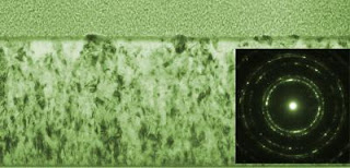
transmission electron microscope image

Caption: This transmission electron microscope image shows sections of a continuous 400-nanometer-thick magnetic film of a nickle-iron-copper-molybdenum alloy layered with silver every 100 nanometers. By relieving strain in the film, the silver layers promote the growth of notably larger crystal grains in the layered material as compared to the monolithic film (several are highlighted for emphasis). Electron diffraction patterns (insets) tell a similar story: the material with larger crystal grains display sharper, more discrete scattering patterns.

Credit: Credit: Bonevich, NIST. Usage Restrictions: None.
The saturation field is often determined by the amount of stress in the film—atoms under stress due to the pull of bonds with neighboring atoms are more resistant to changing their magnetic orientation. Metallic films develop not as a single monolithic crystal, like diamonds, but rather as a random mosaic of microscopic crystals called grains.

Atoms on the boundaries between two different grains tend to be more stressed, so films with a lot of fine grains tend to have more internal stress than coarser grained films. Film stress also increases as the film is made thicker, which is unfortunate because thick films are often required for high magnetization applications.
The NIST research team discovered that magnetic film stress could be lowered dramatically by periodically adding a layer of a metal, having a different crystal structure or lattice spacing, in between the magnetic layers. Although the mechanism isn’t completely understood, according to lead author William Egelhoff Jr., the intervening layers disrupt the magnetic film growth and induce the creation of new grains that grow to be larger than they do in the monolithic films.transmission electron microscope image

Caption: This transmission electron microscope image shows sections of a continuous 400-nanometer-thick magnetic film of a nickle-iron-copper-molybdenum alloy.

Credit: Credit: Bonevich, NIST. Usage Restrictions: None.
The researchers prepared multilayer films with layers of a nickel-iron-copper-molybdenum magnetic alloy each 100 nanometers (nm) thick, interleaved with 5-nm layers of silver. The structure reduced the tensile stress (over a monolithic film of equivalent thickness) by a factor of 200 and lowered the saturation field by a factor of 400. ###

The work has particular application in the design of “flux concentrators,” magnetic structures that draw in external magnetic field lines and concentrate them in a small region. Flux concentrators are used to amplify fields in compact magnetic sensors used for a wide variety of applications.

* W.F. Egelhoff, Jr., J. Bonevich, P. Pong, C.R. Beauchamp, G.R. Stafford, J. Unguris, and R.D. McMichael. 400-fold reduction in saturation field by interlayering. J. Appl. Phys. 105, 013921 (2009). Published online Jan. 13, 2009. DOI:10.1063/1.3058673

Contact: Michael Baum michael.baum@nist.gov 301-975-2763 National Institute of Standards and Technology (NIST)

Tuesday, April 07, 2009

Yale engineers revolutionize nano-device fabrication using amorphous metals

New Haven, Conn. — Yale engineers have created a process that may revolutionize the manufacture of nano-devices from computer memory to biomedical sensors by exploiting a novel type of metal. The material can be molded like plastics to create features at the nano-scale and yet is more durable and stronger than silicon or steel. The work is reported in the February 12 issue of Nature.

The search for a cost-effective and manageable process for higher-density computer chip production at the nano-scale has been a challenge. One solution is making nano-scale devices by simple stamping or molding, like the method used for fabricating CDs or DVDs. This however requires stamps or master molds with nano-scale features. While silicon-based molds produce relatively fine detail, they are not very durable. Metals are stronger, but the grain size of their internal structure does not allow nano-scale details to be imprinted on their surfaces.

Parts Fabricated by Molding Metallic Glass

Caption: Various parts (nano-molds, nano-wires, gears, membrane, scalpels, and tweezers) fabricated by molding metallic glass over wide range of length scales -- from 13 nm to several millimeters.

Credit: Kumar/Schroers(Yale). Usage Restrictions: Credit required.
Unlike most metals, “amorphous metals” known as bulk metallic glasses (BMGs) do not form crystal structures when they are cooled rapidly after heating. Although they seem solid, they are more like a very slow-flowing liquid that has no structure beyond the atomic level — making them ideal for molding fine details, said senior author Jan Schroers of the Yale School of Engineering & Applied Science.
Researchers have been exploring the use of BMGs for about a decade, according to Schroers. “We have finally been able to harness their unusual properties to transform both the process of making molds and producing imprints,” he said. “This process has the potential to replace several lithographic steps in the production of computer chips.”

Schroers says BMGs have the pliability of plastics at moderately elevated temperatures, but they are stronger and more resilient than steel or metals at normal working temperatures.

“We now can make template molds that are far more reliable and lasting than ones made of silicon and are not limited in their detail by the grain size that most metals impose,” said Schroers.

To actually get detail at the nano-scale the researchers had to overcome an issue faced in any molding process — how to get the material to cover the finest detail, and then how to separate the material intact from the mold. Surfaces of liquid metals exhibit high surface tension and capillary effects that can interfere in the molding.

Postdoctoral fellow Golden Kumar found that by altering the mold-BMG combination they could create surfaces so that the atoms take advantage of their favorable interaction with the mold— to both fill the mold and then release the product.

In this paper, Schroers’ team reports nano-patterning of details as small as 13 nanometers— about one ten-thousandth the thickness of a human hair — and the scientists expect that even finer detail will be possible since the BMGs are only limited by the size of a single atom.

While ‘plastics!’ was the catchword of the 1960’s, Schroers says, “We think ‘BMGs!’ will be the buzz-word for the coming decade.” ###

Hong Tang, assistant professor of mechanical engineering and electrical engineering at Yale was also an author of the paper. Funding for this research was from the National Science Foundation

Jan Schroers www.seas.yale.edu/faculty-detail
Yale School of Engineering& Applied Science www.seas.yale.edu/home
Golden Kumar www.eng.yale.edu/content/
Hong Tang www.seas.yale.edu/faculty-detail

Contact: Janet Rettig Emanuel janet.emanuel@yale.edu 203-432-2157 Yale University

Sunday, April 05, 2009

Research Highlights Potential for Improved Solar Cells

LOS ALAMOS, N.M., — Certain nanocrystals shown to generate more than one electron after absorbing a single photon.

A team of Los Alamos researchers led by Victor Klimov has shown that carrier multiplication—when a photon creates multiple electrons—is a real phenomenon in tiny semiconductor crystals and not a false observation born of extraneous effects that mimic carrier multiplication.

The research, explained in a recent issue of Accounts of Chemical Research, shows the possibility of solar cells that create more than one unit of energy per photon.

Questions about the ability to increase the energy output of solar cells have prompted Los Alamos National Laboratory researchers to reassess carrier multiplication in extremely small semiconductor particles.

carrier multiplication Solar CellsWhen a conventional solar cell absorbs a photon of light, it frees an electron to generate an electrical current. Energy in excess of the amount needed to promote an electron into a conducting state is lost as heat to atomic vibrations (phonons) in the material lattice.
Through carrier multiplication, excess energy can be transferred to another electron instead of the material lattice, freeing it to generate electrical current—thereby yielding a more efficient solar cell.

Klimov and colleagues have shown that nanocrystals of certain semiconductor materials can generate more than one electron after absorbing a photon. This is partly due to strengthened interactions between electrons squeezed together within the confines of the nanoscale particles.

In 2004, Los Alamos researchers Richard Schaller and Klimov reported the first observations of strong carrier multiplication in nanosized crystals of lead selenide resulting in up to two electron-hole pairs per absorbed photon. A year later, Arthur Nozik and coworkers at the National Renewable Energy Laboratory reproduced these results. Eventually, spectroscopic signatures of carrier multiplication were observed in nanocrystals of various compositions, including silicon.

Recently, the claims in carrier multiplication research have become contentious. Specifically, some recent studies described low or negligible carrier multiplication efficiencies, which seemed to run contrary to earlier findings. To sort out these discrepancies, Los Alamos researchers analyzed factors that could have led to a spread in the reported carrier multiplication results. These factors included variations between samples, differences in detection techniques, and effects mimicking the signatures of carrier multiplication in spectroscopic measurements.

To analyze how a particular detection technique might affect an outcome, John McGuire, a postdoctoral researcher on Klimov’s team, investigated carrier multiplication using two different spectroscopic techniques—transient absorption and time-resolved photoluminescence. The results obtained by these two methods were in remarkable agreement, indicating that the use of different detection techniques is unlikely to explain discrepancies highlighted by other researchers. Further, although these measurements revealed some sample-to-sample variation in carrier multiplication yields, these variations were much smaller than the spread in reported data.

After ruling out these two potential causes of discrepancies, the researchers focused on effects that could mimic carrier multiplication. One such effect is photoionization of nanocrystals.

“When a nanocrystal absorbs a high-energy photon, an electron can acquire enough energy to escape the material,” Klimov explained. “This leaves behind a charged nanocrystal, which contains a positive ‘hole.’ Photogeneration of another electron by a second photon results in a two-hole, one-electron state, reminiscent of one produced by carrier multiplication, which can lead to false positives,” he said.

To evaluate the influence of photoionization, the Los Alamos researchers conducted back-to-back studies of static and stirred solutions of nanocrystals. Stirring removes charged nanocrystals from the measured region of the sample. Therefore, when crystals are subjected to light, the stirring eliminates the possibility that charged nanocrystals will absorb a second photon. While stirring of some samples did not affect the results of the measurements, other samples showed a significant difference in the apparent carrier multiplication yields measured under static and stirred conditions. Since most previous studies were performed on static samples, these results suggest that discrepancies noted by other researchers arise at least in part from uncontrolled photoionization, which stirring seeks to eliminate.

The Los Alamos researchers re-evaluated carrier multiplication efficiencies when photoionization was suppressed. The results are encouraging.

While the newly measured electron yields are lower than previously reported, the efficiency of carrier multiplication is still greater than in bulk solids. Specifically, both the energetic onset and the energy required to generate an extra electron in nanocrystals are about half of those in bulk solids.

These results indicate significant promise for nanosized crystals as efficient harvesters of solar radiation.

“Researchers still have a lot of work to do,” Klimov cautioned. “One important challenge is to figure out how to design a material in which the energetic cost to create an extra electron can approach the limit defined by a semiconductor band gap. Such a material could raise the fundamental power conversion limit of a solar cell from 31 percent to above 40 percent.”

The Los Alamos nanocrystal team’s research is funded by the U.S. Department of Energy Office of Basic Energy Sciences and Los Alamos’ Laboratory-Directed Research and Development (LDRD) program.

About Los Alamos National Laboratory (www.lanl.gov)

Los Alamos National Laboratory, a multidisciplinary research institution engaged in strategic science on behalf of national security, is operated by Los Alamos National Security, LLC, a team composed of Bechtel National, the University of California, The Babcock & Wilcox Company, and the Washington Division of URS for the Department of Energy's National Nuclear Security Administration.

Los Alamos enhances national security by ensuring the safety and reliability of the U.S. nuclear stockpile, developing technologies to reduce threats from weapons of mass destruction, and solving problems related to energy, environment, infrastructure, health, and global security concerns.

For more information on the research team, visit: quantumdot.lanl.gov/.

Contact: James E. Rickman jamesr@lanl.gov 505-665-9203 DOE/Los Alamos National Laboratory

Friday, April 03, 2009

Carbon nanotube avalanche process nearly doubles current

CHAMPAIGN, Ill. — By pushing carbon nanotubes close to their breaking point, researchers at the University of Illinois have demonstrated a remarkable increase in the current-carrying capacity of the nanotubes, well beyond what was previously thought possible.

The researchers drove semiconducting carbon nanotubes into an avalanche process that carries more electrons down more paths, similar to the way a multilane highway carries more traffic than a one-lane road.

“Single-wall carbon nanotubes are already known to carry current densities up to 100 times higher than the best metals like copper,” said Eric Pop, a professor of electrical and computer engineering at the U. of I. “We now show that semiconducting nanotubes can carry nearly twice as much current as previously thought.

professor Eric Pop, from left, worked with undergraduate Yang Zhao and graduate student Albert Liao

Electrical and computer engineering professor Eric Pop, from left, worked with undergraduate Yang Zhao and graduate student Albert Liao, both in ECE, to demonstrate a remarkable increase in the current-carrying capacity of carbon nanotubes. Photo by L. Brian Stauffer
As reported in the journal Physical Review Letters, the researchers found that at high electric fields (10 volts per micron), energetic electrons and holes can create additional electron-hole pairs, leading to an avalanche effect where the free carriers multiply and the current rapidly increases until the nanotube breaks down.

The sharp increase in current, Pop said, is due to the onset of avalanche impact ionization, a phenomenon observed in certain semiconductor diodes and transistors at high electric fields, but not previously seen in nanotubes.

While the maximum current carrying capacity for metallic nanotubes has been measured at about 25 microamps, the maximum current carrying capacity for semiconducting nanotubes is less established. Previous theoretical predictions suggested a similar limit for single-band conduction in semiconducting nanotubes.
To study current behavior, Pop, graduate student Albert Liao and undergraduate student Yang Zhao first grew single-wall carbon nanotubes by chemical vapor deposition from a patterned iron catalyst. Palladium contacts were used for measurement purposes. The researchers then pushed the nanotubes close to their breaking point in an oxygen-free environment.

“We found that the current first plateaus near 25 microamps, and then sharply increases at higher electric fields,” said Pop, who also is affiliated with the Beckman Institute and the Micro and Nanotechnology Laboratory at the U. of I. ”We performed repeated measurements, obtaining currents of up to 40 microamps, nearly twice those of previous reports.”

By inducing very high electric fields in the nanotubes, the researchers drove some of the charge carriers into nearby subbands, as part of the avalanche process. Instead of being in just one “lane,” the electrons and holes could occupy several available lanes, resulting in much greater current.

The avalanche process (which cannot be observed in metallic carbon nanotubes because an energy gap is required for electron-hole multiplication) offers additional functionality to semiconducting nanotubes, Pop said. “Our results suggest that avalanche-driven devices with highly nonlinear turn-on characteristics can be fashioned from semiconducting single wall nanotubes.”

Funding was provided by the National Science Foundation and the National Institute of Standards and Technology through the Nanoelectronics Research Initiative.

Editor’s note: To reach Eric Pop, call 217-244-2070; e-mail

Contact: James E. Kloeppel, Physical Sciences Editor kloeppel@illinois.edu 217-244-1073 University of Illinois at Urbana-Champaign