Tuesday, March 31, 2009

GoNano Technologies Awarded a Phase I SBIR Grant to Develop Novel Ultracapacitor Electrodes

Revolutionary Nanospring™ Technology Key to Enhanced Energy Density

Moscow, ID – March 24, 2009 – GoNano Technologies, Inc., a Moscow, Idaho based nanotechnology company specializing in the development of high surface area Nanospring™ technology, recently received a Phase I SBIR grant in the amount of $97,761 from the National Science Foundation to develop novel electrodes for next generation ultracapacitors.

“This Phase I SBIR award will generate valuable information on the integration of nanomaterials into energy storage devices with broader technological implications for battery and fuel cell electrodes,” said Dr. David McIlroy, Vice President-Research at GoNano Technologies. “Additionally, new knowledge will be developed about how to best functionalize one-dimensional nanostructures and how processes can be appropriately scaled.”

David N. McIlroy

David N. McIlroy Professor of Physics Experimental Condensed Matter Physics. Contact information: University of Idaho Department of Physics Rm EP 325 Moscow, ID 83844-0903. Tel: 208.885.6809, Fax: 208.885.4055, Email: dmcilroy@uidaho.edu
The key to ultracapacitor design is a high surface area electrode material because this material determines energy capacity. GoNano Technologies, Inc will use their patent-pending Nanospring mats as a low cost, high surface area scaffolding for constructing ultracapacitor electrodes. Optimizing the properties of ultracapacitors through the integration of nanostructured materials with high surface area and controlled surface chemistry will allow more widespread implementation of this technology.
“With higher energy density and a lower cost than conventional electrodes, GoNano’s Nanospring™ technology overcomes two long-standing market barriers”, said Tim Kinkeade, CEO of GoNano Technologies. “This scalable, efficient, and industry compatible system is of significant interest to ultracapacitor manufacturers everywhere.”

About GoNano Technologies

GoNano develops and manufactures environmentally friendly high surface area nanomaterials for Energy Storage and Catalytic Processing. Our patent pending nanomaterials provide a scalable, industry compatible, low cost platform for highly efficient solutions. More information can be found at www.gonano-9.com. GoNano Technologies, Inc can be reached at 208 892 2000.

CONTACT: Tim Kinkeade. CEO GoNano Technologies, Inc 208-892-2000 tk@gonano-9.com

Sunday, March 29, 2009

Accidental discovery has potential for new applications in packaging

Case Western Reserve University polymer research may help keep food and drugs safer and other materials fresher longer

CLEVELAND – A recent discovery at Case Western Reserve University may help keep food and drugs safer and fresher longer and electronic equipment dryer and more secure than ever before – all at a lower cost.

The finding involves a nanotechnology-based technique to block the transport of damaging gases through a polymer, making it stronger while using less material. It was made in the labs of the National Science Foundation-supported Center for Layered Polymeric Systems (CLiPS) at the Case School of Engineering. The findings are published in the Feb. 6, 2009, issue of the journal Science.

Anne Hiltner

Anne Hiltner, The Herbert Henry Dow Professor. Ph.D. Physical Chemistry. Oregon State University, 1967

Room 423 Phone: (216) 368-4186. Fax: (216) 368-4202. Email: pah6@case.edu
"This work takes a step toward developing more flexible, optically transparent, ultra-high barrier polymers for several different applications," said Anne Hiltner, lead author of the study and the Herbert Henry Dow Professor of Science and Engineering at Case Western Reserve. She also serves as lead investigator and co-director of CLiPS.

The discovery was a serendipitous find, according to Hiltner. The researchers found that when confined as nanolayers, polyethylene oxide (PEO) crystallizes as a single layer, resembling very large, impermeable single crystals that reduce by 100 times the amount of gas permeability in all kinds of polymer-based applications. When a crystallizable polymer is confined to such thin layers, it surprised the researchers by spontaneously organizing themselves into a nearly perfect crystalline packing of the polymer chains in each thin layer, Hiltner says.
Crystalline regions of polymers are areas where the atoms in polymer chains line up relative to one another in a rigorous and well-defined, ordered pattern, much like water molecules align next to each other in a well-defined pattern in ice (which is, in fact, crystalline water). Because the atoms are closely aligned to each other in a regular pattern, crystalline regions of polymers do not permit the transport through them of even the smallest gas molecules, such as oxygen or carbon dioxide. Thus, crystalline regions of polymers decrease the permeability of gases through such polymers – that is, crystalline regions improve barrier properties of polymers.

"To find something as unexpectedly as we did is the kick you get out of exploring," Hiltner said.

This spontaneous organization of a polymer melt into large (in terms of length and width), nearly perfect, so-called single crystals has not been observed before this study, according to Benny Freeman, the Kenneth A. Kobe Professor of Chemical Engineering at the University of Texas at Austin and co-author of the study.

"The ability to produce literally kilometers of film containing single crystals of polymer is unprecedented," Freeman said.

Crystalline polymers, such as polyethylene, polypropylene and nylon, have been broadly used as gas barrier films in food, medicine and electronics packaging, benefitting from their low cost, easy processing and mechanical toughness.

Using an innovative layer-multiplying co-extrusion process that takes two polymer melts and combines them as layers, multiplies the layers to four, and doubles that again as many times as desired, the research team discovered that a new structure emerges as confined polyethylene oxide (PEO) layers are made progressively thinner, thereby saving material.

Polymers are already used in many applications where their ability to keep wrapping tightly sealed is critically important to the performance of the application, such as in food and medicine packaging. Yet there are emerging technologies, such as flexible electronic displays, where the barriers of current polymers are not sufficient to meet the needs of the application. ###

About the Center for Layered Polymeric Systems (CLiPS)

Established by a five-year, $19 million grant from the National Science Foundation, the Center for Layered Polymeric Systems is a powerful new national presence for research at the intersection of polymer science and engineering and the physical sciences (called "Polymers Plus"). It also plays an important role in educating a diverse American workforce to meet the challenges of emerging multidisciplinary polymer-based technologies. To create CLiPS, Case Western Reserve University partnered with the University of Texas at Austin, Fisk University, the University of Southern Mississippi and the Naval Research Laboratory.

Contact: Laura M. Massie laura.massie@case.edu 216-368-4442 Case Western Reserve University

Friday, March 27, 2009

Scientists can predict nano drug outcome

Scientists including one from The University of Texas Health Science Center at Houston successfully predicted the outcome of a nano drug on breast tumors in a pre-clinical study. Their research could help determine which patients will respond best to cancer-fighting nano drugs.

Researchers from the Georgia Institute of Technology and Emory University also participated in the study, which appears in the February issue of Radiology.

The investigators used contrast agents encapsulated in tiny fat bubbles called liposomes to determine if breast tumors in rodents could be breached by liposomes loaded with a cancer drug called liposomal doxorubicin. The liposomes were administered intravenously.

When scientists X-rayed the rodents, the investigators received good images of porous breast tumors which had absorbed the contrast agents. On the other hand, poor images indicated the contrast agents had not substantially penetrated the tumor. When liposomal doxorubicin was administered, it was associated with better therapeutic results in the tumors with superior images.

Ananth Annapragada Ph.D

Ananth Annapragada Ph.D
"We can tell if the animals are candidates for the treatment or not," said Ananth Annapragada Ph.D., one of two senior authors and an associate professor at The University of Texas School of Health Information Sciences at Houston.

Higher uptake of the probe by the tumor, indicating leakier vasculature, was associated with a slower tumor growth rate,
suggesting a better therapeutic outcome with liposomal doxorubicin, the authors wrote. A nanometer is a billionth of a meter and a liposome is about 100 nanometers.

Nano drugs for cancer like liposomal doxorubicin are designed to increase the amount of drug reaching tumors. Currently, when an intravenous cancer drug is administered, very little reaches its intended target. The remaining drug circulates in the bloodstream and can cause side effects.

Liposomes carrying drugs infiltrate leaky tumors that have pores up to eight times the size of these miniaturized drug carriers. If a liposome with contrast agents can penetrate a tumor and be detected by X-rays, there is a good chance that a liposome with anti-cancer agents can enter the tumor, too. "We found that different tumors light up differently. The tumors that light up well take up the agent. Consequently, these are the tumors most likely to respond to liposomal doxorubicin," Annapragada said.

The current clinical protocols for liposomal doxorubicin consist of a standard dose every three to four weeks, the authors wrote. No prior knowledge of tumor vessel status, especially leakiness, is taken into account for the dose scheduling. However, it is well known that the degree of tumor vasculature leakiness differs not only among same-type tumors, but even spatially in the same tumor.

"This new information could help personalize the treatment of cancer with liposomal doxorubicin," Annapragada said.

In addition to predicting the outcome of liposomal doxorubicin on breast tumors, liposomes can be used for live monitoring of anti-cancer agents in action. When loaded with both contrast agents and liposomal doxorubicin, the liposomes provide information on tumor leakiness, which can be used in tumor prognostication. A pre-clinical study on multi-functional liposomes by many of the same researchers was published in Biomaterials in December.

Annapragada and the study's other senior author, Ravi V. Bellamkonda, Ph.D., of the Georgia Institute of Technology/Emory University, are involved in a UT Health Science Center at Houston portfolio start-up company called Marval Biosciences that is working to translate these enhanced medical imaging techniques into patient diagnostics. ###

Lead author Efstathios Karathanasis, Ph.D., is a former student of Annapragada and now a postdoctoral fellow at the Georgia Institute of Technology/Emory University. Other collaborators from the Georgia Institute of Technology/Emory University include Sri Balusu and Kathleen McNeeley. Researchers from the Department of Radiology and Winship Cancer Institute include Sankararaman Suryanarayanan, Ph.D.; Ioannis Sechopoulos, Ph.D.; and Andrew Karellas, Ph.D.

The study, titled "Imaging Nanoprobe for Prediction of Outcome of Nanoparticle Chemotherapy by Using Mammography," was supported by the Georgia Cancer Coalition and the National Science Foundation. Radiology is a publication of the Radiological Society of North America.

Annapragada is also on the faculty of The University of Texas Graduate School of Biomedical Sciences at Houston, the Keck Institute for Computational and Structural Biology, The University of Houston, Rice University and The University of Texas at Austin.

Contact: Robert Cahill Robert.Cahill@uth.tmc.edu 713-500-3042 University of Texas Health Science Center at Houston

Wednesday, March 25, 2009

Nanotube's 'tapestry' controls its growth

PNAS study answers longstanding mystery about carbon nanomaterials

HOUSTON -- Rice University materials scientists have put a new "twist" on carbon nanotube growth. The researchers found the highly touted nanomaterials grow like tiny molecular tapestries, woven from twisting, single-atom threads.

Carbon nanotubes are hollow tubes of pure carbon that measure about one nanometer, or one-billionth of a meter, in diameter. In molecular diagrams, they look like rolled-up sheets of chicken wire. And just like a roll of wire or gift-wrapping paper, nanotubes can be rolled at an odd angle with excess hanging off the end.

Though nanotubes are much-studied, their growth is poorly understood. They grow by "self assembly," forming spontaneously from gaseous carbon feedstock under precise catalytic circumstances. The new research, which appears online this week in the Proceedings of the National Academy of Sciences, finds a direct relationship between a nanotube's "chiral" angle -- the amount it's twisted -- and how fast it grows.

Nanotube Tapestry

Caption: A new theory suggests nanotubes are 'woven' from twisting carbon threads. Credit: Morteza Bankehsaz/Rice University. Usage Restrictions: Must credit: Morteza Bankehsaz/Rice University.
"Our study offers some clues about this intimate 'self assembly' process," said Rice's Boris Yakobson, professor in mechanical engineering and materials science and of chemistry. New theory suggests that each tube is 'woven' from many twisting threads. Each grows independently, with new atoms attaching themselves to the exposed thread ends. The more threads there are, the faster the whole tapestry grows.

Yakobson, the lead researcher on the project, said the new formula's predictions have been borne out by a number of laboratory reports. For example, the formula predicts that nanotubes with the largest chiral angle will grow fastest because they have the most exposed threads -- something that's been shown in several experiments.
"Chirality is one of the primary determinants of a nanotube's properties," said Yakobson. "Our approach reveals quantitatively the role that chirality plays in growth, which is of great interest to all who hope to incorporate nanotubes into new technologies." ###

The study was co-authored by former Rice research scientist Feng Ding, now assistant professor at Hong Kong Polytechnic University, and Avetik Harutyunyan of the Honda Research Institute USA in Columbus, Ohio. The research was supported by the National Science Foundation, the Welch Foundation and the Department of Defense.

Contact: Jade Boyd jadeboyd@rice.edu 713-348-6778 Rice University

Monday, March 23, 2009

Simplicity is crucial to design optimization at nanoscale

In proteins, Nature relies on repetition of a few key elements

MIT researchers who study the structure of protein-based materials with the aim of learning the key to their lightweight and robust strength have discovered that the particular arrangement of proteins that produces the sturdiest product is not the arrangement with the most built-in redundancy or the most complicated pattern. Instead, the optimal arrangement of proteins in the rope-like structures they studied is a repeated pattern of two stacks of four bundled alpha-helical proteins.

This composition of two repeated hierarchies (stacks and bundles) provides great strength—the ability to withstand mechanical pressure without giving way—and great robustness—the ability to perform mechanically, even if flawed. Because the alpha-helical protein serves as the building block of many common materials, understanding the properties of those materials has been the subject of intense scientific inquiry since the protein's discovery in the 1940s.

Alpha-Helical protein filaments

Caption: This figures illustrates the different arrangements of alpha-helical protein filaments and their schematic representation in the Buehler/Ackbarow model.

Credit: Image / Markus Buehler, MIT. Usage Restrictions: With credit to Markus Buehler, MIT.
In a paper published in the Jan. 27 online issue of Nanotechnology, Markus Buehler and Theodor Ackbarow describe a model of the protein's performance, based on molecular dynamics simulations. With their model they tested the strength and robustness of four different combinations of eight alpha-helical proteins: a single stack of eight proteins, two stacks of four bundled proteins, four stacks of two bundled proteins, and double stacks of two bundled proteins. Their molecular models replicate realistic molecular behavior, including hydrogen bond formation in the coiled spring-like alpha-helical proteins.
"The traditional way of designing materials is to consider properties at the macro level, but a more efficient way of materials' design is to play with the structural makeup at the nanoscale," said Buehler, the Esther and Harold E. Assistant Professor in the Department of Civil and Environmental Engineering. "This provides a new paradigm in engineering that enables us to design a new class of materials."

More and more frequently, natural protein materials are being used as inspiration for the design of synthetic materials that are based on nanowires and carbon nanotubes, which can be made to be much stronger than biological materials. The work of Buehler and Ackbarow, a graduate student at the Max Planck Institute of Colloids and Interfaces in Potsdam, Germany, demonstrates that by rearranging the same number of nanoscale elements into hierarchies, the performance of a material can be radically changed. This could eliminate the need to invent new materials for different applications.

In a follow-up study, Buehler and MIT graduate students Zhao Qin and Steve Cranford ran similar tests using more than 16,000 elements instead of eight. They found that 98 percent of the randomly arranged rope-like structures did not meet the optimal performance level of the self-assembled natural molecules, which made up the other 2 percent of the structures. The most successful of those again utilized the bundles of four alpha-helical proteins.

That analysis shows that random arrangements of elements typically lead to inferior performance, and may explain why many engineered materials are not yet capable of combining disparate properties such as robustness and strength.

"Only a few specific nanostructured arrangements provide the basis for optimal material performance, and this must be incorporated in the material design process," said Buehler. ###

Contact: Denise Brehm brehm@mit.edu 617-253-8069 Massachusetts Institute of Technology, Department of Civil and Environmental Engineering

Saturday, March 21, 2009

Beaming new light on life

From beetles to aircraft, nanoparticles aid microscope views

SALT LAKE CITY – University of Utah physicists and chemists developed a new method that uses a mirror of tiny silver "nanoparticles" so microscopes can reveal the internal structure of nearly opaque biological materials like bone, tumor cells and the iridescent green scales of the so-called "photonic beetle."

The method also might be used for detecting fatigue in materials such as carbon-fiber plastics used to build the latest generation of aircraft fuselages, tails and wings, says John Lupton, an associate professor of physics and leader of the new study.

The study will be published online Feb. 5 and in the March 2009 issue of Nano Letters, the leading nanoscience journal of the American Chemical Society. Nanoscience is the study of ultrasmall materials, structures or devices on a molecular or atomic scale.

A Silver Nanoparticle Mirror

Caption: A silver nanoparticle mirror is held next to a US penny for scale. University of Utah physicists and chemists developed a new microscope method for looking at the internal structure of certain biological materials using "hotspots" of bright white light generated when the silver nanoparticles are hit with infrared laser light. The method also could be used to routinely check the integrity of a new generation of aircraft with fuselages, wings and tails made of carbon fiber.

Credit: John Lupton, University of Utah. Usage Restrictions: None.
The researchers are seeking a patent on the new method.

Lupton conducted the new study with Michael Bartl, an assistant professor of chemistry; Debansu Chaudhuri, a postdoctoral researcher in physics; and graduate students Jeremy Galusha in chemistry and Manfred Walter and Nicholas Borys in physics.

From the invention of the optical microscope in the 17th century, microscopy has grown to the point where there are scores of different methods available.
In an optical microscope, white light is passed through a specimen to view it. But the method is limited in how much detail and contrast can be seen within the specimen.
Electron microscopes can view tiny structures, but they are expensive, not always readily available and cannot be used on all types of samples, Lupton says.

A widely used method is known as laser or fluorescence microscopy, in which a laser is used to make a specimen emit light, either because the specimen does so naturally or because it has been injected or "labeled" with fluorescent dye. The trouble is that such dyes – when excited by laser light – generate toxic chemicals that kill living cells.

"It would be much better to place the cell, without any labels, on top of metal nanoparticles and measure the transmission of light," Lupton says.

The new method developed by Lupton and colleagues is a variation of fluorescence microscopy, but involves using an infrared laser to excite clusters of silver nanoparticles placed below the sample being studied. The particles form "plasmonic hotspots," which act as beacons, shooting intensely focused white light upward through the overlying sample.

The spectrum or colors of transmitted light reveal information about the composition and structure of the substance examined.

The Photonic Beetle Meets the Microscope

Development of the new method began after Bartl, Galusha and others published a study last May revealing that a beetle from Brazil – a weevil named Lamprocyphus augustus – has shimmering green scales with an ideal "photonic crystal" structure.

Scientists thus far have been unable to build an ideal photonic crystal to manipulate visible light – something they say is necessary to develop ultrafast optical computers that would run on light instead of electricity.

Ideal photonic crystals also are sought as a way to make solar power cells more efficient, catalyze chemical reactions and generate tiny laser beams that would serve as light sources on optical computer chips.

But first, researchers want to know more about the naturally occurring photonic crystals within the beetle's scales.

"A normal light microscope generally won't do the trick," Lupton says, because visible light is easily scattered by the scales, thwarting efforts to view their internal structure.

"We found that we can put silver nanoparticles – a fancy word for a silver mirror – beneath the beetle," he adds. "When illuminated with very intense infrared light, the silver starts to emit white light, but only at very discrete positions on the mirror."

Those "beacons" of intense light were transmitted upward through the beetle scale, allowing scientists to view the scale's internal structure, including tiny differences in the angles of crystal "facets" or faces and the existence of vertical stacks of crystals invisible to other microscope methods.

To the untrained eye, an image created using silver nanoparticle beacons – say, the image of the photonic beetle's scale – looks like a blotchy bunch of spots.

But Lupton says that each of those spots contains a spectrum of colors that reveal information about the scale's internal structure because the light has interacted with that structure.
Conventional Fluorescence Microscope Image

Caption: In this image, a tiny portion of a scale from a "photonic beetle" is viewed using a conventional fluorescence microscope. When blue or ultraviolet laser light is aimed at the scale, most of the light is absorbed, but some is re-emitted as fluorescence. Thus, the microscope sees only the surface contour of the scale. The brightest area in the upper right is the thickest part of the shell and emits the most light.

Credit: John Lupton, University of Utah. Usage Restrictions: None.

Fluorescence Microscopy with Silver Nanoparticles

Caption: This image shows the same portion of a beetle scale as the previous image. However, this image was made by a fluorescence microscope using a new method. A mirror-like plate containing silver nanoparticles was placed beneath the scale, and an infrared laser excited the silver nanoparticles so they act as beacons of white light. The spots in the image are places where the light passed through the scale, providing researchers with information about the scale's internal structure. Almost no light from the beacons passes through the thickest part of the shell (black shadow in upper right) that was the brightest area using a conventional fluorescence microscope.

Credit: John Lupton, University of Utah. Usage Restrictions: None.
A New Tool for Biologists, Doctors and Maybe Materials Scientists

"There really does not appear to be any other useful technique to look at these natural photonic crystals microscopically," Lupton says. "The silver nanoparticle approach to microscopy potentially could be very versatile, allowing us to view other highly scattering samples such as tumor cells, bone samples or amorphous materials in general." Amorphous materials are those without a crystal structure.

While Lupton believes the new method will be of interest mainly to biologists, he also says it could be useful for materials science.

For example, silver nanoparticles could be embedded in the carbon-fiber plastic in modern aircraft. The integrity of the fuselage or other aircraft components could be inspected regularly by exciting the embedded particles with a laser, and measuring how much light from the particles is transmitted through the fuselage material. Changes in transmission of the light would indicate changes in the fuselage structure, a warning that closer inspections of fuselage integrity are required.

So why does the new method work?

Lupton says the structure within the beetle's scales scatters light very strongly, like driving through a snowstorm: "Once your windshield gets wet, headlights appear all fuzzy, and different features get mixed up."

Using the tiny silver nanoparticles as light sources to see crystal structure within the beetle's scale is like "peering through your smudged windshield at a tiny white spot," Lupton adds. "It would not appear smeared out." ###

University of Utah Public Relations 201 Presidents Circle, Room 308 Salt Lake City, Utah 84112-9017 (801) 581-6773 fax: (801) 585-3350 www.unews.utah.edu

Contact: Lee Siegel leesiegel@ucomm.utah.edu 801-581-8993 University of Utah

Thursday, March 19, 2009

Nanoemulsion potent against superbugs that kill cystic fibrosis patients

Ultra-fine oil-and-water emulsion may succeed where antibiotics fail, lab tests suggest

ANN ARBOR, Mich. — University of Michigan scientists report highly encouraging evidence that a super-fine oil-and-water emulsion, already shown to kill many other microbes, may be able to quell the ravaging, often drug-resistant infections that cause nearly all cystic fibrosis deaths.

Cystic fibrosis is an inherited chronic lung disease that affects 30,000 children and adults in the United States. Patients have mucus-clogged lungs that leave them vulnerable to repeated, ever more serious respiratory infections.

John J. LiPuma, M.D., University of Michigan Health System

Caption: John J. LiPuma, M.D. Credit: University of Michigan Health System. Usage Restrictions: With credit to UMHS and only for stories citing the research.
"A key finding in the study is that we have a product that shows very good activity against a variety of bacteria that are very resistant to all known antibiotics. These really are superbugs," says John J. LiPuma, M.D., first and corresponding author of the study in the journal Antimicrobial Agents and Chemotherapy.
The research is a collaboration between LiPuma, professor of pediatrics at the U-M Medical School, and James R. Baker Jr., M.D., director of the Michigan Nanotechnology Institute for Medicine and Biological Sciences at U-M and the study's senior author. Nanoemulsions developed at Baker's institute consist of soybean oil, water, alcohol and surfactants forced by high-stress mechanical extrusion into droplets less than 400 nanometers in size.
These emulsions have already proved to be non-toxic, potent killers of bacteria such as Streptococcus pneumoniae, H. influenzae and gonorrhea, of viruses such as herpes simplex and influenza A, and of several fungi. Nanoemulsion treatments for cold sores and toenail fungus are in Phase 3 clinical trials.

"We have a product that looks like it could be safely administered to the lungs of people with cystic fibrosis," LiPuma says. If future trials show that patients can tolerate effective doses of the nanoemulsion, he adds, "This could be a major breakthrough in the treatment of cystic fibrosis."
Nanoemulsion

Caption: A super-fine oil-and-water emulsion appears to quell the ravaging, often drug-resistant infections that cause nearly all cystic fibrosis deaths. Credit: University of Michigan Health System.

Usage Restrictions: May only be used with credit to UMHS and in articles citing this research.
The novel physical mode of action -- the nanoemulsion appears to kill bacteria by disrupting their outer membranes – makes developing resistance unlikely, LiPuma says.

"Given that this technology works differently from antibiotic drugs, it provides a potential alternative for treatment in antibiotic-resistant bacteria. Since the material has already shown success in treating skin infections, we believe it has potential to treat antibiotic-resistant lung infections," says Baker.

If the technique proves safe and effective, people would inhale the nanoemulsion using a nebulizer and be able to reduce the severity and frequency of infections that spiral out of control due to resistance to current antibiotics.

Context

Increasingly, cystic fibrosis patients are receiving antibiotic treatments they inhale using a nebulizer, rather than taking them systemically. Localizing antibiotics to the lungs allows for higher concentrations, but resistance is still a major stumbling block. Antibiotic resistance is a bigger problem now than it was five or 10 years ago, and there are also more types of bacteria causing cystic fibrosis infections.

Not long ago, few people with cystic fibrosis lived to become adults. But improved treatments in recent decades now allow more people with the disease to survive into their 30s or 40s.

However, doctors have hit a wall in improving those prospects. About 95 percent of cystic fibrosis patients die as a result of uncontrollable infections. Drugs have trouble penetrating two barricades in the lungs: biofilms that bacteria form around them, and thick sputum present in the lungs of patients with cystic fibrosis.

Research details

In cell cultures in the lab, the U-M scientists tested a nanoemulsion against 150 bacterial strains that attack cystic fibrosis patients. The emulsion proved effective at killing all of them, including one-third that are resistant to many antibiotics and 13 percent that resist all antibiotics.

They then tested the nanoemulsion against several bacterial strains grown in biofilms and sputum, to more closely simulate conditions in a patient's body. Antibiotics often can't penetrate biofilms and sputum unless given at high doses with unacceptable side effects.

"We saw, not surprisingly, that greater concentrations of nanoemulsion were required to kill the bacteria, but we saw no strains that were resistant," LiPuma says. Whether humans can tolerate those concentrations well remains to be seen.

LiPuma's lab, funded by the Cystic Fibrosis Foundation as a national reference lab, has collected more than 30,000 strains of bacteria from the lungs of cystic fibrosis patients. The lab receives samples from around the world for analysis.

What's next

The University of Michigan has filed for patent protection on the CF nanoemulsion, and licensed this technology to Ann Arbor-based NanoBio Corporation. Baker is a founder and equity holder of NanoBio. NanoBio and LiPuma's lab will cooperate in the next steps toward bringing the treatment to market. LiPuma is optimistic that if animal and human trials go well, a nanoemulsion treatment for cystic fibrosis infections could be available in as little as five years. ###

Additional U-M authors: Sivaprakash Rathinavelu, Bridget K. Foster, Jordan C. Keoleian, Paul Makidon, and Linda M. Kalikin.

LiPuma is also a professor of epidemiology in the U-M School of Public Health. Baker is also the Ruth Dow Doan Professor and allergy division chief in the U-M Department of Medicine. He has a significant financial stake in the NanoBio Corporation, which is commercializing this technology.

Citation: Antimicrobial Agents and Chemotherapy, Jan. 2009, pp. 249-255.

Funding: T. Carroll Haas Research Fund for Cystic Fibrosis, Cystic Fibrosis Foundation, National Institutes of Health, NanoBio Corporation

Contact: Anne Rueter arueter@umich.edu 734-764-2220 University of Michigan Health System

Tuesday, March 17, 2009

Rice rolls out new nanocars VIDEO

Fluorescent imaging shows models operate at room temperature, This year's model isn't your father's nanocar. It runs cool.

The drivers of Rice University's nanocars were surprised to find modified versions of their creation have the ability to roll at room temperature. While practical applications for the tiny machines may be years away, the breakthrough suggests they'll be easier to adapt to a wider range of uses than the originals, which had to be heated to 200 degrees Celsius before they could move across a surface.

The nanocar was a sensation when introduced in 2005 by the lab of James Tour, Rice's Chao Professor of Chemistry and a professor of mechanical engineering and materials science and computer science.

Tour's original single-molecule car had buckyball wheels and flexible axles, and it served as a proof-of-concept for the manufacture of machines at the nanoscale. A light-activated paddlewheel motor was later attached to propel it, and the wheels were changed from buckyballs to carboranes. These were easier to synthesize and permitted the motor to move, because the buckyball wheels trapped the light energy that served as fuel before the motor could turn. Since then, nanotrucks, nanobackhoes and other models have been added to the Rice showroom.

A large-scale representation of the nanocar made its public debut in Houston's famous Art Car Parade last year.
Rice's Stephan Link, an assistant professor of chemistry who specializes in plasmonics, took the wheel for a new series of experiments that built upon Tour's pioneering work. Link's primary achievement was using single-molecule fluorescence imaging to track the tiny vehicles, as opposed to the scanning tunneling microscopy (STM) used in earlier experiments. STM imaging can capture matter at an atomic scale, but the technique requires the target to be on a conductive substrate. Not so with fluorescent imaging.

A paper on the new research published this month in ACS Nano was authored by Link; Tour; Anatoly Kolomeisky, associate professor of chemistry and chemical and biomolecular engineering; postdoc Guillaume Vives; graduate students Saumyakanti Khatua and Jason M. Guerrero; and undergraduate Kevin Claytor.

"We thought, 'We're just going to take an image, and nothing's going to happen,'" said Link of the team's initial success in attaching fluorescent dye trailers to the nanocars. "We were worrying about how to build a temperature stage around it and how to heat it and how to make it move.

"To my surprise, my students came back and said, 'They moved!'"

Sure enough, time-lapsed films monitoring an area 10-by-10 microns square showed the cars, which appear as fluorescing dots, zigging and zagging on a standard glass slide. Link said the cars moved an average 4.1 nanometers (or two nanocar lengths) per second.

"It took us another year to quantify it," said Link, noting as key the development of a new tracking algorithm by Claytor that will be the subject of a future paper.

The simplest technique for finding moving nanocars was precisely the way astronomers find distant cosmic bodies: Look at a series of images, and the dots that move are winners. The ones that don't are either fluorescing molecules sitting by themselves or nanocars stuck in park.

The dye – tetramethylrhodamine isothiocyanate – had the added attraction of emitting a polarized signal. Since dye molecules tended to line up with the chassis, the researchers could always tell which way the cars were pointed.

Link hoped cars with dye embedded into the chassis can be built that would eliminate the drag created by the fluorescent trailer. He speculated that putting six wheels instead of four on a nanocar could also help keep it moving in one direction, much like a tank with treads.

"Now that we see movement, the challenge is to take it to the next level and make it go from point A to point B. That's not going to be easy." Creating nanotracks or roads may be part of the solution, Link said.

All the research is directed at the ultimate goal of building machines from the bottom up in much the same way proteins are built to carry out tasks in nature.

"In terms of computing, having these single molecules be addressable is a goal everybody wants to reach," said Link. "And to understand and emulate biophysics and biomechanics, to build a device based on what nature gives us, is of course one of the dreams of nanotechnology." ###

Contact: David Ruth druth@rice.edu 713-348-6327 Rice University

Sunday, March 15, 2009

UC San Diego engineers develop novel method for accelerated bone growth

Engineers at the University of California at San Diego have come up with a way to help accelerate bone growth through the use of nanotubes and stem cells. This new finding could lead to quicker and better recovery, for example, for patients who undergo orthopedic surgery.

In recent years, stem cells have become a hot topic of investigation with studies suggesting revolutionary medical benefits due to their ability to be converted into selected types of newly generated cells. During their research, the group of UC San Diego bioengineers and material science experts used a nano-bio technology method of placing mesenchymal stem cells on top of very thin titanium oxide nanotubes in order to control the conversion paths, called differentiation, into osteoblasts or bone building cells. Mesenchymal stem cells, which are different from embryonic stem cells, can be extracted and directly supplied from a patient's own bone marrow.

University of California at San Diego Researchers

Caption: Pictured are Brian Seunghan Oh, a materials science postdoc in the Jacobs School's Department of Mechanical & Aerospace Engineering; Karla Brammer, a Jacobs School materials science graduate student; Jacobs School bioengineering professor Shu Chien; and materials science Professor Sungho Jin.

Credit: University of California at San Diego. Usage Restrictions: For media purposes only. Please include UC San Diego photo credit.
The researchers described their lab findings in a paper published this week in the Proceedings of the National Academy of Sciences (PNAS), "Stem Cell Fate Dictated Solely by Altered Nanotube Dimension."

"If you break your knee or leg from skiing, for example, an orthopedic surgeon will implant a titanium rod, and you will be on crutches for about three months," said Sungho Jin, co-author of the PNAS paper and a materials science professor at the Jacobs School of Engineering. "But what we anticipate through our research is that if the surgeon uses titanium oxide nanotubes with stem cells, the bone healing could be accelerated and a patient may be able to walk in one month instead of being on crunches for three months.
"Our in-vitro and in-vivo data indicate that such advantages can occur by using the titanium oxide nanotube treated implants, which can reduce the loosening of bones, one of the major orthopedic problems that necessitate re-surgery operations for hip and other implants for patients," Jin added. "Such a major re-surgery, especially for older people, is a health risk and significant inconvenience, and is also undesirable from the cost point of view."

This is the first study of its kind using stem cells attached to titanium oxide nanotube implants. Jin and his research team – which include Jacobs School bioengineering professors Shu Chien and Adam Engler, as well as post doctoral researcher Seunghan Oh and other graduate students and researchers –report that the precise change in nanotube diameter can be controlled to induce selective differentiation of stem cells into osteoblast (bone-forming) cells. Karla Brammer, a Jacobs School materials science graduate student, will also present these findings in a poster session during Research Expo on February 19.

According to this breakthrough research, nanotubes with a larger diameter cause cells growing on their surface to elongate much more than those with a small diameter. The larger diameter nanotube promotes quicker and stronger bone growth. "The use of nano topography to induce preferred differentiation was reported in recent years by other groups, but such studies were done mostly on polymer surfaces, which are not desirable orthopedic implant materials," Jin said.

It is common for physicians and surgeons to use chemicals for stem cell implants in order to control cell differentiation, a conversion into a certain desired type of cells, for example, to neural cells, heart cells, and bone cells. However, introducing chemicals into the human body can sometimes have undesirable side effects. "What we have accomplished here is a way to introduce desirable guided differentiation using only nanostructures instead of resorting to chemicals," said Seunghan (Brian) Oh, who is the lead author of the PNAS article.

The next step for engineers will be to work with orthopedic surgeons and other colleagues at the UC San Diego School of Medicine to study ways to translate this breakthrough research to clinical application, said Shu Chien, a UC San Diego bioengineering professor and director of the university's new Institute of Engineering in Medicine (IEM). Chien said this effort will be fostered by the IEM, whose goal is to bring together scientists, engineers and medical experts to come up with novel approaches to medicine.

"Our research in this area has pointed to a novel way by which we can modulate the stem cell differentiation, which is very important in regenerative medicine," Chien said. "This will lead to a truly interdisciplinary approach between engineering and medicine to getting novel treatments to the clinic to benefit the patients." ###

Contact: Andrea Siedsma asiedsma@soe.ucsd.edu 858-822-0899 University of California - San Diego

Saturday, March 14, 2009

Stanford writes in world's smallest letters VIDEO

Storing information in electron waves. Stanford researchers have reclaimed bragging rights for creating the world's smallest writing, a distinction the university first gained in 1985 and lost in 1990.

How small is the writing? The letters in the words are assembled from subatomic sized bits as small as 0.3 nanometers, or roughly one third of a billionth of a meter.

The researchers encoded the letters "S" and "U" (as in Stanford University) within the interference patterns formed by quantum electron waves on the surface of a sliver of copper. The wave patterns even project a tiny hologram of the data, which can be viewed with a powerful microscope.

Electron Wave Hologram

Caption: This is an electron wave quantum hologram displaying the initials "SU" of Stanford University. The yellow area is a copper surface. The holes in the copper are molecules of carbon monoxide. Constantly moving electrons on the surface of the copper bounce off the carbon monoxide molecules in predictable ways. With their dual wave/particle properties, the electron waves in the purple area create inference patterns that can store readable information, in this case, SU. To store information, the researchers arrange the molecule in specific patterns with a scanning tunneling microscope.

Credit: Stanford University. Usage Restrictions: None.
"We miniaturized their size so drastically that we ended up with the smallest writing in history," said Hari Manoharan, the assistant professor of physics who directed the work of physics graduate student Chris Moon and other researchers.

The quest for small writing has played a role in the development of nanotechnology for 50 years, beginning decades before "nano" became a household word. During a now-legendary talk in 1959, the remarkable physicist Richard Feynman argued that there were no physical barriers preventing machines and circuitry from being shrunk drastically. He called his talk "There's Plenty of Room at the Bottom."

Feynman offered a $1,000 prize for anyone who could find a way to rewrite a page from an ordinary book in text 25,000 times smaller than the usual size (a scale at which the entire contents of the Encyclopedia Britannica would fit on the head of a pin). He held onto his money until 1985, when he mailed a check to Stanford grad student Tom Newman, who, working with electrical engineering Professor Fabian Pease, used electron beam lithography to engrave the opening page of Dickens' A Tale of Two Cities in such small print that it could be read only with an electron microscope.

That record held until 1990, when researchers at a certain computer company famously spelled out the letters IBM by arranging 35 individual xenon atoms.

Now, in a paper published online in the journal Nature Nanotechnology, the Stanford researchers describe how they have created letters 40 times smaller than the original prize-winning effort and more than four times smaller than the IBM initials.

Working in a vibration-proof basement lab in the Varian Physics Building, Manoharan and Moon began their writing project with a scanning tunneling microscope, a device that not only sees objects at a very small scale but also can be used to move around individual atoms. The Stanford team used it to drag single carbon monoxide molecules into a desired pattern on a copper chip the size of a fingernail.

On the two-dimensional surface of the copper, electrons zip around, behaving as both particles and waves, bouncing off the carbon monoxide molecules the way ripples in a shallow pond might interact with stones placed in the water.

The ever-moving waves interact with the molecules and with each other to form standing "interference patterns" that vary with the placement of the molecules.

By altering the arrangement of the molecules, the researchers can create different waveforms, effectively encoding information for later retrieval. To encode and read out the data at unprecedented density, the scientists have devised a new technology, Electronic Quantum Holography.

In a traditional hologram, laser light is shined on a two-dimensional image and a ghostly 3-D object appears. In the new holography, the two-dimensional "molecular holograms" are illuminated not by laser light but by the electrons that are already in the copper in great abundance. The resulting "electronic object" can be read with the scanning tunneling microscope.

Several images can be stored in the same hologram, each created at a different electron wavelength. The researchers read them separately, like stacked pages of a book. The experience, Moon said, is roughly analogous to an optical hologram that shows one object when illuminated with red light and a different object in green light.

For Manoharan, the true significance of the work lies in storing more information in less space. "How densely can you encode information on a computer chip? The assumption has been that basically the ultimate limit is when one atom represents one bit, and then there's no more room—in other words, that it's impossible to scale down below the level of atoms.

"But in this experiment we've stored some 35 bits per electron to encode each letter. And we write the letters so small that the bits that comprise them are subatomic in size. So one bit per atom is no longer the limit for information density. There's a grand new horizon below that, in the subatomic regime. Indeed, there's even more room at the bottom than we ever imagined."

In addition to Moon and Manoharan, authors of the Nature Nanotechnology paper, "Quantum Holographic Encoding in a Two-Dimensional Electron Gas," are graduate students Laila Mattos, physics; Brian Foster, electrical engineering; and Gabriel Zeltzer, applied physics.

The research was supported by the Department of Energy through SLAC National Accelerator Laboratory and the Stanford Institute for Materials and Energy Science (SIMES), the Office of Naval Research, the National Science Foundation and the Stanford-IBM Center for Probing the Nanoscale. ###

Contact: Dan Stober dstober@stanford.edu 650-721-6965 Stanford University

Thursday, March 12, 2009

Capture of nanomagnetic 'fingerprints' a boost for next-generation information storage media

In the race to develop the next generation of storage and recording media, a major hurdle has been the difficulty of studying the tiny magnetic structures that will serve as their building blocks. Now a team of physicists at the University of California, Davis, has developed a technique to capture the magnetic "fingerprints" of certain nanostructures – even when they are buried within the boards and junctions of an electronic device. This breakthrough in nanomagnetism was published in the Jan. 19 issue of Applied Physics Letters.

The past decade has witnessed a thousand-fold increase in magnetic recording area density, which has revolutionized the way information is stored and retrieved. These advances are based on the development of nanomagnet arrays which take advantage of the new field of spintronics: using electron spin as well as charge for information storage, transmission and manipulation.

Nanodisk Fingerprint

Caption: This magnetic fingerprint, or "FORC distribution," of 10-nanometer-thick cobalt nanodisks shows that all the magnetic moments are pointing in the same direction.

Credit: Kai Liu/UC Davis. Usage Restrictions: One-time usage rights to accompany story related to the University of California, Davis, news release. Must contain photo credit.
But due to the miniscule physical dimensions of nanomagnets – some are as small as 50 atoms wide – observing their magnetic configurations has been a challenge, especially when they are not exposed but built into a functioning device.

"You can't take full advantage of these nanomagnets unless you can 'see' and understand their magnetic structures – not just how the atoms and molecules are put together, but how their electronic and magnetic properties vary accordingly," said Kai Liu, a professor and Chancellor's Fellow in physics at UC Davis. "This is difficult when the tiny nanomagnets are embedded and when there are billions of them in a device."
To tackle this challenge, Liu and three of his students, Jared Wong, Peter Greene and Randy Dumas, created copper nanowires embedded with magnetic cobalt nanodisks. Then they applied a series of magnetic fields to the wires and measured the responses from the nanodisks. By starting each cycle at full saturation – that is, using a field strong enough to align all the nanomagnets – then applying a progressively more negative field with each reversal, they created a series of information-rich graphic patterns known to physicists as "first-order reversal curve (FORC) distributions."
"Each pattern tells us a different story about what's going on inside the nanomagnets," Liu said. "We can see how they switch from one alignment to another, and get quantitative information about how many nanomagents are in one particular phase: for example, whether the magnetic moments are all pointing in the same direction or curling around a disk to form vortices. This in turn tells us how to encode information with these nanomagnets."

The technique will be applicable to a wide variety of physical systems that exhibit the kind of lag in response time (or hysteresis) as magnets, including ferroelectric, elastic and superconducting materials, Liu explained.
Nanodisk Fingerprint

Caption: A different pattern emerges when the cobalt disks are 55 nanometers thick. Here the magnetic moments curl around the nanodisks to form vortices. Credit: Kai Liu/UC Davis.

Usage Restrictions: One-time usage rights to accompany story related to the University of California, Davis, news release. Must contain photo credit.
"It's a powerful tool for probing variations, or heterogeneity, in the system, and real materials always have a certain amount of this." ###

Other collaborators include Daniel Masiel, a graduate student in chemistry; Nigel Browning, professor of chemical engineering and materials science; Kenneth Verosub, professor of geology, and physics professors Richard Scalettar and Gergely Zimanyi.

The study was supported in part by grants from the Center for Information Technology and Research in the Interest of Society (CITRIS), the National Science Foundation and the Alfred P. Sloan Foundation.

About UC Davis

For 100 years, UC Davis has engaged in teaching, research and public service that matter to California and transform the world. Located close to the state capital, UC Davis has 31,000 students, an annual research budget that exceeds $500 million, a comprehensive health system and 13 specialized research centers. The university offers interdisciplinary graduate study and more than 100 undergraduate majors in four colleges -- Agricultural and Environmental Sciences, Biological Sciences, Engineering, and Letters and Science -- and advanced degrees from five professional schools: Education, Law, Management, Medicine, and Veterinary Medicine. The UC Davis School of Medicine and UC Davis Medical Center are located on the Sacramento campus near downtown.

Contact: Liese Greensfelder lgreensfelder@ucdavis.edu 530-752-6101 University of California - Davis

Tuesday, March 10, 2009

A supercharged metal-ion generator VIDEO

Higher-quality coatings through 'runaway' self-sputtering

BERKELEY, CA – In the electronics industry, thin metal films are deposited on silicon wafers with a sputter gun, which uses energetic ions – atoms with a positive charge – to knock the metal atoms off a target. Scientists at the U.S. Department of Energy's Lawrence Berkeley National Laboratory have now developed a powerful new kind of sputter process that can deposit high-quality metal films in complex, three-dimensional nanoscale patterns at a rate that by one important measure is orders of magnitude greater than typical systems.

Called "self-sputtering far above the runaway threshold," the new method "is an extraordinarily prolific generator of metal ions," says Andre Anders, a senior scientist in Berkeley Lab's Accelerator and Fusion Research Division, where he leads the Plasma Applications Group. Anders and his colleague Joakim Andersson, now at Uppsala University in Sweden, based their new method on the existing technique of High Power Impulse Magnetron Sputtering (HIPIMS).


Berkeley Lab scientists have developed a powerful new kind of sputter process for the electronics industry—and other, more exotic applications, including outer space—which deposits high-quality metal films in complex, three-dimensional nanoscale patterns at a rate that by one important measure is orders of magnitude greater than most existing systems.
Conventional DC (direct-current) sputtering accelerates ions in a plasma – typically a noble gas like argon – to erode atoms from the target. The magnetron design concentrates free electrons near the target in a strong magnetic field, increasing the collision rate between atoms and electrons to create more positive ions that can be accelerated toward the target. HIPIMS, invented in the late 1990s, improves this process further by encouraging self-sputtering, in which some of the metal atoms sputtered off the target are themselves ionized and return to the target to knock off still more atoms.
The great advantage of HIPIMS is to increase the ratio of metal ions to neutral atoms reaching the substrate, which makes for great improvements in coating quality. Even in HIPIMS, however, the discharge current – in the circuit that powers the sputter gun – is typically more than ten times greater than the current of positive ions that actually reaches the substrate.


But with their new approach, says Anders, "under certain conditions, the ion current can greatly exceed the discharge current." While this sounds counterintuitive, he says, "we don't break any laws of nature, we've just shaken up a few assumptions."

The trick is to send short, very high-power pulses through the magnetron at a low repetition rate. When the voltage is high enough, the ion current does not fall off as the gas is depleted but instead, sustained by self-sputtered metal ions, jumps to a new, much higher level. Self-sputtering continues as long as the power supply can deliver a high-voltage discharge current.

The result: energetic electrons are propelled far from the target and produce a dense plasma of metal ions, even in a vacuum. When the plasma is target metal rather than gas, a higher proportion of metal ions reaches the substrate, insuring that the substrate is coated with a uniform, voidless film with improved properties, such as the ability to penetrate into narrow, nanoscale cavities in intricate semiconductor circuits.

Sustained self-sputtering: how it works

A basic magnetron sputterer is characterized by a strong electric field between the target disk (the cathode) and a grounded anode nearby. The substrate to be coated, which carries a small to moderate negative bias, is positioned at some distance from the target. In the simplest case, a nonreactive gas like argon flows into the chamber and is ionized to create a plasma, a mix of positive ions (atoms missing an electron or two) and free electrons.

The electric field created by the negative bias of the target disk accelerates positive ions in the plasma, which strike the disk with enough force to liberate (sputter) metal atoms. Most of the acceleration happens in a thin boundary layer called the sheath, a layer where the electric field is concentrated between the target surface and the plasma. The sheath field not only accelerates ions from the plasma toward the target surface but also accelerates electrons away from the target toward the plasma.

Anders calls these accelerated, "hot" electrons "the engines of the discharge." A circular permanent magnet beneath the target creates magnetic field lines that confine most of them close to the target, causing plasma to concentrate in a donut shape on the target and creating a ring-like ion-impact or sputter erosion zone, often labeled the "racetrack".

Self-sputtering, as noted, occurs when target atoms that have themselves been ionized return to the target to knock out yet more target atoms. Some of the sputtered atoms remain neutral and may fly straight to the substrate; others are ionized and may return to the target, producing yet more ions and yet more free electrons (secondary electrons). At low to moderate power levels the ion current reaches a preliminary maximum, and then – as gas temperature increases and sputtered atoms push ionized gas away from the target – the ion current quickly returns to a lower equilibrium.

"To get higher deposition rates and generate more ions, you need to increase the power," says Anders. "But at high power you run the risk of heating the system so much the permanent magnets behind the target demagnetize, or the target starts to melt. So the magnet and cathode assembly have to be water-cooled. And commercial sputter guns the size we use are usually limited to an average power of about a thousand watts, one kilowatt."

"Average power" is an important qualification, says Anders. "If the power is supplied in short pulses, each pulse can exceed the average by up to a hundred times. At that kind of power, all processes become stronger." With the right kind of target material, such as copper, this phenomenon is what makes self-sputtering "far above the runaway threshold" possible.

Once self-sputtering gets started, if enough new atoms get ionized and enough new ions return to the target, it becomes self-sustaining. The magnetic field lines near the target grow thick with spiraling electrons, the plasma is dominated by metal ions instead of gas, and the sheath becomes a potent source of a large flux of energetic electrons that produce still more "excess" plasma – the system runs away, until it finally reaches a new equilibrium at a much higher peak-power level than before.

Achieving equilibrium

"Three quantities determine the self-sputtering threshold," Anders explains. "One is the probability that a sputtered atom gets ionized. Another is the probability that the new ion returns to the target. Finally, there's the actual yield of atoms from self-sputtering. Multiply these together and you get the self-sputtering parameter, which is symbolized by the Greek letter pi" – Π – "When pi equals unity, you reach a new steady state," provided, that is, "that the power supply can keep up."

Which is why, says Anders, "we use a special power supply, up to 500 kilowatts peak power. If the system wants power, we give it power!"

Using a copper target in their HIPIMS system, Andersson and Anders found that the ion current to the collector increased exponentially as the discharge voltage was increased. Far above the threshold of self-sputtering, the ion current to the substrate greatly exceeded the discharge current – a result that came as a surprise to a number of their peers.

"But this really doesn't require any new physics," Anders says. "The ions are generated by the energy invested, not by the current. We provide both high voltage and high current, the product of which is power, so we give the self-sputtering system enough power" – energy per time – "to generate a large amount of ions. It's perfectly compatible with energy conservation or any other law of physics."

In their experiment Andersson and Anders used no process gas at all, but instead kick-started their system with very short arc pulses. Thereafter it operated with a pure plasma of copper formed by means of self-sputtering. They were able to increase the copper-ion current to the substrate right up to the point where the system began arcing too frequently – a discharge mode to be avoided and the practical limit of how far the system could be pushed.

Applications

Because intervening gas can affect the deposition of sputtered atoms onto the substrate, especially at high pressure, coatings made with conventional DC sputtering may contain voids that make the coating irregular or even spongy. When the operating plasma is the same species as the target, however – and especially when the atoms that reach the substrate are ionized – voids are not formed. A high proportion of ions also helps deposition reach into the narrowest crevices of the negatively charged substrate.

Beyond the semiconductor industry Anders sees a wide range of applications for the efficient new process, some of which may sound exotic. Because a sustained, self-sputtering plasma can operate in pure vacuum, the new method could also be used for coating materials in space, or even for ion thrusters whose fuel consists of a low-cost, noncombustible metal target, making it unnecessary to carry bottled gases or liquids into space.

Another far-out application may lie in coating the accelerating cavities of the next generation of superconducting particle accelerators with niobium, a metal notoriously difficult to work with. Since every metal behaves differently in a magnetron sputter gun, sustained self-sputtering of niobium is promising but still a challenge.

For now, Andersson and Anders's demonstration of a 250-ampere current of copper ions to a substrate – far higher than any ever achieved in a magnetron system – stands as an achievement with the potential to revolutionize some of the semiconductor industry's most important manufacturing processes. ###

"Self-sputtering far above the runaway threshold: an extraordinary metal ion generator," by Joakim Andersson and Andre Anders, appears in the 30 January 2009 edition of Physical Review Letters and is available online to subscribers at link.aps.org/abstract/PRL/.

Berkeley Lab is a U.S. Department of Energy (DOE) national laboratory located in Berkeley, California. It conducts unclassified scientific research and is managed by the University of California for DOE's Office of Science. Visit our website at www.lbl.gov.

Contact: Paul Preuss paul_preuss@lbl.gov 510-486-6249 DOE/Lawrence Berkeley National Laboratory

Sunday, March 08, 2009

Domain walls that conduct electricity

Exploring the ultimate nanoscale for future electronics.

BERKELEY, CA – The logic and memory functions of future electronic devices could shrink dramatically – to one or two nanometers (billionths of a meter) instead of the many tens of nanometers that characterize today's most advanced elements - if a way can be found to control domain walls, the ultrathin transition zones that separate regions of a material having different magnetic, electric, or other properties.

In a material called bismuth ferrite, an unusual compound of bismuth, iron, and oxygen (BiFe03), scientists at the Department of Energy's Lawrence Berkeley National Laboratory and the University of California at Berkeley have discovered a property of domain walls never seen before. Although bismuth ferrite is an insulator, the researchers found that between domains having different electrical polarization, the domain walls themselves – just two nanometers wide – conduct electricity at room temperature.


Caption: Scanning probe tips can be used to control the number and arrangement of conducting domain walls in bismuth ferrite (gold) between electrodes (green), thus creating useful devices on the nanoscale. For example, current can be incrementally controlled by creating or erasing domain walls, as at bottom.

Credit: Lawrence Berkeley National Laboratory, UC Berkeley. Usage Restrictions: with credit as above.
"A domain wall is virtually a two-dimensional sheet through the material," says Ramamoorthy Ramesh of Berkeley Lab's Materials Sciences Division (MSD), a professor in the Department of Materials Science and Engineering and the Department of Physics at UC Berkeley. "Because they are so small and can be moved, domain walls have great promise for future electronics."

Ramesh heads MSD's Quantum Materials program for the study of complex materials, which is supported by the Office of Basic Energy Sciences (BES) within the Department of Energy's Office of Science.
Unlike familiar metals or semiconductors, the basic electrical and magnetic properties of complex materials are extremely sensitive to their environment, says Ramesh. "Materials called multiferroics are an example of this kind of material, and bismuth ferrite is a prototypical multiferroic."

The promise of multiferroics
Multiferroics may be an unfamiliar term, but is not likely to remain so for long. It describes materials that simultaneously exhibit two or more ferroic properties – ferromagnetism, ferroelectricity, or ferroelasticity. Bismuth ferrite, for example, is antiferromagnetic and ferroelectric as well. (Ferrum is Latin for iron; magnetism in iron was the first ferroic property ever observed, in ancient times, but the term ferroics now extends to include compounds and properties having nothing to do with iron.)

Ferromagnetism is the most familiar kind of magnetism, characterized by fields oriented by north and south poles. Ferroelectricity refers to materials which can be electrically polarized, having a preferred orientation of positive-negative electric charge.

In ferroelastic materials – "shape-memory" alloys, for example – stress can cause a spontaneous change in orientation or crystal structure that can flip back again. A multiferroic material may have regions, separated by domain walls, where one or more of these different properties are differently oriented.

"One reason we are looking at oxides like bismuth ferrite is because we can control one property by changing others," says Ramesh. "These materials have a lot of personality."
Domain Walls

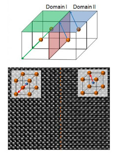
Caption: Bismuth ferrite is an insulator, but different domains may have different electrical polarizations. The position of the central iron atom and the displacement of the bismuth atoms in each cubic cell determine the polarization of the domain. In this transmission electron image, structural changes appear near and inside the wall. As a consequence, the domain walls themselves (along dotted line), which are just two nanometers wide, can conduct electricity at room temperature.

Credit: Lawrence Berkeley National Laboratoy, UC Berkeley. Usage Restrictions: with credit as above
Jan Seidel of the UC Department of Physics came upon the unique domain-wall properties of bismuth ferrite as he was performing scanning-probe measurements on thin films of the material created by Lane Martin of MSD; both are members of the Quantum Materials program.

"To make the films we hit targets of ceramic oxides containing bismuth and iron with a laser pulse and convert the solid to a plasma plume that is deposited on the substrate," Martin explains. "We choose the substrate structure and control the temperature and atmosphere to get the right mix and the right phase."

For the present work Martin grew films of bismuth ferrite between 50 and 200 nanometers thick on substrates of strontium titanium oxide (SrTiO3), a crystal whose similar lattice parameters and structure encouraged the growth of high-quality bismuth ferrite films. (A thin layer of a different compound, strontium ruthenium oxide (SrRuO3), was first laid down between the substrate and the bismuth ferrite to serve as an electrode.)

Like many other multiferroic oxides, bismuth ferrite has the crystal structure of perovskite, in which planes of oxygen atoms and heavy atoms (like bismuth) alternate with planes of oxygen atoms and lighter atoms (like iron). An iron atom is at the center of the basic bismuth ferrite cubic cell, and its position – whether slightly off center in one direction or another – plus the positions of affected bismuth atoms, gives rise to local polarization.

The bismuth ferrite films contained ferroelectric domains between 5 and 10 micrometers (millionths of a meter) in dimension, and, says Seidel, "we can map and even change the domain structure by using different scanning-probe mechanisms."

Bismuth ferrite is an insulator, but each domain has a distinct polarization or orientation of charge, which Seidel mapped using a piezoresponse force microscope (PFM): as the PFM probe moves across a sample, an alternating electric field in the tip gives rise to a detectable mechanical response in the sample, according to its polarization. The same PFM setup can control the nature of the local polarization of the film by applying a large enough voltage to switch it.

To map out the topographic features of the film surface, the scanning probe was used in atomic force microscopy (AFM) mode. In AFM the probe effectively "feels" its way across the surface, like a stylus in a record player feeling the grooves in a record. Moreover, by setting a voltage that is too slight to affect the polarization of the domains, the researchers can probe the electronic properties of the films.

In this mode (conducting AFM), Seidel measured the local conductivity of the sample across the domains and across domain walls. The domains were indeed nonconducting – since bismuth ferrite is an insulator – but surprisingly, certain domain walls exhibited electrical conductivity. Their conductivity depended on the angular difference in the direction of the polarization on either side of the domain wall.

To understand this unexpected conductivity, the researchers used transmission electron microscopy (TEM) at Berkeley Lab's National Center for Electron Microscopy, a national user facility supported by BES, to inspect how the atoms were differently arranged, in the domains and near the domain walls. Bismuth ferrite's domain walls are oriented along two distinct crystallographic planes; they can separate domains with either 109-degree, 71-degree, or 180-degree differences in the direction of polarization. By comparing the atomic structure of a nonconducting 71-degree domain wall to the atomic structure of a conducting 109-degree domain wall, the researchers found a clear difference in local structure: it promised to hold the key to understanding the origin of the effect.

How an insulating material's domain walls can conduct electricity

"We worked with theorists to help us model the behavior we had observed and to understand the mechanism of the conduction," says Ramesh. "What emerged was a clear picture of the changes in the structure of the unit cells of the bismuth ferrite near the domain walls." These structural changes are directly connected to a local change in the electronic properties of the material at the center of the domain wall.

"What happens is that as the positions of the central iron atoms change crossing the domain wall, the polarization increases perpendicular to the domain wall – but at the same time goes to zero parallel to the wall, before increasing again," says Martin. "This causes any free electrons in the vicinity to accumulate at the wall, where they can move along the wall itself."

The researchers' calculations also showed that the band gap of bismuth ferrite – a critical property for determining the electronic properties of materials used in electronic devices – decreased markedly in the center of the 109-degree and 180-degree domain walls, consistent with the increase in conductivity there. But in nonconducting 71-degree domain walls, the band gap decreased much less.

What strikes Seidel about these results "is the fundamental science. We have found a basic property of ferroelectric materials, and of ferroelectricity itself, that was not known before. Ferroelectrics have been studied for over half a century, but this is the first observation of this type of conduction."

Martin is enthusiastic about the potential applications of their discovery. "Domain walls may be the ultimate nanoscale feature," he says. "They're intrinsic to the material – they want to be there. And they're only two nanometers wide! It's like shoving a graphene sheet" – a single layer of carbon atoms with remarkable conductive properties – "right down into a tough, insulating ceramic."

For Ramesh, the discovery, in an oxide, of domain walls that conduct electricity like a metal is a step along "the path to the Holy Grail of oxide materials, the challenge of creating and controlling metal-insulator transitions at interfaces in a material. It's why DOE is so interested in this kind of research." ###

"Conduction at domain walls in oxide multiferroics," by Jan Seidel, Lane Martin, Qing He, Qian Zhan, Ying-Hao Chu, Axel Rother, Michael Hawkridge, Petro Maksymovych, Pu Yu, Marcin Gajek, Nina Balke, Sergei Kalinin, Sibylle Gemming, Feng Wang, Gustau Catalan, James Scott, Nicola Spaldin, Joseph Orenstein, and Ramamoorthy Ramesh, appears in the January 25, 2009 issue of the journal Nature Materials.

In addition to Seidel, Martin, and Ramesh, the team includes researchers from Berkeley Lab and UC Berkeley; the National Chiao Tung University, Taiwan; the Technische Universitat and the Forschungzentrum Dresden-Rossendorf in Dresden, Germany; Oak Ridge National Laboratory; the University of Cambridge, England; and UC Santa Barbara. Advanced Online Publication of the article in Nature Materials is at www.nature.com/nmat/journal/.

Berkeley Lab is a U.S. Department of Energy national laboratory located in Berkeley, California. It conducts unclassified scientific research and is managed by the University of California. Visit our website at http://www.lbl.gov.

Saturday, March 07, 2009

Smallest ever quantum dots bring real world applications closer VIDEO

Single atom quantum dots created by researchers at Canada's National Institute for Nanotechnology and the University of Alberta make possible a new level of control over individual electrons, a development that suddenly brings quantum dot-based devices within reach. Composed of a single atom of silicon and measuring less than one nanometre in diameter, these are the smallest quantum dots ever created.

Quantum dots have extraordinary electronic properties, like the ability to bottle-up normally slippery and speedy electrons, that allow controlled interactions among electrons to be put to use to do computations. Until now, quantum dots have been useable only at impractically low temperatures, but the new atom-sized quantum dots perform at room temperature.


Caption: An animation explaining the use of single atom quantum dots to enable the QCA computation scheme.

Credit: Robert A. Wolkow. Usage Restrictions: The video may only be used with the caption/credit provided.
Often referred to as artificial atoms, quantum dots have previously ranged in size from 2-10 nanometers in diameter. While typically composed of several thousand atoms, all the atoms pool their electrons to "sing with one voice", that is, the electrons are shared and coordinated as if there is only one atomic nucleus at the centre. That property enables numerous revolutionary schemes for electronic devices.

Research project leader Robert A. Wolkow described the potential impact saying, "Because they operate at room temperature and exist on the familiar silicon crystals used today's computers,
we expect these single atom quantum dots will transform theoretical plans into real devices."
Atomic Quantum Dot QCA Cell 1

Caption: Four atomic quantum dots are coupled to form a "cell" for containing electrons. The cell is filled with just two electrons. Control charges are placed along a diagonal to direct the two electrons to reside at just two of the four quantum dots comprising the cell. This new level of control of electrons points to new computation schemes that require extremely low power to operate. Such a device is expected to require about 1,000 times less power and will be about 1,000 times smaller than today's transistors.

Credit: Robert A. Wolkow. Usage Restrictions: Image can only be used with caption/photo credit provided.
The single atom quantum dots have also demonstrated another advantage – significant control over individual electrons by using very little energy. Wolkow sees this low energy control as the key to quantum dot application in entirely new forms of silicon-based electronic devices, such as ultra low power computers. "The capacity to compose these quantum dots on silicon, the most established electronic material, and to achieve control over electron placement among dots at room temperature puts new kinds of extremely low energy computation devices within reach." ###

The single atom quantum dots and their ability to control electrons is the focus of a paper titled "Controlled Coupling and Occupation of Silicon Atomic Quantum Dots at Room Temperature" posted January 27, 2009 in the on-line edition and published in the January 30, 2009, edition of Physical Review Letters.
Contact: Shannon Jones Shannon.Jones@nrc-cnrc.gc.ca 780-641-1626 University of Alberta

Friday, March 06, 2009

UT to develop fracture putty for traumatic leg injuries

Biomedical engineers at The University of Texas Health Science Center at Houston are leading a multi-institution initiative to produce a bio-compatible compound designed to mend serious leg fractures.

The researchers have been awarded $5.2 million in initial funding from the U.S. Department of Defense to develop "fracture putty" that could be used to regenerate bones shattered by roadside bombs or other explosive devices. This type of injury is called a non-union fracture and generally will not heal in a timely manner. It can lead to amputation. The total value of the effort, if all phases of the development program are completed, could be up to $7.9 million.

Serious leg injuries typically are repaired with bone grafts. Pins, plates or screws hold the grafts to healthy bone and external fixators provide support. Soldiers may require multiple surgeries and recuperation periods of about a year. And, they may not recoup full use of the injured leg.

Fracture putty for traumatic bone regeneration

Panel 1: The fracture putty (or BioNanoScaffold) composite material is implanted in the site of the shattered bone. Growth factors are released from the implant and recruit the patient's cells. The putty is load-bearing, so the patient is able to walk while the bone heals.

Fracture putty for traumatic bone regeneration

Panel 2: The fracture putty is infiltrated by cells which begin to create new bone. At the same time, the material constituting the fracture putty, starts degrading.

Fracture putty for traumatic bone regeneration

Panel 4: Several months after injury, the architecture and function of the bone are fundamentally restored.
If fracture putty proves successful, injured soldiers could fundamentally regain full use of their legs in a much shorter period of time. It could also be used in emergency rooms to treat civilians injured in traffic accidents and other traumatic events, said Mauro Ferrari, Ph.D., principal investigator and deputy chairman of the Department of Biomedical Engineering, a joint venture among the UT Health Science Center at Houston, The University of Texas at Austin and The University of Texas M. D. Anderson Cancer Center.

"Success on even a small part of the project has the potential to revolutionize orthopedic medicine. It could give people with serious leg injuries an opportunity to regain full use of limbs that now require amputations or the use of permanent implants," Ferrari said. "We're creating a living material that can be applied to crushed bones. The putty will solidify inside the body and provide support while the new bone grows."

"Anything you can do to start the healing process as quickly as possible is good for the patient," said John Holcomb, M.D., a retired U.S. Army Surgeon who now heads the Center for Translational Injury Research at the UT Health Science Center at Houston. "This could reduce the risk of infection and the onset of complications."

The DOD agency funding the project, the Defense Advanced Research Projects Agency (DARPA), sponsors revolutionary high-risk, high-payoff research that bridges the gap between fundamental discoveries and their military and civilian use. DARPA Program Manager Mitchell Zakin, Ph.D., said: "This undertaking represents the ultimate convergence of materials science, mechanics and orthopedics. I look forward to the first results, which should present themselves in about a year or so."
Ennio Tasciotti, Ph.D., a research assistant professor in Ferrari's lab, said the putty will include a material called nanoporous silicon that was developed in Ferrari's lab, which will give the putty the strength it needs to support the patient's weight while new bone tissue is being regenerated.

Developing a new way to repair long bone injuries is extremely challenging. According to Tasciotti, "This problem will require the contributions of a team of the best scientists in the fields of nanoporous silicon, bio-mimetic peptides, bio-polymers, stem cells and adhesives. The solution will come from the integration of nanomaterials with unique properties in a smart composite substance that can mimic bone structure and function."

He added, "The fracture putty will serve as a bioactive scaffold and will be able to substitute for the damaged bone. At the same time, the putty will facilitate the formation of natural bone and self-healing in the surrounding soft tissue through the attraction of the patient's own stem cells. The putty will have the texture of modeling clay so that it can be molded in any shape in order to be used in many different surgical applications including the reconnection of separated bones and the replacement of missing bones."

Tasciotti said the fracture putty could one day be used to address injuries involving the spine, skull and facial bones. "The findings of this research could eventually benefit all the victims of any bone-related traumatic injury and reduce the number of wartime amputations in the military as well the civilian population," he said.

"The technology to be explored through this research presents the potential to revolutionize the treatment of bone fractures, both in civilian clinics and on the battlefield," said Rice University investigator Antonios Mikos, Ph.D., the J.W. Cox Professor in Bioengineering, professor of chemical and biomolecular engineering and the director of Rice's Center for Excellence in Tissue Engineering. He is collaborating on the project.

If the fracture putty works in an animal model, the next step would involve patients. "We have been in preliminary conversations with the U.S. Food and Drug Administration, and it appears that fracture putty may be classified as a combination product, with the primary mode of action being that of a drug," Ferrari said.

Ferrari's colleagues at the UT Health Science Center at Houston on the project include: Paul Simmons, Ph.D., director of the Centre for Stem Cell Research at the Brown Foundation Institute of Molecular Medicine for the Prevention of Human Diseases; Mark Wong, D.D.S., associate professor and chairman of the Department of Oral and Maxillofacial Surgery at the University of Texas Dental Branch at Houston and professor in the Division of Oral and Maxillofacial Surgery at The University of Texas Medical School at Houston; Nagi Demian, M.D., D.D.S., assistant professor at the UT Dental Branch; Paolo Decuzzi, Ph.D., associate professor of health informatics at The University of Texas School of Health Information Sciences at Houston; and Milos Kojic, Ph.D., visiting professor of health informatics at UT School of Health Information Sciences and senior research scientist in the Department of Environmental Health at Harvard School of Public Health. ###

Also collaborating on the project are: George Whitesides, Ph.D., 1998 recipient of the National Medal of Science and the Woodford L. and Ann A. Flowers University Professor at Harvard University; Samuel Stupp, Ph.D., director of the Institute for BioNanotechnology in Medicine at Northwestern University; Bradley Weiner, M.D., orthopaedic surgery at The Methodist Hospital; Philip Noble, Ph.D., professor of orthopedic surgery at the Baylor College of Medicine; and two faculty members from Texas A & M University: Raffaella Righetti, Ph.D., assistant professor in the Dwight Look College of Engineering, and Theresa Fossum, D.V.M., Ph.D., professor and the Tom & Joan Read Chair in Veterinary Surgery in the College of Veterinary Medicine & Biomedical Sciences.

Ferrari serves as director of the nanomedicine division at the UT Health Science Center at Houston, professor of Experimental Therapeutics at the University of Texas M. D. Anderson Cancer Center, adjunct professor of bioengineering at Rice University, adjunct professor of biochemistry and molecular biology at The University of Texas Medical Branch at Galveston, president of the Alliance for NanoHealth, Houston, and adjunct professor of mathematics and mechanical engineering at the University of Houston.

Contact: Robert Cahill Robert.Cahill@uth.tmc.edu 713-500-3030 University of Texas Health Science Center at Houston