Friday, February 29, 2008

Credit-card-sized platform for volatile compound analysis CAREER project goal

Masoud Agah, Virginia Tech College of Engineering researcher

Caption: Masoud Agah, an assistant professor in the Bradley Department of Electrical and Computer Engineering and an affiliate member of the Department of Mechanical Engineering faculty at Virginia Tech, has received an NSF CAREER Award to support his research to develop a credit-card-sized gas chromatography platform that can analyze volatile compounds within seconds. Credit: Virginia Tech Photo. Usage Restrictions: with announcement of Dr. Agah's CAREER award
Blacksburg, Va. — Developing a credit-card-sized gas chromatography platform that can analyze volatile compounds within seconds is the next step for Virginia Tech College of Engineering researcher Masoud Agah, who has received a National Science Foundation (NSF) Faculty Early Career Development Program (CAREER) Award to support his research.

Agah, an assistant professor in the Bradley Department of Electrical and Computer Engineering and an affiliate member of the Department of Mechanical Engineering faculty, recently secured a five-year CAREER grant worth $400,000. This is the NSF’s most prestigious award for creative junior faculty who are considered to be future leaders in their academic fields.

Gas chromatography is the primary technique used in a number of scientific, medical, and industrial settings to separate and analyze volatile compounds in gases, liquids, and solids.

Medical researchers, for example, can isolate volatile organic compounds in breath samples for early diagnosis or evaluation of certain metabolic conditions and diseases. Acetone in a patient’s breath can be a marker for diabetes, Agah said, and scientists have identified a group of compounds that appear to be markers for breast cancer.

Gas chromatography is used in the field of environmental monitoring to identify certain air pollutants and drinking water and groundwater contaminants.
Homeland security and military personnel can rely on the technique to test air samples for chemical warfare agents, such as sarin and mustard gases. The technique also is widely used in food processing, the petrochemical industry, and a number of other fields.

Currently, gas chromatography systems consist of a gas tank, sample injector, separation column, and gas detector. Samples to be analyzed are vaporized and injected into the column, where compounds are separated and then passed over the detector. Conventional systems tend to be large, fragile, and relatively expensive table-top instruments.

Agah, who established the Microelectromechanical Systems (MEMS) Laboratory (www.ece.vt.edu/mems/) at Virginia Tech shortly after joining the university in 2005, is attempting to develop a gas chromatographic architecture that will fit on a platform the size of a credit card and will separate and analyze a complex range of compounds in only a few seconds.

To create this new architecture, which he has named “GC Matrix,” Agah is employing MEMS technology. In his laboratory, he is developing gas chromatographic columns with heaters, temperature sensors, pressure sensors, and thermal conductivity detectors that can fit on micro-chips. Agah already has developed columns that can separate a limited number of volatile compounds and chemical warfare agent simulants in less than 10 seconds.

In addition to significantly improving the speed, portability, and performance, Agah’s GC Matrix will consume far less power than conventional instruments.

Once perfected, the GC Matrix could be used in a number of industrial and scientific applications. The apparatus also could be effective in saving lives during crises. Emergency workers, for instance, could easily carry GC Matrix instruments into areas devastated by floods to test water for toxic chemicals, and soldiers on the battlefield could test the air within seconds for signs of chemical warfare agents.

Every CAREER award project includes an educational component. Agah will develop a new university laboratory course on MEMS technology. He also is working with Virginia Tech’s National Society of Black Engineers and the Institute of Electrical and Electronics Engineers’ Teacher in Service Program to establish the High-School Microsystems Engineering Program. ###

Before joining the Virginia Tech faculty in 2005, Agah conducted research at the NSF Center for Wireless Integrated MicroSystems at the University of Michigan-Ann Arbor, where he developed MEMS-based gas chromatography columns for environmental monitoring applications. He completed his Ph.D. in electrical engineering at Michigan and received his B.S. and M.S. degrees from Sharif University of Technology in Iran.

Contact: Liz Crumbley lcrumb@vte.du 540-231-9772 Virginia Tech

Tags: or and or and or

Thursday, February 28, 2008

MIT creates gecko-inspired bandage

MIT Institute Professor Robert Langer and faculty member Jeffrey Karp

MIT Institute Professor Robert Langer and faculty member Jeffrey Karp, both affiliated with the Harvard-MIT Division of Health Sciences and Technology, display an adhesive they developed that was inspired by the gecko and may have medical and surgical applications. Photo / Donna Coveney
MIT researchers and colleagues have created a waterproof adhesive bandage inspired by gecko lizards that may soon join sutures and staples as a basic operating room tool for patching up surgical wounds or internal injuries.

Drawing on some of the principles that make gecko feet unique, the surface of the bandage has the same kind of nanoscale hills and valleys that allow the lizards to cling to walls and ceilings. Layered over this landscape is a thin coating of glue that helps the bandage stick in wet environments, such as to heart, bladder or lung tissue. And because the bandage is biodegradable, it dissolves over time and does not have to be removed.
The team is led by MIT Institute Professor Robert Langer and Jeff Karp, an instructor of medicine at Brigham and Women's Hospital and Harvard Medical School. Both are also faculty members at the Harvard-MIT Division of Health Sciences and Technology (HST). Their colleagues include several other researchers from MIT, as well as from the University of Basel, Switzerland. In addition, Dr. Jeff Borenstein and David J. D. Carter from Draper Laboratory fabricated the nanomolds involved in the work, and Jay Vacanti and Cathryn Sundback performed all animal experiments with colleagues at Massachusetts General Hospital.
foot of a Tokay gecko

This foot of a Tokay gecko shows its adhesive pads. The gecko, whose feet enable it to cling tightly while upside down or on vertical surfaces, helped inspire a new medical bandage created by an MIT-led research team. Photo / David Clements, via Wikimedia
The work is described in the Feb. 11 online issue of the Proceedings of the National Academy of Sciences.

"There is a big need for a tape-based medical adhesive," said Karp. For instance, a surgical adhesive tape made from this new material could wrap around and reseal the intestine after the removal of a diseased segment or after a gastric bypass procedure. It could also patch a hole caused by an ulcer. Because it can be folded and unfolded, it has a potential application in minimally invasive surgical procedures that are particularly difficult to suture because they are performed through a very small incision.

Gecko-like dry adhesives have been around since about 2001 but there have been significant challenges to adapt this technology for medical applications given the strict design criteria required. For use in the body, they must be adapted to stick in a wet environment and be constructed from materials customized for medical applications. Such materials must be biocompatible, meaning they do not cause inflammation; biodegradable,
meaning they dissolve over time without producing toxins; and elastic, so that they can conform to and stretch with the body's tissues.

The MIT researchers met these requirements by building their medical adhesive with a "biorubber" invented by Karp, Langer and others. Using micropatterning technology--the same technology used to create computer chips--the researchers shaped the biorubber into different hill and valley profiles at nanoscale dimensions. After testing them on intestinal tissue taken from pigs, they selected the stickiest profile, one with pillars spaced just wide enough to grip and interlock with the underlying tissue.
MIT's gecko-inspired medical adhesive

MIT's gecko-inspired medical adhesive consists of a "biorubber" base patterned to have pillars that are less than a micrometer in diameter and three micrometers in height. Layered on top is a thin coating of a sugar-based glue. Tests in live rats suggest that the adhesive could be an effective operating room tool for closing surgical wounds. Graphic courtesy / Edwin Chan and David Carter
Karp then added a very thin layer of a sugar-based glue, to create a strong bond even to a wet surface. The resulting bandage "is something we never expect to remove," said Karp. Because of that difference, he continued, "we're not mimicking the gecko"--which has sticky feet but can still lift them up to walk--"we are inspired by the gecko to create a patterned interface to enhance the surface area of contact and thus the overall strength of adhesion."

When tested against the intestinal tissue samples from pigs, the nanopatterned adhesive bonds were twice as strong as unpatterned adhesives. In tests of the new adhesive in living rats, the glue-coated nanopatterned adhesive showed over a 100 percent increase in adhesive strength compared to the same material without the glue. Moreover, the rats showed only a mild inflammatory response to the adhesive, a minor reaction that does not need to be overcome for clinical use.

Among other advantages, the adhesive could be infused with drugs designed to release as the biorubber degrades.
Further, the elasticity and degradation rate of the biorubber are tunable, as is the pillared landscape. This means that the new adhesives can be customized to have the right elasticity, resilience and grip for different medical applications.

"This is an exciting example of how nanostructures can be controlled, and in so doing, used to create a new family of adhesives," said Langer.

Other MIT authors of the paper are co-first authors Alborz Mahdavi, a former MIT lab technician now at the California Institute of Technology; Lino Ferreira, a former MIT postdoctoral fellow now at the University of Coimbra, Portugal; Jason W. Nichol and Edwin P. Chan, HST postdoctoral fellows; HST doctoral student Chris Bettinger; and MIT graduate students Siamrut Patanavanich, Loice Chignozha, Eli B. Joseph, Alex Galakatos and Seungpyo Hong, all from the Department of Chemical Engineering.

The work was funded by the National Institutes of Health, the Materials Research Science and Engineering Center (MRSEC) program of the National Science Foundation, and the MIT-Portugal program.

Contact: Elizabeth Thomson thomson@mit.edu 617-258-5402 Massachusetts Institute of Technology Elizabeth Dougherty, Harvard-MIT Division of Health Sciences and Technology

Wednesday, February 27, 2008

Nanotech's health, environmental impacts worry scientists and the public

Elizabeth A. Corley

Elizabeth A. Corley is Assistant Professor in the School of Public Affairs at Arizona State University. Elizabeth’s research interests focus on science policy and environmental policy.
BOSTON – Scientists and the public agree that the promise of nanotechnology is great, but there are risks to it and they should be governed accordingly.

The new technology, which is making its way into products ranging from food storage containers to computers, is seen differently among scientists than the general public, with scientists appearing to be more concerned in some areas. But in broad categories of risk versus reward both groups seem to agree – go slow and be cautious of the technology’s deleterious effects. What may be most useful in the future are good, trusted communicators.

These are among the findings of a recent survey that will be presented by Elizabeth Corley, an Arizona State University assistant professor in the School of Public Affairs, on Feb. 15 at the American Association for the Advancement of Science annual meeting. The report is based on a national telephone survey of American households and a sampling of 363 leading U.S. nanotechnology scientists and engineers.
It reveals that scientists who have the most insight into a technology with enormous potential -- and that is already emerging in hundreds of products -- are unsure what health and environmental problems might be posed by the technology.

Findings of the report, first published in the journal Nature Nanotechnology (Nov. 25, 2007), were in stark contrast to controversies sparked by the advent of major past technologies, such as nuclear power and genetically modified foods, which scientists perceived as having lower risks than did the public.

Nanotechnology is based on science’s newfound ability to manipulate matter at the smallest scale, on the order of molecules and atoms. The field has enormous potential to develop applications ranging from new antimicrobial materials and tiny probes to sample individual cells in human patients, to vastly more powerful computers and lasers. Already, products with nanotechnology built in include golf clubs, tennis rackets and antimicrobial food storage containers.

At the root of the information disconnect, said Corley, who conducted the survey with Dietram Scheufele of the University of Wisconsin-Madison, is that nanotechnology is only now starting to emerge on the nation’s policy agenda. Amplifying the problem is that the news media have not paid much attention to nanotechnology and its implications.

“In the long run, this information disconnect could undermine public support for federal funding in certain areas of nanotechnology research, particularly in those areas that the public views as having lower levels of risk,” Corley said.

While scientists were generally optimistic about the potential benefits of nanotechnology, they expressed significantly more concern about pollution and new health problems related to the technology. Twenty percent of the scientists responding to the survey indicated a concern that new forms of nanotechnology pollution may emerge, while only 15 percent of the public thought that might be a problem. More than 30 percent of scientists expressed concern that human health may be at risk from the technology, while just 20 percent of the public held such fears.

Of more concern to the American public, according to the report, are a potential loss of privacy from tiny new surveillance devices and the loss of more U.S jobs. Those fears were less of a concern for scientists.

While divergent in some specific views, Corley said that scientists and the public seem to agree in broad terms on the rewards versus the risks of nanotech.

“Not surprisingly, scientists are more likely than the public to find nanotechnology research useful and morally acceptable,” Corley said. “Yet, scientists and the public have similar perceptions (around 17 percent) of the overall risks of nanotechnology and the need for government regulations of nanotechnology (around 40 percent).

“Our new analysis shows that despite scientists’ perceptions of high levels of benefit from nanotechnology research, they tend to agree with the public that they should pay attention to government regulations and unknown risks,” she explained.

Corley added that the survey shows university scientists are the ones thought to be most qualified to communicate the potential risks and benefits of the technology. Some 88 percent of scientists believe university scientists have the necessary expertise, while about 75 percent think that nanotech industry scientists have the required level of expertise. Yet the public is less likely to trust nanotech industry scientists. Of the three groups that the public trusts most -- university scientists, consumer organizations and regulators – the only group that more than half the public trusts are university scientists.

“This is a policy relevant finding,” she added, “because, on average, university nanotech scientists have been hesitant to engage the public in this sort of discourse.” ###

Contact: Skip Derra skip.derra@asu.edu 480-965-4823 Arizona State University Source: Elizabeth Corley, (602) 496-0462; elizabeth.corley@asu.edu

Tags: or and or and or

Tuesday, February 26, 2008

Protein's strength lies in H-bond cooperation VIDEO


The video shows the failure of a beta-sheet model system under shear loading. As the middle strand is pulled with a constant speed, the rupture of hydrogen bonds in clusters leads to failure of the beta-sheet assembly. VIDEO / SINAN KETEN

Geometric confinement in clusters enhances robustness of materials like spider silk
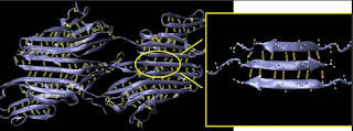
beta-sheet protein, Z1-Z2 telethonin complex

This figure shows the structure of a beta-sheet protein, Z1-Z2 telethonin complex, in the giant muscle protein titin. The inset shows the orientation of the protein backbone of three beta strands (in purple) with hydrogen bonds (yellow) holding the assembly together. Buehler and Keten found that hydrogen bonds in beta-sheet structures break in clusters of three or four, even in the presence of many more bonds. IMAGE / SINAN KETEN and MARKUS BUEHLER
CAMBRIDGE, Mass. — Researchers in Civil and Environmental Engineering at MIT reveal that the strength of a biological material like spider silk lies in the specific geometric configuration of structural proteins, which have small clusters of weak hydrogen bonds that work cooperatively to resist force and dissipate energy.

This structure makes the lightweight natural material as strong as steel, even though the “glue” of hydrogen bonds that hold spider silk together at the molecular level is 100 to 1,000 times weaker than the powerful glue of steel’s metallic bonds or even Kevlar’s covalent bonds.
Based on theoretical modeling and large-scale atomistic simulation implemented on supercomputers, this new understanding of exactly how a protein’s configuration enhances a material’s strength could help engineers create new materials that mimic spider silk’s lightweight robustness. It could also impact research on muscle tissue and amyloid fibers found in brain tissue.

“Our hope is that by understanding the mechanics of materials at the atomistic level, we will be able to one day create a guiding principle that will direct the synthesis of new materials,” said Professor Markus Buehler, lead researcher on the work.

In a paper published in the Feb. 13 online issue of Nano Letters, Buehler and graduate student Sinan Keten describe how they used atomistic modeling to demonstrate that the clusters of three or four hydrogen bonds that bind together stacks of short beta strands in a structural protein rupture simultaneously rather than sequentially when placed under mechanical stress. This allows the protein to withstand more force than if its beta strands had only one or two bonds. Oddly enough, the small clusters also withstand more energy than longer beta strands with many hydrogen bonds.

“Using only one or two hydrogen bonds in building a protein provides no or very little mechanical resistance, because the bonds are very weak and break almost without provocation,” said Buehler, the Esther and Harold E. Edgerton Assistant Professor in the Department of Civil and Environmental Engineering. “But using three or four bonds leads to a resistance that actually exceeds that of many metals. Using more than four bonds leads to a much-reduced resistance. The strength is maximized at three or four bonds.”

After observing the simultaneous rupture of these hydrogen-bond clusters within the proteins in their atomistic simulations, Buehler and Keten wanted to know why the bonds break in small clusters, even in long strands with many hydrogen bonds. They used the laws of thermodynamics to explain this phenomenon. The paper in Nano Letters describes how the external force changes the entropic energy in the system and leads to the rupture of hydrogen bonds. By calculating the energy necessary to initiate the unfolding process in a protein molecule, they demonstrated that adding more hydrogen bonds in longer strands would not increase the material’s strength.

“You would simply have this long chain of beta strands with lazy bonds that don’t contribute to the strength of the assembly,” said Keten. “But a material that employs many short beta strands folded and connected by three or four hydrogen bonds may exhibit strength greater than steel. In metals, the energy would be stored directly in much stronger bonds, called metallic bonds, until bonds rupture one by one. In proteins, things are more complicated due to the entropic elasticity of the noodle-like chains and the cooperative nature of the hydrogen bonds.”

Structural proteins contain a preponderance of beta-sheets, sections that fold in such a way that they look a bit like old-fashioned ribbon candy; short waves or strands appear to be stacked on top of one another, each just the right length to allow three or four hydrogen bonds to connect it to the section above and beneath.

Beta sheets with short strand lengths connected by three or four hydrogen bonds are the most common conformation among all beta-structured proteins, including those comprising muscle tissue, according to experimental proteomics data on protein structures in the Protein Data Bank.

This correlation of a common geometric configuration among beta sheets—which are one of the two most prevalent protein structures in existence—suggests that a protein’s strength is an important evolutionary driving force behind its physical design. The researchers observed the same behavior in similar small clusters in alpha-helical structural proteins, the other most prevalent protein, but haven’t yet studied those assemblies in detail.

On the other hand, synthetic materials like steel have a very different and crystalline structure held together by the stronger glue of metallic bonds. Because steel and other synthetic materials tend to be dense, and therefore heavy, they consume a good deal of energy in manufacturing and transport.

“Metals are configured with bonds that are much stronger and require a much greater force to break,” said Buehler. “However, the crystalline lattice of a metal’s structure is never perfect; it contains defects that effectively reduce the material’s strength quite drastically. When you place a load on the metal, the defect can fail, possibly causing a crack to propagate. In protein’s beta sheets, the confined nature of the hydrogen bond clusters helps to dissipate the energy without compromising the strength of the material. This shows the amazing ingenuity and efficiency of natural materials.”

This research was supported by an MIT Presidential Graduate Fellowship, the Army Research Office, a National Science Foundation CAREER Award, the Solomon Buchsbaum AT&T Research Fund, and a grant from the San Diego Supercomputing Center (SDSC).

By Denise Brehm Civil & Environmental Engineering. Contact: Denise Brehm brehm@mit.edu 617-253-8069 Massachusetts Institute of Technology, Department of Civil and Environmental Engineering

Tags: or and or and or

Monday, February 25, 2008

Strategy for nanotechnology-related environmental, health and safety research

NSET Releases Document: Strategy for Nanotechnology-Related Environmental, Health, and Safety Research

Strategy for Nanotechnology-Related Environmental, Health, and Safety ResearchThe Nanoscale Science, Engineering, and Technology (NSET) Subcommittee of the National Science and Technology Council's Committee on Technology today released a document
describing the National Nanotechnology Initiative’s (NNI) strategy for addressing priority research on the environmental, health, and safety (EHS) aspects of nanomaterials

Strategy for Nanotechnology-Related Environmental, Health, and Safety Research was prepared by the subcommittee’s Nanotechnology Environmental and Health Implications (NEHI) Working Group. The full report is available for download in PDF format.

EHS research and information needs related to nanotechnology were identified in the NSET Subcommittee documents Environmental, Health, and Safety Research Needs for Engineered Nanoscale Materials, (PDF) published in September 2006 and Prioritization of Environmental, Health, and Safety Research Needs for Engineered Nanoscale Materials: An Interim Document for Public Comment, (PDF) released in August 2007.

Strategy for Nanotechnology-Related Environmental, Health, and Safety Research presents a path for coordinated interagency implementation of research to address the needs identified in earlier reports. It is based in part on a detailed analysis of the Federal Government's FY 2006 nanotechnology-related EHS research portfolio, a $68 million investment in 246 projects. Experts from the NEHI Working Group analyzed how these activities addressed the priority research needs and then proposed emphasis and sequencing for future research efforts. Agency-specific research and regulatory needs, public comments on the prior documents, and considerations of the state of EHS research in the national and international nanotechnology communities all played an important role in shaping the strategy.

“This EHS research strategy is the result of a terrific team effort led by the NEHI Working Group. It reflects a strong consensus and commitment among the NNI member agencies on the roles they will assume, consistent with their respective missions and responsibilities, to move the Federal efforts in nanotechnology-related EHS research forward. The quality of the document demonstrates that the NNI is working hard to understand—and to think strategically about—nano EHS issues in a systematic, coordinated fashion,” said Dr. Clayton Teague, Director of the National Nanotechnology Coordination Office.

About the National Science and Technology Council and the Nanoscale Science, Engineering, and Technology Subcommittee. The Federal Government's nanotechnology research programs, in general, fall under the National Nanotechnology Initiative (NNI). Coordination of research in the field takes place through the Nanoscale Science, Engineering, and Technology (NSET) Subcommittee of the National Science and Technology Council. The National Nanotechnology Coordination Office provides technical and administrative support to the NSET Subcommittee and serves as a central point of contact for the NNI.

Contact: Audrey Haar ahaar@nnco.nano.gov 443-257-8878 National Nanotechnology Coordination Office

Tags: or and or and or

Sunday, February 24, 2008

National Nanotechnology Initiative releases its fiscal year 2009 budget and highlights

Big Things from a Tiny WorldBudget and highlights to accompany the president's 2009 budget

February 14, 2008, 10 a.m.—A summary of the National Nanotechnology Initiative (NNI) Fiscal Year 2009 Budget was released today by the Nanoscale Science, Engineering, and Technology (NSET) Subcommittee of the National Science and Technology Council's Committee on Technology. The report is a supplement to the President’s Budget for Fiscal Year 2009, providing additional details on the NNI budget request, as well as highlights of planned activities to be conducted under that budget.
Described in the report are the programs and activities taking place across all 25 of the Federal agencies participating in the NNI. The document is available online from the home page of the NNI Web site (www.nano.gov) or directly at nano.gov/budget_summary. In PDF format.

The 2009 budget request provides $1.5 billion for the NNI, reflecting steady growth in the NNI investment. This sustained major investment in nanotechnology research and development (R&D) across the Federal Government over the past nine fiscal years of the NNI reflects the broad support of the Administration and of Congress for this program.

The NNI remains focused on fulfilling the Federal role of supporting basic research, infrastructure development, and technology transfer, in the expectation that the resulting advances and capabilities will make important contributions to national priorities, with applications across a wide range of industries including healthcare, electronics, aeronautics and energy. Increasing investments by mission agencies in nanotechnology-related research since 2001 reflect a recognition of the potential for nanotechnology research to support agency missions and responsibilities.

Key points from the report:

* The 2009 NNI budget provides increased support for research on fundamental nanoscale phenomena and processes, from $481 million in 2007 to $551 million in 2009.

* The proposed budget reflects substantial ongoing growth in funding for instrumentation research, metrology and standards (from $53 million in 2007 to $82 million in 2009) and in nanomanufacturing research (from $48 million in 2007 to $62 million in 2009).

* Environmental, Health, and Safety (EHS) R&D funding in 2009 ($76 million) is more than double the level of actual funding in 2005 ($35 million)—the first year this data was collected. The steady growth in EHS R&D spending follows the NNI strategy of expanding the capacity to do high-quality research in this field. ###

About the National Science and Technology Council and the Nanoscale Science, Engineering, and Technology Subcommittee. The Federal Government’s nanotechnology research programs, in general, fall under the National Nanotechnology Initiative (NNI). Coordination of research in the field takes place through the Nanoscale Science, Engineering, and Technology (NSET) Subcommittee of the National Science and Technology Council. The National Nanotechnology Coordination Office provides technical and administrative support to the NSET Subcommittee and serves as a central point of contact for the NNI.

Tags: or and or and or

Saturday, February 23, 2008

Remarkable new clothing may someday power your iPod

piezoelectric zinc oxide nanowires.

A scanning electron microscopy image shows the piezoelectric zinc oxide nanowires. The two sets of nanowires meet teeth-to-teeth, allowing the gold-coated microfibers to scrub those not coated with gold to produce electricity via a coupled piezoelectric-semiconducting process. This is the fundamental concept of a "power shirt."

Credit: Image courtesy of Z.L. Wang and X.D. Wang, Georgia Institute of Technology
The promise of piezoelectric fiber pairs, Nanotechnology researchers at the Georgia Institute of Technology are developing a shirt that harvests energy from the wearer's physical motion and converts it into electricity for powering small electronic devices worn by soldiers in the field, hikers and other users.

The research, funded by the National Science Foundation (NSF) and described in the Feb. 14 issue of Nature, details how pairs of textile fibers covered with zinc oxide nanowires generate electricity in response to applied mechanical stress. Known as "the piezoelectric effect," the resulting current flow from many fiber pairs woven into a shirt or jacket could allow the wearer's body movement to power a range of portable electronic devices.
The fibers could also be woven into curtains, tents or other structures to capture energy from wind motion, sound vibration or other mechanical energy.

"The two fibers scrub together just like two bottle brushes with their bristles touching, and the piezoelectric-semiconductor process converts the mechanical motion into electrical energy," Zhong Lin Wang, a Regents professor in the School of Materials Science and Engineering at the Georgia Institute of Technology. "Many of these devices could be put together to produce higher power output."

Zhong Lin Wang, Xudong Wang and Yong Qin

The Georgia Tech research team for fiber nanogenerators: (left to right) Zhong Lin Wang, Xudong Wang and Yong Qin.

Credit: Georgia Tech Photo: Gary Meek
Wang and collaborators Xudong Wang and Yong Qin have made more than 200 of the fiber nanogenerators. Each is tested on an apparatus that uses a spring and wheel to move one fiber against the other. The fibers are rubbed together for up to 30 minutes to test their durability and power production.

The researchers have measured current of about four nanoamperes and output voltage of about four millivolts from a nanogenerator that included two fibers that were each one centimeter long. With a much improved design,
Wang estimates that a square meter of fabric made from the special fibers could theoretically generate as much as 80 milliwatts of power.

So far, there is only one wrinkle in the fabric, so to speak - washing it. Zinc oxide is sensitive to moisture, so in real shirts or jackets, the nanowires would have to be protected from the effects of the washing machine. ###

The research was funded by NSF's Division of Materials Research through grant #0706436. "This multi-disciplinary research grant enables materials scientists and engineers from varied backgrounds to work together towards translating basic and applied research into viable technologies," said NSF Program Manager Harsh Deep Chopra. The research also was sponsored by the U.S. Department of Energy, and the Emory-Georgia Tech Nanotechnology Center for Personalized and Predictive Oncology.

Media Contacts: Diane Banegas, National Science Foundation (703) 292-4489 dbanegas@nsf.gov. John Toon, Georgia Institute of Technology (404) 894-6986 jtoon@gatech.edu

Program Contacts: Harsh D. Chopra, National Science Foundation (703) 292-4543 hchopra@nsf.gov

Principal Investigators: Zhong Lin Wang, Georgia Institute of Technology (404) 894-8008 zhong.wang@mse.gatech.edu

Related Websites: Professor Wang's Nano Research group:

Tags: or and or and or

Friday, February 22, 2008

Rice scientists make breakthrough in single-molecule sensing

Multimodal Sensors

Caption: Rice University scientists use tiny gaps between gold electrodes to simultaneously perform electronic and optical measurements of the same molecule. These scanning electron images show electrodes and gaps on a silicon chip. The color insets show optical signals due to the chip (top) and a gap (bottom). Credit: D. Natelson/Rice University. Usage Restrictions: Users must credit: D. Natelson/Rice University
Simultaneous optical and electronic measurements on same molecule

HOUSTON, -- In a study that could lay the foundation for mass-produced single-molecule sensors, physicists and engineers at Rice University have demonstrated a means of simultaneously making optical and electronic measurements of the same molecule.

The research, which is available online, is slated to appear in an upcoming issue of the journal Nano Letters. The experiments were performed on a nanoelectronic device consisting to two tiny electrodes separated by a molecule-sized gap. Using electric current, the researchers measured conduction through single molecules in the gap. In addition, light-focusing properties of the electrodes allowed the researchers to identify the molecule by a unique optical fingerprint.
"We can mass-produce these in known locations, and they have single-molecule sensitivity at room temperature in open air," said study co-author Douglas Natelson, associate professor of physics and astronomy and co-director of Rice's Quantum Magnetism Laboratory (QML). "In principle, we think the design may allow us to observe chemical reactions at the single-molecule level."

While scientists have used electronic and optical instruments to measure single molecules before, Rice's system is the first that allows both simultaneously -- a process known as "multimodal" sensing -- on a single small molecule.

The research sprang from a collaboration between Natelson's group -- where the electrodes were developed -- and Rice's Laboratory for Nanophotonics (LANP), where the simultaneous electronic and optical testing was performed. In research published last year, the two groups explained how the electrodes focus near-infrared light into the molecule-sized gap, increasing light intensity in the gap by as much as a million times. The increased intensity allows the team to collect unique optical signatures for molecules trapped there via a technique called surface enhanced Raman spectroscopy (SERS).

"Our latest results confirm that we have the sensitivity required to measure single molecules," said LANP Director Naomi Halas, the Stanley C. Moore Professor of Electrical and Computer Engineering and professor of chemistry. "That sensitivity, and the multimodal capabilities of this system, gives us a great tool for fundamental science at the nanoscale."

Daniel Ward, a student in Natelson's research group, built the electrodes from tiny gold wires on silicon wafers and performed the critical measurements. The group specializes in studying the electronic and magnetic properties of nanoscale objects -- particles and devices that are built with atomic precision. The devices are so small they can only be seen with certain types of microscopes, and even those provide unclear pictures at best. Natelson said the new multimodal device gives researchers a much clearer idea of what is going on by combining two different kinds of measurements, electronic and optical.

"Conduction across our electrodes is known to depend on a quantum effect called 'tunneling,'" Natelson said. "The gaps are so small that only one or two molecules contribute to the conduction. So when we get conduction, and we see the optical fingerprint associated with a particular molecule, and they track each other, then we know we're measuring a single molecule and we know what kind of molecule it is. We can even tell when it rotates and changes position." ###

Study co-authors include Jacob Ciszek, James Tour, Yanpeng Wu and Peter Nordlander, all of Rice. The research was sponsored by the National Science Foundation, the Welch Foundation, the Packard Foundation, the Sloan Foundation, the Research Corp., the Defense Advanced Research Projects Agency and the Air Force Office of Scientific Research.

Contact: Jade Boyd jadeboyd@rice.edu 713-348-6778 Rice University

Tags: or and or and or

Thursday, February 21, 2008

New funding to charge energy research at UCL and the London Centre for Nanotechnology

Hydrogen Storage Materials

Caption: A sample of a hydrogen storage material to be further prototyped in the new Wolfson-funded laboratories. The material is carbon-based and is already close to meeting some of the DoE targets for hydrogen storage. Credit: UCL/LCN. Usage Restrictions: None.
Professors Neal Skipper and Franco Cacialli, of the London Centre for Nanotechnology (LCN) and the Department of Physics & Astronomy, University College London (UCL), have been awarded a £200,000 laboratory refurbishment grant to help them develop alternative fuel supplies for transport and electricity generation. The Royal Society awarded the grant, with funding from the Wolfson Foundation under a scheme aiming to improve the UK’s research infrastructure.
The refurbishment programme will create a new facility to enable the team to address two important issues in carbon emission reduction: the creation of cheap, efficient storage for hydrogen, and the development of large-surface organic solar cells.

Professor Richard Catlow, Dean of the Faculty of Mathematics and Physical Sciences at UCL commented “This grant will greatly contribute to the search for alternative fuels and efficient renewable energy supplies, therefore building on UCL's strong programme of energy research. I am delighted to hear that the Royal Society and Wolfson Foundation are generously funding the laboratory refurbishment that will make this work possible.”

One of the more challenging problems in energy research is to find a compact, safe and lightweight alternative to petroleum that has similar energy densities. There are a large number of different potential solutions to this problem, but the use of hydrogen has interesting possibilities in that it promises a clean, efficient form of energy storage.

However, for the hydrogen economy to be practical there are a several technological challenges to be overcome, many of which are associated with the materials used to store the hydrogen itself. The required performance targets for the storage material have been compiled by the US Department of Energy (DoE). These targets include the amount of hydrogen that can be stored, how easily the material can be filled and emptied, its cost, lifetime and safety. At the moment there are various different technologies under investigation, but at the moment no material meets even the 2005 goals. The refurbished laboratory will allow the researchers to investigate some very promising nanostructured carbon-based materials which are non-toxic, recyclable and should meet the DoE’s targets.

The other key energy challenge to be tackled in the new laboratory is the efficient generation of electricity from solar energy. Professor Cacialli is developing solar cells on organic substrates that can be made over large surfaces. Unlike the glass-like traditional solar cells made from silicon, organic photovoltaics can be flexible, resembling plastic materials. Being flexible, they can easily be applied on uneven surfaces, e.g. it may be possible to wrap a building with energy-producing solar cells, effectively turning walls into generators. The new facilities will allow researchers to improve the nanoscale electronic components of solar cells leading to an increase in their efficiency and output.

Professors Skipper and Cacialli remarked "We were delighted to hear about the award, since this will enable us to carry out the laboratory refurbishments needed to intensify our efforts in the burgeoning areas of excitonic solar cells and hydrogen storage".

The refurbished laboratory will be located at the UCL Department of Physics and Astronomy, in central London. The project will complement both UCL’s and the LCN’s growing portfolio of energy research projects which total more than £10 million of investment. ###

Notes to editors: 1.About the London Centre for Nanotechnology. The London Centre for Nanotechnology is an interdisciplinary joint enterprise between University College London and Imperial College London. In bringing together world-class infrastructure and leading nanotechnology research activities, the Centre aims to attain the critical mass to compete with the best facilities abroad. Research programmes are aligned to three key areas, namely Planet Care, Healthcare and Information Technology and bridge together biomedical, physical and engineering sciences.
Website: www.london-nano.com

2.About University College London. Founded in 1826, UCL was the first English university established after Oxford and Cambridge, the first to admit students regardless of race, class, religion or gender, and the first to provide systematic teaching of law, architecture and medicine. In the government's most recent Research Assessment Exercise, 59 UCL departments achieved top ratings of 5* and 5, indicating research quality of international excellence.

UCL is in the top ten world universities in the 2007 THES-QS World University Rankings, and the fourth-ranked UK university in the 2007 league table of the top 500 world universities produced by the Shanghai Jiao Tong University. UCL alumni include Marie Stopes, Jonathan Dimbleby, Lord Woolf, Alexander Graham Bell, and members of the band Coldplay. Website: www.ucl.ac.uk

3. For information on the Royal Society Wolfson Laboratory Refurbishment Grant scheme

Contact: Dave Weston d.weston@ucl.ac.uk 44-020-767-97678 University College London

Tags: or and or and or

Wednesday, February 20, 2008

UA optical scientists add new, practical dimension to holography VIDEO


holographic Views of an automobile (top) and of a human brain (bottom)

Views of an automobile (top) and of a human brain (bottom), from the updatable 3D holographic display developed at The University of Arizona College of Optical Sciences in collaboration with Nitto Denko Technical Corp., Oceanside, Calif. The 3D images were recorded on a 4-inch by 4-inch photorefractive polymer device. (Credit: University of Arizona College of Optical Sciences/Nitto Denko Technical Corp.)
The new device has medical, industrial, military applications.

University of Arizona optical scientists have broken a technological barrier by making three-dimensional holographic displays that can be erased and rewritten in a matter of minutes.

The holographic displays – which are viewed without special eyewear – are the first updatable three-dimensional displays with memory ever to be developed, making them ideal tools for medical, industrial and military applications that require "situational awareness."
"This is a new type of device, nothing like the tiny hologram of a dove on your credit card," UA optical sciences professor Nasser Peyghambarian said. "The hologram on your credit card is printed permanently. You cannot erase the image and replace it with an entirely new three-dimensional picture."
human skull from the updatable 3-D holographic display

View of a human skull from the updatable 3-D holographic display developed at The University of Arizona College of Optical Sciences in collaboration with Nitto Denko Technical Corp., Oceanside, Calif. The 3-D image was recorded on a 4-inch by 4-inch photorefractive polymer device. (Credit: University of Arizona College of Optical Sciences/Nitto Denko Technical Corp.)
"Holography has been around for decades, but holographic displays are really one of the first practical applications of the technique," UA optical scientist Savas Tay said.

Dynamic hologram displays could be made into devices that help surgeons track progress during lengthy and complex brain surgeries, show airline or fighter pilots any hazards within their entire surrounding airspace, or give emergency response teams nearly real-time views of fast-changing flood or traffic problems, for example.
And no one yet knows where the advertising and entertainment industries will go with possible applications, Peyghambarian said. "Imagine that when you walk into the supermarket or department store, you could see a large, dynamic, three-dimensional product display," he said. It would be an attention-grabber.

Tay, Peyghambarian, their colleagues from the UA College of Optical Sciences and collaborators from Nitto Denko Technical Corp., which is an Oceanside, Calif., subsidiary of Nitto Denko, Japan, report on the research in the Feb. 7 issue of the journal Nature.

Their device basically consists of a special plastic film sandwiched between two pieces of glass, each coated with a transparent electrode. The images are "written" into the light-sensitive plastic, called a photorefractive polymer, using laser beams and an externally applied electric field. The scientists take pictures of an object or scene from many two-dimensional perspectives as they scan their object, and the holographic display assembles the two-dimensional perspectives into a three-dimensional picture.

The Air Force Office of Scientific Research, which has funded Peyghambarian's team to develop updatable holographic displays, has used holographic displays in the past. But those displays have been static. They did not allow erasing and updating of the images. The new holographic display can show a new image every few minutes.

The four-inch by four-inch prototype display that Peyghambarian, Tay and their colleagues created now comes only in red, but the researchers see no problem with developing much larger displays in full color. They next will make one-foot by one-foot displays, then three-foot by three-foot displays.

"We use highly efficient, low-cost recording materials capable of very large sizes, which is very important for life-size, realistic 3D displays," Peyghambarian said. "We can record complete scenes or objects within three minutes and can store them for three hours."

The researchers also are working to write images even faster using pulsed lasers.

"If you can write faster with a pulsed laser, then you can write larger holograms in the same amount of time it now takes to write smaller ones," Tay said. "We envision this to be a life-size hologram. We could, for example, display an image of a whole human that would be the same size as the actual person."

Tay emphasized how important updatable holographic displays could be for medicine.

"Three-dimensional imaging techniques are already commonly used in medicine, for example, in MRI (Magnetic Resonance Imaging) or CAT scan (Computerized Axial Tomography) techniques," Tay said. "However, the huge amount of data that is created in three dimensions is still being displayed on two-dimensional devices, either on a computer screen or on a piece of paper. A great amount of data is lost by displaying it this way. So I think when we develop larger, full-color 3D holograms, every hospital in the world will want one." ###

Contact: Lori Stiles lstiles@email.arizona.edu 520-626-4402 University of Arizona

Contact Info: Nasser Peyghambarian 520-621-4649 nnp@u.arizona.edu
Savas Tay 520-245-9722 savas.tay@gmail.com

Tags: or and or and or

Tuesday, February 19, 2008

New devices to boost nematode research on neurons and drugs VIDEO

UO biologist, neuroscientist Shawn Lockery

UO biologist, neuroscientist Shawn Lockery, shown in his lab, led the development of two microfluidic devices that improve upon older cumbersome tools used to study C. elegans. Photo by Jim Barlow
University of Oregon-led project leads to the creation of two nanotech-driven tools for biologists, neuroscientists.

EUGENE, Ore. -- A pair of new thin, transparent devices, constructed with soft lithography, should boost research in which nematodes are studied to explore brain-behavior connections and to screen new pharmaceuticals for potential treatment of parasitic infections in humans, report 10 scientists at three institutions.

The tools -- an artificial soil device and a waveform sampler device, both of which can be held easily in a human hand --
are detailed in a paper appearing online ahead of regular publication by the Journal of Neurophysiology.

The devices take advantage of a microfluidic fabrication technique, which allows for the presence of channels, chambers or ports, for gas permeability and transparency and for using fluids to deliver stimuli with precision. The major improvement over previous tools is that these new ones are agarose-free, using micron-scale channels and pillars that mimic real soil particles.

The newly reported devices provide a near natural environment for soil-dwelling roundworms (Caenorhabditis elegans, or C. elegans) that measure barely a millimeter in length. The nematodes move normally, but slightly compressed so that highly sensitive microscopes can be used to monitor individual fluorescent-injected neurons in real time during experiments.

"There is a commonality between these devices that is really going to help us understand how the nervous system works," said lead researcher Shawn Lockery, a professor of biology and member of the Institute of Neuroscience at the University of Oregon.

"The artificial soil device consists of a hexagonal array of microscopic pillars sandwiched between a glass cover slip and a bulk material from which the pillars protrude," Lockery said. "The worm wanders around in a one-centimeter square area as a river of mostly water flows through it. We can change the solution the nematode is exposed to in ways that are relevant to the research that is being conducted."

For instance, researchers can manipulate the levels of sodium chloride and oxygen in the water being injected into the devices.

As a proof of principle, researchers had to show that the behavior of the nematodes is essentially normal in the new devices, meaning that the worms crawl like they do on an agar surface. "But nematodes don't live on exposed agar surfaces in real life," Lockery said. Instead, they are found within soil and easily collected in the wild in rotting fruit.

"The beauty of this system is that it reproduces standard laboratory behavior, but it does so in a context that is probably more normal in terms of the worms' real-life environment," he said. "You get forward and reverse locomotion, and the nematodes also do the omega turn, in which a worm's head bends around to touch the tail during forward locomotion, forming a shape like the Greek omega."

The waveform device features 18 different channels, with each divided into domains with unique amplitudes and wavelengths to manipulate how a nematode moves. Instead of using posts to mimic real soil, depressions or channels provide natural areas -- even some that don't occur in nature -- for the nematodes to crawl through. "This ability to change the channels but still allow the worms to move about proved the principle in this case," Lockery said. "What we found from this is that these animals are remarkably adaptable to a wide range of situations."

The artificial soil device, Lockery said, will help to study how brains generally process sensory information and for high-through-put screening of new drugs for their biological effects. Such research, he said, could lead to new treatments for some two billion people infected annually by parasitic nematodes, as well as new tools to reduce nematode-caused losses in world agriculture.

The waveform device could enhance research on brain-behavior connections. C-elegans have only 302 neurons, compared to 100 billion neurons in the human brain, Lockery said. At least 50 percent of the proteins in the nematode brain are identical to those in human brains. "C. elegans is the only animal for which we have a complete anatomical reconstruction of the nervous system -- a complete wiring diagram of the brain. This greatly accelerates analyses of brain function in this organism," he said.

The National Institute of Mental Health and the National Science Foundation funded the research.

In addition to Lockery, four other co-authors of the paper are at the UO. They are Kristy J. Lawton, Serge Faumont, research associates, and postdoctoral researcher Tod R Thiele, all in the UO Institute of Neuroscience, and biology doctoral student Kathryn E McCormick. The other six co-authors are Joseph C. Doll and Sarah Coulthard, mechanical engineering graduate students at Stanford University; Beth L. Pruitt, professor of mechanical engineering at Stanford; Nikolaos Chronis, professor of mechanical engineering and biomedical engineering at the University of Michigan; and Miriam B. Goodman, professor of molecular and cellular physiology at Stanford.

About the University of Oregon: The University of Oregon is a world-class teaching and research institution and Oregon's flagship public university. The UO is a member of the Association of American Universities (AAU), an organization made up of 62 of the leading public and private research institutions in the United States and Canada. Membership in the AAU is by invitation only. The University of Oregon is one of only two AAU members in the Pacific Northwest.

Contact: Jim Barlow jebarlow@uoregon.edu 541-346-3481 University of Oregon Source: Shawn Lockery, professor of biology, 541-346-4590, shawn@uoregon.edu ###

Tags: or and or and or

Monday, February 18, 2008

Researchers at Leeds mine the ‘Terahertz gap’

Dr JE Cunningham

Dr JE Cunningham
Research underway at the University of Leeds will provide a completely fresh insight into the workings of nano-scale systems, and enable advances in the development of nano-electronic devices for use in industry, medicine and biotechnology.

The Leeds team has secured a new grant of £2 million from the Engineering and Physical Sciences Research Council (EPSRC) to shed light on the changes in behaviour and properties of nano-scale systems within the least explored area of the electromagnetic spectrum, the terahertz region.
The combined expertise at Leeds will fuse two fundamental areas of science – nanoscience, which focuses on decreasing size, and high frequency science, which focuses on high speed electronics.

Project leader Dr John Cunningham of the School of Electronic and Electrical Engineering explains: “The dimensions of electronic devices have reduced so much that they can be literally a few atoms in size – but at this scale, they exhibit different properties than their larger scale counterparts. These properties can be directly revealed or even changed using radiation from the terahertz region of the spectrum. If we want to continue to provide ever-smaller electronic systems that work at ever-faster speeds, we must find new ways of enabling this development by understanding exactly how they work. It’s an exciting project for us because we’re bringing together two areas of fundamental science that have rarely been studied together.”

Technologies using the radiation from many regions of the electromagnetic spectrum are well developed: the use of radio waves, x-rays and microwaves are now second nature in modern life. But the terahertz region, often called the ‘Terahertz gap’ because of the lack of commercially available sources and detectors for this region, is considered to be the ‘final frontier’ in understanding the electromagnetic spectrum. The Leeds team believes that its unique properties could offer the gateway to the next generation of new nano-electronics.

Terahertz radiation is found in the electromagnetic spectrum between the microwave region (where satellite dishes and mobile phones work) and infra-red light, but ways to generate detect and analyse terahertz radiation are not as advanced as other imaging techniques.

The four-year project will develop new methods to examine and assess nanoscale electronic systems using terahertz radiation, Future applications may include the development of new nano-scale high-frequency electronic devices in areas such as sensing, imaging and spectroscopy, and ultimately in communications.

Further information from Jo Kelly, campuspr Ltd: Tel 0113 258 9880, Email jokelly@campuspr.co.uk, Simon Jenkins, Press Officer, University of Leeds: Tel 0113 343 5764, Email s.jenkins@leeds.ac.uk. Web: University of Leeds

Notes to editors: ‘Nano’ comes from the Greek ‘dwarf’. It is used in the metric system to refer to "billionth" - a nanometre (nm) is a billionth of a metre or about 1/50,000th the width of a human hair. By 2020, it is estimated that some $1 trillion worth of products will be nano-engineered in some way.

The research team comprises Dr John Cunningham, Professor Giles Davies, Professor Edmund Linfield and Professor Ian Hunter, all working at the School of Electronic and Electrical Engineering at the University of Leeds.

Dr John Cunningham holds an EPSRC Advanced Fellowship at the University of Leeds. His research interests include high-frequency (gigahertz to terahertz) electronic devices and sensors, and the fundamental physics of electrons in nanoscale systems.

Giles Davies is Professor of Electronic and Photonic Engineering, Director of Research, Deputy Head of School, and Director of the Institute of Microwaves and Photonics at the University’s Faculty of Engineering. His research interests include the development of terahertz science and technology, and the use of biological processes for nanotechnology.

Edmund Linfield is Professor of Terahertz Electronics. He is an expert in the molecular beam epitaxial growth, fabrication, and measurement of semiconductor devices.

Ian Hunter is Professor of Microwave Signal Processing. He has authored over one hundred papers, along with the research text ‘Theory and Design of Microwave Filters’ – now the industry standard. He was elected Fellow of the IEEE in 2007.

The Faculty of Engineering at the University of Leeds comprises five Schools:
Civil Engineering; Computing; Electronic and Electrical Engineering; Mechanical Engineering and Process, Materials and Environmental Engineering. All schools in the Faculty have the highest 5, 5* or 5** Research Assessment Exercise ratings, top teaching assessments and strong industrial connections. There are approximately 3,000 students in the Faculty, 80% undergraduates and 20% postgraduates. Two-thirds of our students are from the UK with the remainder representing over 90 different nationalities.

Tags: or and or and or

Sunday, February 17, 2008

Rounding up gases, nano style

professors David Cramb and George ShimizuChemists unveil new process for capturing and storing gas. Potential spin-offs include improvements to greenhouse gas management and fuel cell development.

A new process for catching gas from the environment and holding it indefinitely in molecular-sized containers has been developed by a team of University of Calgary researchers, who say it represents a novel method of gas storage that could yield benefits for capturing, storing and transporting gases more safely and efficiently.
“This is a proof of concept that represents an entirely new way of storing gas, not just improving on a method that already exists,” said U of C chemistry professor George Shimizu. “We have come up with a material that mechanically traps gas at high densities without having to use high pressures, which require special storage tanks and generate safety concerns.”

In a paper published in the current online version of the world’s leading material science journal Nature-Materials, Shimizu, fellow U of C professor David Cramb, chemistry graduate student Brett Chandler and colleagues from the National Research Council describe their invention of “molecular nanovalves.” Using the orderly crystal structure of a barium organotrisulfonate, the researchers developed a unique solid structure that is able to convert from a series of open channels to a collection of air-tight chambers. The transition happens quickly and is controlled simply by heating the material to close the nanovalves, then adding water to the substance to re-open them and release the trapped gas. The paper includes video footage of the process taking place under a microscope, showing gas bubbles escaping from the crystals with the introduction of water.

“The process is highly controllable and because we’re not breaking any strong chemical bonds, the material is completely recyclable and can be used indefinitely,” Shimizu said.

The team intends to continue developing the nanovalve concept by trying to create similar structures using lighter chemicals such as sodium and lithium and structures that are capable of capturing the lightest and smallest of all gases – hydrogen and helium.

“These materials could help push forward the development of hydrogen fuel cells and the creation of filters to catch and store gases like CO2 or hydrogen sulfide from industrial operations in Alberta,” Cramb said.

The paper “Mechanical gas capture and release in a network solid via multiple single-crystalline transformations” is available in the Advanced Online Publication of the journal Nature-Materials

Contact: Grady Semmens gsemmens@ucalgary.ca 403-220-7722 University of Calgary

Tags: or and or and or

Saturday, February 16, 2008

UW paper in Science shows how some solids mimic liquids on nanoscale

James A Forrest. Department of Physics, University of Waterloo

James A Forrest: Professor. Associate Editor for European Physical Journal E: Soft Matter. Department of Physics, cross appointment to optometry. University of Waterloo
Waterloo, Ontario, CANADA

Office: Phys 360.Telephone: (519) 888-1211 x 32161. E-Mail: jforrest@uwaterloo.ca

Research Topics: Physics of soft materials, Physics of polymer thin films; crystalline polymers; polymer interfaces and adhesion; confinement of polymer chains; glass transition in confined geometry, bionanoplasmonics, protein adsorption and interaction between proteins and nanoparticles.
WATERLOO, Ont. (Thursday, Jan. 31, 2008) -- A University of Waterloo physics and astronomy research team, in a paper to be published Friday in Science Magazine, shows how some solids behave like liquids on the nanoscale.

The UW researchers, professor James Forrest and then-graduate student Zahra Fakhraai, take a major step forward in discovering how to measure polymer substances using nanoscale technology.

They explore the properties of the large class of natural and synthetic materials on the nanoscale. Their work, appearing in the Feb. 1 issue of the prestigious international journal of original research, is entitled Measuring the Surface Dynamics of Glassy Polymers.

Nanoscale technology involves techniques used to manipulate matter at the scale of atoms and molecules. A nanometre (nm) equals one billionth of a metre. In comparison, one human hair is about 80,000 nm thick.

"We are examining the question of what are the properties of materials on the nanoscale," says Forrest, an expert on the physics of soft materials and polymer thin films. "As technology pushes further and further into the nano domain, this question becomes increasingly important."
In other words, scientists know the bulk properties of materials, such as gold or polystyrene (a strong plastic used to make Styrofoam). But it does not mean that if they measure a nanometre-sized sample, or examine with a technique capable of nanometre resolution, they will see the same thing.

The UW paper explores the first few nanometres of a polystyrene surface. The researchers have developed a technique to look at the dynamical properties of this near surface region with nanometre resolution.

They found that even when the bulk of the material becomes solid, the surface behaves essentially liquid-like. This discovery has huge implications in polymer processing or in any application (such as nanolithography), where very thin polymer films are used.

"The cute thing about the technique is that the actual ideas behind it are almost 500 years old, and even though this has been an outstanding problem and studied in detail for over a decade without resolution, no one had yet thought of this very simple experiment," Forrest says. ###

Contact: John Morris jmorris@uwaterloo.ca 519-888-4435 University of Waterloo

Tags: or and or and

Friday, February 15, 2008

Researchers create gold aluminum, black platinum, blue silver

Gold aluminum

Caption: Gold aluminum. Credit: Richard Baker, University of Rochester Usage Restrictions: None
Optical scientist says transformation of any metal to any color now possible

Using a tabletop laser, a University of Rochester optical scientist has turned pure aluminum, gold.

And blue. And gray. And many other colors. And it works for every metal tested, including platinum, titanium, tungsten, silver, and gold.
Chunlei Guo, the researcher who a year ago used intense laser light to alter the properties of a variety of metals to render them pitch black, has pushed the same process further in a paper in today’s Applied Physics Letters. He now believes it’s possible to alter the properties of any metal to turn it any color—even multi-colored iridescence like a butterfly’s wings.
Black titanium

Caption: Black titanium. Credit: Richard Baker, University of Rochester. Usage Restrictions: None.
Since the process changes the intrinsic surface properties of the metal itself and is not just a coating, the color won’t fade or peel, says Guo, associate professor of optics at the Institute of Optics at the University of Rochester. He suggests the possibilities are endless—a cycle factory using a single laser to produce bicycles of different colors; etching a full-color photograph of a family into the refrigerator door; or proposing with a gold engagement ring that matches your fiancée’s blue eyes.
“Since the discovery of the black metal we’ve been determined to get full control on getting metals to reflect only a certain color and absorb the rest, and now we finally can make a metal reflect almost any color we wish,” says Guo. “When we first found the process that produced a gold color, we couldn’t believe it. We worked in the lab until midnight trying to figure out what other colors we could make.”
Gold Platinum, Blue Titanium, and Gold Aluminum

Caption: Gold platinum, blue titanium, and gold aluminum. Credit: Richard Baker, University of Rochester. Usage Restrictions: None.
Guo and his assistant, Anatoliy Vorobeyv, use an incredibly brief but incredibly intense laser burst that changes the surface of a metal, forming nanoscale and microscale structures that selectively reflect a certain color to give the appearance of a specific color or combinations of colors.

The metal-coloring research follows up on Guo’s breakthrough “black metal” discovery in late 2006, when his research team was able to create nanostructures on metal surfaces that absorbed virtually all light, making something as simple as regular aluminum into one of the darkest materials ever created.
Guo’s black metal, with its very high absorption properties, is ideal for any application where capturing light is desirable. The potential applications range from making better solar energy collectors, to more advanced stealth technology, he says.

The ultra-brief/ultra-intense light Guo uses is produced by a femtosecond laser, which produces pulses lasting only a few quadrillionths of a second. A femtosecond is to a second what a second is to about 32 million years. During its brief burst, Guo’s laser unleashes as much power as the entire electric grid of North America does, all focused onto a spot the size of a needlepoint.

The intense blast forces the surface of the metal to form nanostructures—pits, globules, and strands that response incoming light in different ways depending on the way the laser pulse sculpted the structures. Since the structures are smaller than the wavelength of light, the way they reflect light is highly dependent upon their specific size and shape, says Guo. Varying the laser intensity, pulse length, and number of pulses, allows Guo to control the configuration of the nanostructures, and hence control what color the metal reflects.

Guo and Vorobyev also achieve the iridescent coloring by creating microscale lines covered with nanostructures. The lines, arranged in regular rows, cause reflected light of different wavelengths to interfere differently in different directions. The result is a piece of metal that can appear solid purple from one direction, and gray from another, or multiple colors all at once.

To alter an area of metal the size of a dime currently takes 30 minutes or more, but the researchers are working on refining the technique. Fortunately, despite the incredible intensity involved, the femtosecond laser can be powered by a simple wall outlet, meaning that when the process is refined, implementing it should be relatively simple.

The new process has worked on every metal Guo has tried, and the results are so consistent that he believes it will work for every metal known. His team is currently working to find the right tuning to create the rest of the rainbow for the solid-colored metal, including red and green. ###

Contact: Jonathan Sherwood jonathan.sherwood@rochester.edu 585-273-4726 University of Rochester

Tags: or and or and