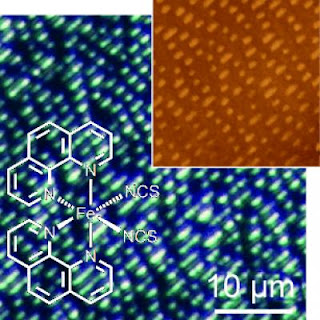
 Caption: This spin-transition compound can be nanopatterned by unconventional and soft lithography to give crystalline, well-oriented, micrometer-scale structures arranged in stripes on a silica surface, as revealed by optical and scanning force microscopy (inset). Credit: (C) Wiley-VCH 2008 Usage Restrictions: Permission to use with appropriate credit and link to dx.doi.org/10.1002/anie | Switchable nanostripes: Spin-transition compound can be deposited in ordered crystalline microstructures. In this information age, increased storage capacity is a central challenge for science and technology. A team of German and Italian researchers has pursued this by exploring the concept of "nanostructured storage domains". As the scientists, led by Massimiliano Cavallini at the National Research Council (CNR) in Bologna (Italy) and Mario Ruben at the Forschungszentrum Karlsruhe (Germany), report in the journal Angewandte Chemie, they have been able to produce reliable nanopatterns of a spin-transition compound on silicon oxide chips. |
Currently, computer hard drives store data by magnetizing the surface of a rotating disk. Each "storage cell" has an "address", so that stored data can be accessed directly. To increase storage capacity, the individual magnetic domains are made smaller and smaller; we are however getting close to the limit. Thermal excitation occasionally causes some of the magnetic particles to flip in the other direction. When the domains are very small, the entire cell can rapidly lose its magnetization.
To achieve higher information density, we could change to other switchable material properties, such as the transition between two spin states. For example, iron(II) compounds can exist in either a high- or a low-spin state. "Switching" (flipping) can be controlled by changes in temperature, pressure, or electromagnetic radiation.
In addition to two distinguishable states to represent 0 and 1, data storage also requires a unique "address" for each storage location that can be identified by the optical writing and reading units of the computer. This requires an interface that makes the nanoscopic spin-state transitions of the molecular switching units compatible with the microscale instrument environment. This is possible if the spin-transition compound can be put into a highly ordered micro- or nanostructure.
By using special unconventional micro- and nanolithographic techniques, the team was able to "print" a neutral iron(II) complex onto a silicon wafer in the form of very fine lines. In this process, the nanocrystals organize themselves into a preferred orientation along the line. Furthermore, the researchers were able to transfer the pattern of a recorded CD onto a film of this iron compound. This is the first proof that it is possible to produce readable logic patterns with a spin-transfer compound.
To make the stripe structures technologically useful, the switching process must be adapted to room-temperature conditions; work on this front is already at an advanced stage. ###
Author: Massimiliano Cavallini, CNR, Institute for Nanostructured Materials, Bologna (Italy), www.bo.ismn.cnr.it/staff Title: Micro- and Nanopatterning of Spin-Transition Compounds into Logical Structures Angewandte Chemie International Edition 2008, 47, No. 45, 8596?, doi: 10.1002/anie.200802085
Contact: Massimiliano Cavallini m.cavallini@bo.ismn.cnr.it 39-051-639-8519 Wiley-Blackwell


No comments:
Post a Comment