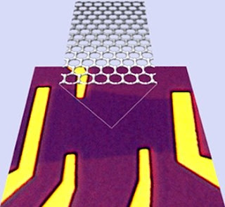
A team of researchers led by physics professor Michael S. Fuhrer of the university's Center for Nanophysics and Advanced Materials, and the Maryland NanoCenter said the findings are the first measurement of the effect of thermal vibrations on the conduction of electrons in graphene, and show that thermal vibrations have an extraordinarily small effect on the electrons in graphene.
"Other extrinsic sources in today's fairly dirty graphene samples add some extra resistivity to graphene," explained Fuhrer, "so the overall resistivity isn't quite as low as silver's at room temperature - yet. However, graphene has far fewer electrons than silver, so in graphene the electrical current is carried by only a few electrons moving much faster than the electrons in silver."
In semiconductors, a different measure, mobility, is used to quantify how fast electrons move. The limit to mobility of electrons in graphene is set by thermal vibration of the atoms and is about 200,000 cm2/Vs at room temperature, compared to about 1,400 cm2/Vs in silicon, and 77,000 cm2/Vs in indium antimonide, the highest mobility conventional semiconductor known.
"Interestingly, in semiconducting carbon nanotubes, which may be thought of as graphene rolled into a cylinder, we've shown that the mobility at room temperature is over 100,000 cm2/Vs," said Fuhrer
Mobility determines the speed at which an electronic device (for instance, a field-effect transistor, which forms the basis of modern computer chips) can turn on and off. The very high mobility makes graphene promising for applications in which transistors much switch extremely fast, such as in processing extremely high frequency signals.
Mobility can also be expressed as the conductivity of a material per electronic charge carrier, and so high mobility is also advantageous for chemical or bio-chemical sensing applications in which a charge signal from, for instance, a molecule adsorbed on the device, is translated into an electrical signal by changing the conductivity of the device.
Graphene is therefore a very promising material for chemical and bio-chemical sensing applications. The low resistivity and extremely thin nature of graphene also promises applications in thin, mechanically tough, electrically conducting, transparent films. Such films are sorely needed in a variety of electronics applications from touch screens to photovoltaic cells.
Fuhrer and co-workers showed that although the room temperature limit of mobility in graphene is as high as 200,000 cm2/Vs, in present-day samples the actual mobility is lower, around 10,000 cm2/Vs, leaving significant room for improvement. Because graphene is only one atom thick, current samples must sit on a substrate, in this case silicon dioxide. Trapped electrical charges in the silicon dioxide (a sort of atomic-scale dirt) can affect the electrons in graphene and reduce the mobility.
Also, vibrations of the silicon dioxide atoms themselves can also have an effect on the graphene which is stronger than the effect of graphene's own atomic vibrations. This so-called 'remote interfacial phonon scattering' effect is only a small correction to the mobility in a silicon transistor, but because the phonons in graphene itself are so ineffective at scattering electrons, this effect becomes very important in graphene.
"We believe that this work points out the importance of these extrinsic effects, and creates a roadmap for finding better substrates for future graphene devices in order to reduce the effects of charged impurity scattering and remote interfacial phonon scattering." Fuhrer said. ###
“Intrinsic and Extrinsic Performance Limits of Graphene Devices on SiO2,” J. H. Chen, C. Jang, S. Xiao, M. Ishigami, M. S. Fuhrer (will appear in Nature Nanotechnology online at 1800 London time, 1400 US Eastern time, March 23)
For More Information:
- About the paper, and Michael S. Fuhrer’s research laboratory, please visit physics.umd.edu/condmat/mfuhrer/
- About the University of Maryland, please visit umd.edu
- About the Department of Physics, please visit physics.umd.edu
- About the Center for Nanophysics and Advanced Materials, please visit cnam.umd.edu/
- About the Maryland NanoCenter, please visit nanocenter.umd.edu/
Tags: Nano or Nanotechnology and Nanotech or University of Maryland and Graphene or indium antimonide


No comments:
Post a Comment