Sunday, September 30, 2007

DNA Based Assembly of Nano Particles

New DNA-Based Technique For Assembly of Nano- and Micro-sized Particles
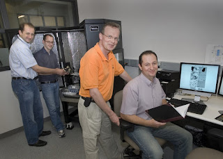
(From left) Dmytro Nykypanchuk and Mathew Maye load a sample into an atomic force microscope while Daniel van der Lelie and Oleg Gang review data at Brookhaven Labs Center for Functional Nanomaterials.UPTON, NY - Scientists at the U.S. Department of Energy's Brookhaven National Laboratory have developed a new method for controlling the self-assembly of nanometer and micrometer-sized particles.
The method, based on designed DNA shells that coat a particle's surface, can be used to manipulate the structure - and therefore the properties and potential uses - of numerous materials that may be of interest to industry. For example, such fine-tuning of materials at the molecular level promises applications in efficient energy conversion, cell-targeted systems for drug delivery, and bio-molecular sensing for environmental monitoring and medical applications.

The novel method, for which a patent application has been filed, was developed by Brookhaven researchers Mathew M. Maye, Dmytro Nykypanchuk, Daniel van der Lelie, and Oleg Gang and is described in the September 12 online edition of Small, a leading journal on nanoscience and nanotechnology.

"Our method is unique because we attached two types of DNA with different functions to particles' surfaces," said Gang, who leads the research team. "The first type - complementary single strands of DNA - forms a double helix. The second type is non-complementary, neutral DNA, which provides a repulsive force. In contrast to previous studies in which only complementary DNA strands are attached to the particles, the addition of the repulsive force allows for regulating the size of particle clusters and the speed of their self-assembly with more precision."

"When two non-complementary DNA strands are brought together in a fixed volume that is typically occupied by one DNA strand, they compete for space," said Maye. "Thus, the DNA acts as a molecular spring, and this results in the repulsive force among particles, which we can regulate. This force allows us to more easily manipulate particles into different formations."

The researchers performed the experiments on gold nanoparticles - measuring billionths of a meter - and polystyrene (a type of plastic) microparticles - measuring millionths of a meter. These particles served as models for the possibility of using the technique with other small particles. The scientists synthesized DNA to chemically react with the particles. They controlled the assembly process by keeping the total amount of DNA constant, while varying the relative fraction of complementary and non-complementary DNA. This technique allowed for regulating assembly over a very broad range, from forming clusters consisting of millions of particles to almost keeping individual particles separate in a non-aggregating form.

"It is like adjusting molecular springs," said Nykypanchuk. "If there are too many springs, particles will 'bounce' from each other, and if there are too few springs, particles will likely stick to each other."

The method was tested separately on the nano- and micro-sized particles, and was equally successful in providing greater control than using only complementary DNA in assembling both types of particles into large or small groupings.

To determine the structure of the assembled particles and to learn how to modify them for particular uses, the researchers used transmission electron microscopy to visualize the clusters, as well as x-ray scattering at the National Synchrotron Light Source to study particles in solution, the DNA's natural environment.

The Office of Basic Energy Sciences within the U.S. Department of Energy's Office of Science funded this research.

Contact: Diane Greenberg greenb@bnl.gov 631-344-2347 DOE/Brookhaven National Laboratory

Technorati Tags: or and and or and or Presidential Podcast 09/29/07 and Halloween Pumpkins and Taxol bristle ball: a wrench in the works for cancer

Saturday, September 29, 2007

Taxol bristle ball: a wrench in the works for cancer

Taxol bristle ball: a wrench in the works for cancer, Dozens of cancer-clogging drug molecules loaded onto tiny gold sphere

Caption: Using gold nanoparticles, Rice chemists have created tiny spheres that literally bristle with molecules of the anti-cancer drug Taxol. Credit: Eugene Zubarev/Rice University. Usage Restrictions: Must credit.HOUSTON, Sept. 12, 2007 – Rice University chemists have discovered a way to load dozens of molecules of the anti-cancer drug paclitaxel onto tiny gold spheres. The result is a tiny ball, many times smaller than a living cell that literally bristles with the drug.
Paclitaxel, which is sold under the brand name Taxol®, prevents cancer cells from dividing by jamming their inner works.

"Paclitaxel is one of the most effective anti-cancer drugs, and many researchers are exploring how to deliver much more of the drug directly to cancer cells," said lead researcher Eugene Zubarev, the Norman Hackerman-Welch Young Investigator and assistant professor of chemistry at Rice. "We looked for an approach that would clear the major hurdles people have encountered -- solubility, drug efficacy, bioavailability and uniform dispersion -- and our initial results look very promising."

The research is available online and will appear in the Sept. 19 issue of the Journal of the American Chemical Society (J. Am. Chem. Soc. 2007, vol. 129, pgs.11653-11661).

First isolated from the bark of the yew tree in 1967, paclitaxel is one of the most widely prescribed chemotherapy drugs in use today. The drug is used to treat breast, ovarian and other cancers.

Paclitaxel works by attaching itself to structural supports called microtubules, which form the framework inside living cells. In order to divide, cells must break down their internal framework, and paclitaxel stops this process by locking the support into place.

Since cancer cells divide more rapidly than healthy cells, paclitaxel is very effective at slowing the growth of tumors in some patients. However, one problem with using paclitaxel as a general inhibitor of cell division is that it works on all cells, including healthy cells that tend to divide rapidly. This is why patients undergoing chemotherapy sometimes suffer side effects like hair loss and suppressed immune function.

"Ideally, we'd like to deliver more of the drug directly to the cancer cells and reduce the side effects of chemotherapy," Zubarev said. "In addition, we'd like to improve the effectiveness of the drug, perhaps by increasing its ability to stay bound to microtubules within the cell."

Zubarev's new delivery system centers on a tiny ball of gold that's barely wider than a strand of DNA. Finding a chemical process to attach a uniform number of paclitaxel molecules to the ball -- without chemically altering the drugs -- was not easy. Only a specific region of the drug binds with microtubules. This region of the drugs fits neatly into the cell's support structure, like a chemical "key" fitting into a lock. Zubarev and graduate student Jacob Gibson knew they had to find a way to make sure the drug's key was located on the face of each bristle.

Zubarev and Gibson first designed a chemical "wrapper" to shroud the key, protecting it from the chemical reactions they needed to perform to create the ball. Using the wrapped version of the drug, they undertook a series of reactions to attach the drug to linker molecules that were, in turn, attached to the ball. In the final step of the reaction, they dissolved the wrapper, restoring the key.

"We are already working on follow-up studies to determine the potency of the paclitaxel-loaded nanoparticles," Zubarev said. "Since each ball is loaded with a uniform number of drug molecules, we expect it will be relatively easy to compare the effectiveness of the nanoparticles with the effectiveness of generally administered paclitaxel." ###

Research co-authors include Rice graduate student Bishnu Khanal. The research was funded by the National Science Foundation and the Welch Foundation.

Contact: Jade Boyd jadeboyd@rice.edu 713-348-6778 Rice University

Technorati Tags: or and and or and or President Bush Energy Security and Climate Change PODCAST VIDEO and Western Wall Wailing Wall and Biological interactions with nanomaterials

Friday, September 28, 2007

Biological interactions with nanomaterials

James E. Hutchison, Professor Organometallic and Materials ChemistryKeck Foundation funds study of biological interactions with nanomaterials, UO-ONAMI team to do pioneering study of designer nanoparticles for biomedical applications.

EUGENE, Ore.—(Sept. 10, 2007)—The University of Oregon has received a $1.6 million grant from the W.M. Keck Foundation to explore the biological effects of exposure to precisely engineered nanoparticles that are being designed for diagnostic and therapeutic uses.
The three-year grant from the Keck Foundation's medical research program will involve six researchers: Mark Lonergan, Jim Hutchison and Andy Berglund, all UO professors of chemistry; UO biology professors Karen Guillemin and Eric Johnson; and Robert Tanguay, a professor of environmental and molecular toxicology at Oregon State University.

All are members of the Safer Nanomaterials and Nanomanufacturing Initiative (SNNI), directed by Hutchison and part of the Oregon Nanoscience and Microtechnologies Institute (ONAMI).

"This award from the Keck Foundation puts us at the forefront of this quickly developing and promising field of nanotechnology," said UO President Dave Frohnmayer. "Nanotechnology has been described as being in its discovery phase. This newly funded project means the University of Oregon, Oregon State University and the state, through ONAMI – Oregon's first Signature Research Center – can help build a green roadmap for the field."

The interdisciplinary project is designed to help researchers understand potential biological interactions of engineered nanomaterials and develop design rules for the development of nanoparticles with enhanced biological properties. The researchers will produce specific structures of nanomaterials, investigate their interactions with biological systems and then design new materials and nanoparticle libraries that have specific biological responses.

The biological testing will involve laboratory experiments using zebrafish, an invertebrate animal model system that was first developed for research at the University of Oregon. With zebrafish, researchers can monitor tissue-specific interactions with nanoparticles, developmental and acute toxicity, and the impacts of exposure on gene regulation.

The researchers will address existing gaps in the field, from the basic construction of nanoparticles to how they interface with biological cells. As the foundation for the project, the group will build upon the library of gold nanoparticles created by Hutchison using his patented green-chemistry approach.

"Our goal is to define the important interactions at the bio-nano interface, as well as the ground rules for producing nanoparticles that have very fine-tuned objectives," Hutchison said. "The end results could lead to a variety of future therapeutics that specifically seek out and destroy cancer cells or promote desired cell growth for tissue regeneration."

The Keck Foundation funds will cover just under $1 million in graduate and faculty research, with the remainder going toward the purchase of equipment and space for housing it. The instruments will go into the Lorry I. Lokey Laboratories, the underground portion of the Integrated Science Complex, where some of the project's research will be conducted.

The W.M. Keck Foundation, based in Los Angeles, is one of the nation's largest philanthropic organizations. Established in 1954 by William Myron Keck, the founder of Superior Oil Co., the foundation provides funds primarily in the areas of medical research, science and engineering.

Contact: Jim Barlow jebarlow@uoregon.edu 541-346-3481 University of Oregon Source: Jim Hutchison, professor of chemistry, 541-346-4228

Technorati Tags: or and and or and or White House Press Briefing by Dana Perino 09/27/07 VIDEO PODCAST and St. Peter's Basilica and Drawing nanoscale features the fast and easy way

Thursday, September 27, 2007

Drawing nanoscale features the fast and easy way

Caption: The initials for the Georgia Institute of Technology written with the thermochemical nanolithography technique. Credit: Georgia Tech. Usage Restrictions: None.Scientists at the Georgia Institute of Technology have developed a new technique for nanolithography that is extremely fast and capable of being used in a range of environments including air (outside a vacuum) and liquids. Researchers have demonstrated the technique, known as thermochemical nanolithography, as a proof of concept.
The technique may allow industry to produce a variety of nanopatterned structures, including nanocircuits, at a speed and scale that could make their manufacture commercially viable. The research, which has potential applications for fields ranging from the electronics industry to nanofluidics to medicine, appeared earlier this year in the journal Nano Letters.

The technique is surprisingly simple. Using an atomic force microscope (AFM), researchers heat a silicon tip and run it over a thin polymer film. The heat from the tip induces a chemical reaction at the surface of the film. This reaction changes the film’s chemical reactivity and transforms it from a hydrophobic substance to a hydrophilic one that can stick to other molecules. The technique is extremely fast and can write at speeds faster than millimeters per second. That’s orders of magnitude faster than the widely used dip-pen nanolithography (DPN), which routinely clocks at a speed of 0.0001 millimeters per second.

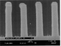
Using the new technique, researchers were able to pattern with dimensions down to 12 nanometers in width in a variety of environments. Other techniques typically require the addition of other chemicals to be transferred to the surface or the presence of strong electric fields. TCNL doesn’t have these requirements and can be used in humid environments outside a vacuum. By using an array of AFM tips developed by IBM, TCNL also has the potential to be massively scalable, allowing users to independently draw features with thousands of tips at a time rather than just one.

“Thermochemical nanolithography is a rapid and versatile technique that puts us much closer to achieving the speeds required for commercial applications,” said Elisa Riedo, assistant professor in Georgia Tech’s School of Physics. “Because we’re not transferring any materials from the AFM tip to the polymer surface (we are only heating it to change its chemical structure) this method can be intrinsically faster than other techniques.”

It’s the heated AFM tips that are one key to the new technique. Designed and fabricated by a group led by William King at the University of Illinois, the tips can reach temperatures hotter than 1,000 degrees Celsius. They can also be repeatedly heated and cooled 1 million times per second.

“The heated tip is the world’s smallest controllable heat source,” said King.

TCNL is also tunable. By varying the amount of heat, the speed and the distance of the tip to the polymer, researchers can introduce topographical changes or modulate the range of chemical changes produced in the material.

“By changing the chemistry of the polymer, we’ve shown that we can selectively attach new substances, like metal ions or dyes to the patterned regions of the film in order to greatly increase the technique’s functionality,” said Seth Marder, professor in Tech’s School of Chemistry and Biochemistry and director of the Center for Organic Photonics and Electronics. Marder’s group developed the thermally switchable polymers used in this study.

“We expect thermochemical nanolithography to be widely adopted because it’s conceptually simple and can be broadly applied,” said Marder. “The scope is limited only by one’s imagination to develop new chemistries and applications.”

Contact: David Terraso d.terraso@gatech.edu 404-385-2966 Georgia Institute of Technology

Technorati Tags: or and and or and or State Department Daily Press Briefing, 09/26/07 VIDEO and Dome of the Rock and Tiny Tubes and Rods Show Promise as Catalysts, Sunscreen

Wednesday, September 26, 2007

Tiny Tubes and Rods Show Promise as Catalysts, Sunscreen

New ways to make, modify titanium oxide nanostructures for industrial, medical uses

Wei-Qiang HanUPTON, NY - Scientists at the U.S. Department of Energy's Brookhaven National Laboratory have developed new ways to make or modify nanorods and nanotubes of titanium oxide, a material used in a variety of industrial and medical applications. The methods and new titanium oxide materials may lead to improved catalysts for hydrogen production, more efficient solar cells, and more protective sunscreens.
The research is published in two papers now available online, one in Advanced Materials (August 22, 2007), and the other in the Journal of Physical Chemistry (September 8, 2007).

In the first study, the scientists enhanced the ability of titanium oxide to absorb light.
Transmission electron micrographs of nanocavity-filled titanium oxide nanorods (bottom) and iron-doped titanate nanotubes (top). Both are being investigated as photocatalysts for reactions to produce hydrogen gas. The improved light-absorption of the nanocavity-filled nanorods also makes them ideal new materials for sunscreen
High Resolution Image
"Titanium dioxide's ability to absorb light is one the main reasons it is so useful in industrial and medical applications," said Wei-Qiang Han, a scientist at Brookhaven's Center for Functional Nanomaterials (CFN) and lead author on both papers. It is used as a photocatalyst for converting sunlight to electricity in solar cells and also has applications in the production of hydrogen, in gas sensors, in batteries, and in using sunlight to degrade some environmental contaminants. It is also a common ingredient in sunscreen.

Many scientists have explored ways to improve the light-absorbing capability of titanium oxide, for example, by "doping" the material with added metals. Han and his coworkers took a new approach. They enhanced the material's light-absorption capability by simply introducing nanocavities, completely enclosed pockets measuring billionths of a meter within the 100-nanometer-diameter solid titanium oxide rods.

The resulting nanocavity-filled titanium oxide nanorods were 25 percent more efficient at absorbing certain wavelengths of ultraviolet A (UVA) and ultraviolet B (UVB) solar radiation than titanium oxide without nanocavities.

"Our research demonstrates that titanium oxide nanorods with nanocavities can dramatically improve the absorption of UVA and UVB solar radiation, and thus are ideal new materials for sunscreen," Han said.

The cavity-filled nanorods could also improve the efficiency of photovoltaic solar cells and be used as catalysts for splitting water and also in the water-gas-shift reaction to produce pure hydrogen gas from carbon monoxide and water.

The method for making the cavity-filled rods is simple, says Han. "We simply heat titanate nanorods in air.
This process evaporates water, transforming titanate to titanium oxide, leaving very densely spaced, regular, polyhedral nanoholes inside the titanium oxide."

In the second paper, Han and his collaborators describe a new synthesis method to make iron-doped titanate nanotubes, hollow tubes measuring approximately 10 nanometers in diameter and up to one micrometer (one millionth of a meter) long. These experiments were also aimed at improving the material's photoreactivity. The scientists demonstrated that the resulting nanotubes exhibited noticeable reactivity in the water-gas-shift reaction.
"Although the activity of the iron-doped nanotubes was not as good as that of titanium oxide loaded with metals such as platinum and palladium, the activity we observed is still remarkable considering that iron is a much less expensive metal and its concentration in our samples was less than one percent," Han said.

The scientists also observed interesting magnetic properties in the iron-doped nanotubes, and will follow up with future studies aimed at understanding this phenomenon.

Materials developed in these studies were analyzed using several of Brookhaven Lab's
Wei-qiang Han (foreground), Lijun Wu, Zhen Xian, Yimei Zhu, and Wen Wen

Wei-qiang Han (foreground), Lijun Wu, Zhen Xian, Yimei Zhu, and Wen Wen
High Resolution Image
unique tools and methods for the characterization of nanostructures, including transmission electron microscopy and various techniques using x-ray and infrared beams at the Lab's National Synchrotron Light Source (NSLS).

This research, which has clear connections to improved energy technologies, was funded by the Office of Basic Energy Sciences within the U.S. Department of Energy's Office of Science.

Collaborators on the Advanced Materials paper include Lijun Wu, Robert F. Klie, and Yimei Zhu, all of Brookhaven's Center for Functional Nanomaterials (CFN). For the Journal of Physical Chemistry paper, collaborators include Brookhaven chemists Wen Wen and Jonathan Hanson; Ding Yi, Mathew Maye, and Oleg Gang of the CFN; Zhenxian Liu of the Carnegie Institution of Washington; and Laura Lewis, formerly at the CFN and now at Northeastern University.

Note to local editors: Wei-Qiang Han lives in East Setauket, New York.

Contact: Karen McNulty Walsh kmcnulty@bnl.gov 631-344-8350 DOE/Brookhaven National Laboratory

Technorati Tags: or and and or and or Mahmoud Ahmadinejad.United Nations VIDEO and William "Dummy" Hoy and Improved e-jet printing provides higher resolution and more versatility

Tuesday, September 25, 2007

Improved e-jet printing provides higher resolution and more versatility

Electric-field induced jets of functional organic electronic inks from nanoscale nozzles forms the basis of a technique, which researchers refer to as e-jet printing, to pattern electronics on flexible substrates.CHAMPAIGN, Ill. — By combining electrically induced fluid flow with nanoscale nozzles, researchers at the University of Illinois have established new benchmarks for precision control and resolution in jet-printing processes.

“We have invented methods for an electrohydrodynamic jet (e-jet) printing process that can produce patterns and functional devices that establish new resolution benchmarks for liquid printing,
significantly exceeding those of established ink-jet technologies,” said John Rogers, a Founder Professor of Materials Science and Engineering, and corresponding author of a paper accepted for publication in the journal Nature Materials, and posted on its Web site.

This type of e-jet printing could be used for large-area circuits, displays, photovoltaic modules and related devices, as well as other wide-ranging application possibilities in security, biotechnology and photonics, Rogers said.
The success of this effort relied critically on an interdisciplinary team of materials scientists, chemists, mechanical engineers, electrical engineers and physicists within the university’s Center for Nanoscale Chemical Electrical Mechanical Manufacturing Systems,extremely high-resolution form of e-jet printing can also be used for diverse systems,
a nanoscale science and engineering center funded by the National Science Foundation.

“As an industrial process, this work opens up the possibility for low-cost and
high-performance printed electronics and other systems that involve materials that cannot be manipulated with more common patterning methods derived from microelectronics fabrication,” said Placid Ferreira, the Grayce Wicall Gauthier Professor of Mechanical Science and Engineering, the director of the center and a key member of the team.
thin-film transistors that use aligned arrays of single-walled carbon nanotubes as the semiconductor and e-jet-printed source“The neat thing is that we find that this extremely high-resolution form of e-jet printing can also be used for diverse systems, such as printing microarrays of DNA spots for bioanalysis, or printing carbon nanotubes and other classes of nanomaterials that are difficult to pattern in other ways,”
said Rogers, who also is a researcher at the Beckman Institute and at the university’s Frederick Seitz Materials Research Laboratory. “These capabilities are taking our research in new and exciting directions.”

Unlike conventional ink-jet printers, which use heat or mechanical vibrations to launch liquid droplets through a nozzle, e-jet printing uses electric fields to pull the fluid out. Although the concept of electric-field induced flow is not new, the way the research team has exploited this phenomenon with nanoscale nozzles and precision control of electric fields to achieve unprecedented levels of resolution is an important advance.
The researchers’ e-jet printing head consists of a gold-coated microcapillary nozzle (with a diameter as small as 300 nanometers) mounted on a computer-controlled mechanical support. An organic, Teflon-like coating on the gold ensures the ink flows cleanly out the nozzle toward the target.suspensions of solid objects (such as nanoscale silicon rods) with resolutions again extending to the submicron range.
Tiny droplets of ink eject onto a moving substrate to produce printed patterns. Lines with widths as narrow as 700 nanometers, and dots as small as 250 nanometers, can be achieved in this fashion.

As a demonstration of electronic device fabrication by e-jet printing, thin-film transistors that use aligned arrays of single-walled carbon nanotubes as the semiconductor and e-jet-printed source and drain electrodes were printed on flexible plastic substrates. The transistors were fully operational, with properties comparable to similar devices fabricated with conventional photolithographic methods.
Current research seeks to improve the printing speed by incorporating large-scale nozzle arrays, and to explore the fundamental limits in resolution.The team also demonstrated that e-jet printing could be extended to a wide variety of functional organic and inorganic inks, including suspensions of solid objects (such as nanoscale silicon rods) with resolutions again extending to the submicron range.
Because the nozzles are routed directly to reservoirs of inks, e-jet printing has the capability to deliver large volumes of ink to a surface, and offers the ability to perform preprocessing on the inks before printing, Rogers said.

The existing e-jet printer can print text, drawings and images in a fully automated fashion. Current research seeks to improve the printing speed by incorporating large-scale nozzle arrays, and to explore the fundamental limits in resolution.

“The work represents an important milestone in the development of liquid-jet printing technology,” Rogers said, “which creates many exciting possibilities.”

Funding was provided by the National Science Foundation. Part of the work was carried out in the university’s Center for Microanalysis of Materials, which is partially supported by the U.S. Department of Energy.

Contact: James E. Kloeppel kloeppel@uiuc.edu 217-244-1073 University of Illinois at Urbana-Champaign

Editor’s note: To reach John Rogers, call 217-244-4979; e-mail: jrogers@uiuc.edu.

Technorati Tags: or and and or and or Racism's cognitive toll and United Nations Headquarters Building and Technology from outer space to playgrounds

Monday, September 24, 2007

Crucial difficulty in semiconductor device scaling

IBM and Imago find a crucial difficulty in semiconductor device scaling

Caption: Distribution of dopants revealed by atom probe. Credit: © Imago Scientific Instruments. Usage Restrictions: none.In 1959, Nobel Prize winner Richard Feynman presented a talk entitled “There's Plenty of Room at the Bottom. “ Feynman concluded that there was no physical reason why humans couldn't manipulate atoms.
However, if atomic manipulation is achieved the question of observing the new atom positions remains. How do you know what you have done"

As reported in the Sept. 7, 2007 issue of Science, IBM and Imago have taken a seminal step along the path to achieving Dr. Feynman’s vision by observing, for the first time, distributions of individual dopant atoms in semiconductor devices. Atom probe tomography was used to quantify the location and elemental identity of the atoms proximate to defects in silicon.

The dopants were implanted into the silicon uniformly and it was always hoped that the distribution of dopant atoms would be uniform. However, the IBM and Imago researchers found that clusters (more properly Cottrell atmospheres) of dopant atoms form around defects after ion implantation and annealing. Furthermore, these atmospheres persist in surrounding dislocation loops even after considerable thermal treatment creating dopant fluctuations that may ultimately limit the scalability of semiconductor devices.

“This is the first time that unambiguous quantitative 3D information regarding the precise location of individual dopant atoms relative to defects has been available” said study co-author and Imago CEO Tom Kelly. “The ability of the Imago LEAP 3000X Si laser assisted atom probe to make this measurement is the fruition of many years of instrumentation and applications development. We now have a powerful new way to probe the atomic positions of dopants in a semiconductor device. This is a critical tool for scientists seeking to answer Professor Feynman’s challenge to manipulate matter at the atomic level and hence enable nanotechnology.”

Previously, researchers have used secondary ion mass spectrometry (SIMS) and transmission electron microscopy (TEM) to correlate indirectly the presence of dopant atoms with the evolution of defects, and detailed models have been proposed to account for these experimental correlations. However, the atom probe study published in Science reports, for the first time, the location of individual dopant atoms.

Said Imago Senior Director of Applications and co-author David Larson, “The Sept. 7 Science article is the most recent in a series of significant scientific advances reported by Imago’s customers.” Added Dr. Larson, “In addition to producing breakthrough published scientific results, the Imago atom probe is also being applied to various industrial problems. These proprietary results are advancing scientific knowledge, enabling the development of new products, and improving time to market for our customers.” ###

Contact: Jason Schneir jschneir@imago.com 608-274-6880 x239 Imago Scientific Instruments

Technorati Tags: or and and or and or Racism's cognitive toll and United Nations Headquarters Building and Technology from outer space to playgrounds

Sunday, September 23, 2007

Technology from outer space to playgrounds

Caption: Professor Son is very pleased to receive this major award in only his second year at the University of Cincinnati. Credit: UC College of Engineering. Usage Restrictions: None.UC's NIH grant brings technology from outer space to playgrounds, From big people in tiny spaces to tiny people in big spaces: UC researchers adapt sensor technology developed for astronauts to monitor the health of children
Caretakers of children who are especially susceptible to air pollution (which can lead to increased risks of respiratory disease) will be able to identify locations in their everyday lives that contain high levels of particulate matter, thanks to research by an interdisciplinary team led by the University of Cincinnati and funded by the National Institutes of Health (NIH).
Sang Young Son, assistant professor in the University of Cincinnati College of Engineering, is principal investigator of the newly awarded $2 million, four-year project called ¡§Development and Field Test of a Positional Tagging Miniature Personal Sensor for PM1, sponsored by NIH's National Institute of Environmental Health Sciences (NIEHS).Caption: The sensor itself is tiny. The size of the monitor will be dictated by battery size. Credit: Sang Young Son. Usage Restrictions: None.
Son and his fellow researchers will use the grant to develop sensors for detecting and measuring particles in the air, which affect adults and children alike.

The interdisciplinary research team -- consisting of researchers at the UC colleges of Engineering and Medicine with collaborators at NASA Glenn Research Center in Cleveland, Ohio, and Washington University in St. Louis, Missouri -- plans to package condensate particulate counter sensors into miniature units utilizing microfluidics technologies that children can wear throughout the day. The team will integrate geographic information system technology developed at NASA into the sensors, allowing the exact location of specific exposures to be recorded.
Caption: Smaller sensors allow monitors to go with the patient instead of the patient going to the monitor. Credit: Sang Young Son. Usage Restrictions: None.Co-principal investigators consist of Da-Ren Chen, associate professor of mechanical engineering at Washington University; Paul S. Greenberg, NASA Glenn Research Center; Milind Jog, associate professor of mechanical engineering at the University of Cincinnati; Grace LeMasters,
professor and director of the molecular epidemiology in Children's Environmental Health Training at UC; James Lockey, professor of environmental health and internal medicine (pulmonary) at UC; and Patrick Ryan, research associate in environmental health at UC.

Before coming to UC in October 2005, Son worked at NASA Glenn Research Center, where he developed astronaut monitoring sensor technology.

"With NASA, we are looking at a confined environment in a space shuttle,"¨ Son says. "Now we expand the application to earth." The major difference between earth and space, as far as the sensor technology goes, is the gravitational force of earth.

"Our sensor uses liquid, which reacts to the gravitational force" says Son. ¡§Therefore, we need to add the capability to control the liquid."¨

Particles in the air on the order of one micron or less have the potential to initiate inflammatory and immune responses in human lungs. Because studies indicate that the effect might be cumulative, it's important to understand more about the exposure of humans, especially children, to particulate matter in their everyday lives. Currently, understanding the potential impact of particulate matter on human health is limited by the lack of knowledge of individuals' exposures to particle size and accumulation. Current sensors with the capability of detecting particles lack portability.

Until now, that is -- the sensors that the team is developing will be approximately the size of a deck of playing cards and fully wearable by the smallest earthling. With this portability comes the capability of monitoring individuals in remote locations, like playgrounds.

Lockey says, "The availability of this miniature sensor will greatly improve the capacity to identify the type and amount of environmental exposure that can result in a disease state."

"This will help correct the frequent misclassification to various environmental exposures that can occur in human studies," LeMasters adds.

The difference between the older technology and this new development is similar to the difference between a cell phone and a landline: one goes with the person; the other ties the person to a certain location.

"We can monitor every location, every individual," says Son.

Another major difference besides gravity is the size of the individual, as air particle densities vary with distance from the ground. "There's a distinct particle difference by height," Son notes.

During the first year of the grant, Washington University will be developing a device to cut test particles down to nano sizes with which the team will test the sensor. To be able to measure the sensor's performance accurately, the researchers will need standard size particles. The second step of the grant is developing a condensation mechanism, where the air particles are condensed and collected. This is Son's role. The third phase will be to develop an optical detection module to measure the particles that are collected in the sensor. Finally, they put the components of the system and test it. It is only after the second year that the exact shape of the sensor will have been derived. In the third year of the grant, the system will be calibrated and enhanced. Field testing will take place in the fourth year.

Once the wearable sensor technology has been successfully demonstrated, field tests will be with 8-year-old children participating in the University of Cincinnati Department of Environmental Health Cincinnati Childhood Allergy and Air Pollution Study (CCAAPS). Data generated by these field tests will help the researchers identify areas where the children are exposed to the highest concentrations of particulates.

Professor Son is very pleased to receive this major award in only his second year at the University of Cincinnati. Says Son, "The experience I gained working at NASA helped me to understand how the federal agencies work. The experience I gained working at Samsung Corporation helped me understand how to link research to product development. I drew upon that experience in proposing this work to NIH." ###

Contact: Wendy Hart Beckman wendy.beckman@uc.edu 513-556-1826 University of Cincinnati

Technorati Tags: or and and or and or Presidential Podcast 09/22/07 and Empire State Building and Superbugs, shapes and nanotechnology

Saturday, September 22, 2007

Superbugs, shapes and nanotechnology

Clostridium difficile is a bacterium commonly found in the intestinal tract but which, under the right circumstances such as after or during antibiotics therapy, can be the cause of enterocolitis. (Image courtesy of the Centers for Disease Control and Prevention.)A common hospital superbug called Clostridium has a protective coat of armour that can self assemble when put into a test tube on its own, which may have important commercial uses in nanotechnology,
according to scientists speaking at the Society for General Microbiology's 161st Meeting at the University of Edinburgh, UK, which ran from 3-6 September 2007.

Like many other micro-organisms, Clostridium difficile produces a lattice coat made of proteins to surround its cell wall and protect it like a suit of armour. The complete protein coat is then attached to the underlying cell wall with chemical bonds.

"We have discovered that these protein coats have a remarkable ability to self-assemble when they are taken off the bacteria and put into a test tube. Normally, on the bacteria, the proteins are not randomly arranged, they form regularly spaced geometrically arranged shapes, a bit like the rings in chain mail¡", says Dr Neil Fairweather of Imperial College London, UK. "We discovered that the proteins can do the same thing, and form the same distinct layers and shape, on their own in a test tube¡".

This finding opens up two areas of research for the science teams. It may lead to new ways of fighting hospital superbugs like Clostridium difficile by exposing weaknesses in the coats, or by identifying new target molecules. And in the new field of nanotechnology, where tiny particles are currently used in sunscreens and other products, finding ways to make molecules self assemble themselves into regular shapes could have important commercial applications.

"The field of nanotechnology is opening up to many new areas, and our research points to applications for this exciting technology in fighting superbugs like C. difficile¡" says Dr Fairweather. ###

Notes to News Editors:For further information contact Dr Neil Fairweather, Division of Cell and Molecular Biology, Imperial College London tel: 020 7594 5247, fax: 020 7594 3069, email: n.fairweather@imperial.ac.uk

Dr Fairweather is presenting the paper ¡¥Clostridium difficile and nanotechnology¡¦ at 1150 on Thursday 06 September 2007 in the Clinical Microbiology Group session of the 161st Meeting of the Society for General Microbiology at the University of Edinburgh, 03 Æ’{ 06 September 2007.

For press enquiries about the meeting please contact the SGM desk on +44 (0) 131 650 4581 or mobile telephone +44 (0) 7824 88 30 10

Full programme details of this meeting can be found on the Society's website at: sgm.ac.uk/meetings/MTGPAGES/Edinburgh07. Hard copies are available on request from the SGM.

The Society for General Microbiology is the largest microbiology society in Europe, and has over 5,500 members worldwide. The Society provides a common meeting ground for scientists working in research and in fields with applications in microbiology including medicine, veterinary medicine, pharmaceuticals, industry, agriculture, food, the environment and education.

The SGM represents the science and profession of microbiology to government, the media and the general public; supporting microbiology education at all levels; and encouraging careers in microbiology.

Contact: Lucy Goodchild l.goodchild@sgm.ac.uk 44-011-898-81843 Society for General Microbiology

Technorati Tags: or and and or and or National Rifle Association annual conference VIDEO and Brooklyn Bridge and Nanopantography Can Create Billions of Nanotech Devices

Friday, September 21, 2007

Nanopantography Can Create Billions of Nanotech Devices

NEW TECHNIQUE PRODUCING SMALL THINGS IN LARGE QUANTITIES, UH-Developed Nanopantography Can Create Billions of Nanotech Devices in Hours

HOUSTON, September 4, 2007 – Although relatively new to the market, liquid crystal display (LCD) televisions soon may be obsolete, thanks to a new technique created by University of Houston professors.

Schematic of an energetic (100s of eV) neutral beam source (left) and SEM picture of quarter-micron wide features (right) etched with this source in polymer using an O-atom beam. Neutral beam sources can mitigate charging effects that can cause serious problems in advanced microelectronics fabrication. Images: University of Houston Cullen College of EngineeringSchematic of an energetic (100s of eV) neutral beam source (left) and SEM picture of quarter-micron wide features (right) etched with this source in polymer using an O-atom beam. Neutral beam sources can mitigate charging effects that can cause serious problems in advanced microelectronics fabrication. Images: University of Houston Cullen College of Engineering
Schematic of an energetic (100s of eV) neutral beam source (left) and SEM picture of quarter-micron wide features (right) etched with this source in polymer using an O-atom beam. Neutral beam sources can mitigate charging effects that can cause serious problems in advanced microelectronics fabrication. Images: University of Houston Cullen College of Engineering

Vincent Donnelly, Demetre Economou and Paul Ruchhoeft, all of the Cullen College of Engineering, have developed a technique that allows nanotech devices to be mass-produced, which could move the television industry away from the LCD display to the superior field emission display (FED). FEDs use a large array of carbon nanotubes – the most efficient emitters known – to create a higher resolution picture than an LCD.

The nanotech fabrication technique that can mass produce an ordered array of carbon nanotubes and make FEDs happen promises to remove some of the largest practical barriers to mass-producing nanotech devices, Economou said.

Dubbed nanopantography, the method uses standard photolithography to selectively remove parts of a thin film and etching to create arrays of ion-focusing micro-lenses – small round holes through a metal structure – on a substrate, such as a silicon wafer.

“These lenses act as focusing elements,” Donnelly said. “They focus the beamlets to fabricate a hole 100 times smaller than the lens size.”

A beam of ions is then directed at the substrate. When the wafer is tilted, the desired pattern is replicated simultaneously in billions of many closely spaced holes over an area, limited only by the size of the ion beam.

“The nanostructures that you can form out of that focusing can be written simultaneously over the whole wafer in predetermined positions,” Economou said. “Without our technique, nanotech devices can be made with electron-beam writing or with a scanning tunneling microscope. However, the throughput, or fabrication speed, is extremely slow and is not suitable for mass production or for producing nanostructures of any desired shape and material.”

With the right ions and gaseous elements, the nanotech fabrication method can be used to etch a variety of materials and virtually any shape with nanosize dimensions. A standard printing technique that can create lenses measuring 100 nanometers wide could be used to draw features just one nanometer wide if combined with nanopantography.

“We expect nanopantography to become a viable method for rapid, large-scale fabrication,” Donnelly said. Economou, Donnelly and Ruchhoeft have been working on the technology for four years. UH filed the patent application in December 2006. They hope the technology can become commercially available in five to 10 years and expect it to become a viable method for large-scale production.

About the University of Houston, The University of Houston, Texas’ premier metropolitan research and teaching institution, is home to more than 40 research centers and institutes and sponsors more than 300 partnerships with corporate, civic and governmental entities. UH, the most diverse research university in the country, stands at the forefront of education, research and service with more than 35,000 students.

About the Cullen College of Engineering, UH Cullen College of Engineering has produced five U.S. astronauts, ten members of the National Academy of Engineering, and degree programs that have ranked in the top ten nationally. With more than 2,600 students, the college offers accredited undergraduate and graduate degrees in biomedical, chemical, civil and environmental, electrical and computer, industrial, and mechanical engineering. It also offers specialized programs in aerospace, materials, petroleum engineering and telecommunications.

Contact: Ann Holdsworth 713/743-8153 (office) 832/387-9322 (cell)aholdsworth@uh.edu

Technorati Tags: or and and or and or Press Conference by the President 09.20.07 VIDEO PODCAST and Transamerica Pyramid and NASA Technology Forms New Nanotechnology Company

Thursday, September 20, 2007

NASA Technology Forms New Nanotechnology Company

NASA Technology Forms the Basis for a New Nanotechnology Company

GREENBELT, Md. - A NASA-developed innovative process is making waves in the nanotechnology field and spurring the development of new companies in the process. A new company based in Austin, Texas, Nanotailor, has licensed NASA Goddard Space Flight Center's unique single-walled carbon nanotube (SWCNT) fabrication process with plans to make high-quality, low-cost SWCNTs available commercially.

NASA Goddard researcher Dr. Jeannette Benavides sets up her innovative, low-cost process for manufacturing carbon nanotubes, which has been licensed by Nanotailor and two other start-ups. Credit: NASA GSFC Innovative Partnerships Program Office.NASA Goddard researcher Dr. Jeannette Benavides sets up her innovative, low-cost process for manufacturing carbon nanotubes, which has been licensed by Nanotailor and two other start-ups. Credit: NASA GSFC Innovative Partnerships Program Office.
Potential markets for the technology are vast and include medical, construction, manufacturing, and imaging, to name just a few. The license provides Nanotailor a springboard from which to grow its business, while helping to make affordable nanotechnology available to a broad range of industries.

One of the basic nanotechnology structures, a carbon nanotube is a graphite sheet one atomic layer thick of carbon that is wrapped on itself to create an extraordinarily thin, strong tube. Although carbon nanotubes were discovered more than 15 years ago, their use has been limited due to the complex, dangerous, and expensive methods for their production.
NASA Goddard's innovative CNT manufacturing process uses helium arc welding to vaporize a carbon rod (anode), with the nanotubes forming in the soot deposited onto a water-cooled carbon cathode. Credit: NASA GSFC Innovative Partnerships Program Office.NASA Goddard's innovative CNT manufacturing process uses helium arc welding to vaporize a carbon rod (anode), with the nanotubes forming in the soot deposited onto a water-cooled carbon cathode. Credit: NASA GSFC Innovative Partnerships Program Office.
This unwieldy process has made SWCNTs cost-prohibitive up until now. "The nanotech industry is growing by more than 40 percent a year, but multi-walled carbon nanotubes have been the primary technology used. Single-walled technology just hasn’t taken off because of the cost," notes Nanotailor president Ramon Perales. "If we can get the cost down, we can be a step ahead and make higher quality nanotechnology more affordable."

NASA Goddard, located in Greenbelt, Md. is helping nanotechnology companies like Nanotailor do just that through a simpler, safer, and much less costly manufacturing process for SWCNTs. Developed by retired GSFC researcher Dr. Jeannette Benavides, the key to the innovation is the ability to produce bundles of SWCNTs without using a metal catalyst, dramatically reducing pre- and post-production costs while generating higher yields of better quality product. Other start-up companies that have licensed the process include Idaho Space Materials in Boise and E-City NanoTechnologies in the metro Baltimore area.
Thousands of times smaller than the average human hair, carbon nanotubes are extremely long and thin yet strong, making them a key nanotechnology structure. Credit: NASA Ames Research Center.Thousands of times smaller than the average human hair, carbon nanotubes are extremely long and thin yet strong, making them a key nanotechnology structure. Credit: NASA Ames Research Center.
With a license agreement in place, Nanotailor has built and tested a prototype based on NASA Goddard’s process, and is now working on commercialization efforts with a plan to go to market by the end of 2007. Device integrators and nanotechnology-based device companies will likely be among Nanotailor’s first customers, though the company hopes to cater to a wide variety of industries and research organizations. "All industries currently using multi-walled tubes will be able to benefit from this technology," notes Nanotailor chief technology officer Reginald Parker. "We’re lowering the cost per gram while greatly improving the integrity of the nanotubes. A better product at a lower price will help us bring higher quality nanotechnology to biomaterials, advanced materials, space exploration, highway and building construction… the list goes on and on."

This technology transfer success story was made possible by the efforts of NASA’s Innovative Partnerships Program (IPP), which has a two-part focus: (1) forming partnerships between NASA and industry, academia, or other government agencies to support the space program and (2) transferring NASA technology to new applications.

"NASA is committed to working with small businesses so they may be successful. It’s good for technology, for NASA, and for the U.S. economy," said Nona Minnifield Cheeks, Chief of the IPP Office at NASA Goddard.

Release No. 07-45, Contact: Rob Gutro Robert.J.Gutro@nasa.gov 301-286-4044 NASA/Goddard Space Flight Center

Related links:

Technorati Tags: or and and or and or White House Press Briefing by Dana Perino 09/19/07 VIDEO PODCAST and Sputnik: 50th Anniversary and Sustainable nanoelectronics, U.S.-Singapore

Wednesday, September 19, 2007

Sustainable nanoelectronics, U.S.-Singapore

Rice, Nanyang Tech collaborate on sustainable nanoelectronics, U.S.-Singapore team to leverage Moore’s Law for embedded computing BY JADE BOYD Rice News Staff

Computing researchers at Rice have joined electronics specialists at Singapore's Nanyang Technological University (NTU) to form a new $2.6-million Institute for Sustainable Nanoelectronics (ISNE). The joint research initiative, valued at 4 million Singapore dollars, aims to slash design and production costs for embedded microchips -- special-purpose computer chips that power everything from cell phones and digital cameras to jet airplanes and MRI machines.

Krishna V. Palem is the Kenneth and Audrey Kennedy Professor of Computing at the Department of Computer Science at the George Brown School of Engineering at Rice University.A major goal of the collaboration is to help sustain Moore's Law and exploit the exponential rate at which electronic components have been shrinking for more than four decades," said Rice researcher Krishna Palem, architect of the multinational initiative.
For instance, in a streaming video application on a cell phone, it's unnecessary to conduct precise calculations. The small screen, combined with the human brain's ability to process less-than-perfect pictures, results in a case where the picture looks just as good with a calculation that's only approximately correct.

The key is tying the costs for design, energy consumption and production to the value that the computed information has for the user," Palem said.

ISNE is funded by and based at NTU. It will draw upon an International Network of Excellence directed by Palem. The broad-based network will include computing experts from elite organizations like NTU, Rice and the Georgia Institute of Technology.

"Rice and NTU are well-positioned to lead the search for sustainable new technologies in nanoelectronics," said Rice President David Leebron. "NTU is a leader in electronics and a well-known contributor to Singapore's economic vitality. Rice is a leader in engineering and nanotechnology, with a well-deserved reputation for international collaboration and the development and application of new ideas."

The institute will partner with Rice's new Value of Information-based Sustainable Embedded Nanocomputing Center, or VISEN, which Palem recently established with seed funding from Rice.

"Palem, the Ken and Audrey Kennedy Professor in Computer Science and professor of electrical and computer engineering, joined Rice's faculty July 1 from Georgia Tech, where he founded and directed the Center for Research in Embedded Systems and Technology.
"Krishna was recruited to Rice by the legendary computer scientist Ken Kennedy," said Sallie Keller-McNulty, dean of Rice's George R. Brown School of Engineering. "Ken was passionate about optimization, about making all computers -- be they supercomputers or smart devices -- more efficient and easier to use.Krishna Palem (second from right) is working with Yeo Kiat Seng (right) and students at the Centre for Integrated Circuits and Systems at Nanyang Technological University in Singapore to develop the first production prototypes of a new type of power-stingy computer chip called PCMOS. NANYANG TECHNOLOGICAL UNIVERISTY
We're proud that Krishna is continuing the tradition of international excellence that Ken fostered at Rice."

ISNE hopes to evolve a design methodology that will be applicable not only to today's complementary metal–oxide semiconductors, or CMOS, but also to emerging computing platforms based on photonics and nanotechnology. The platform-independent approach is one of the institute's central themes, said Palem, who recently finished a yearlong appointment at the California Institute of Technology as a Gordon Moore Distinguished Scholar.

One example of the new "value-of-information" approach is probabilistic CMOS, or PCMOS, a new technology and an accompanying computing architecture invented within the past five years by Palem's research team. The key to PCMOS is a scheme that allows chips to trade off energy consumption at the cost of increased electronic "noise," which leads to slight processing errors.

"As information processing systems become more ubiquitous in consumer-driven applications, their designs must be tailored to reflect the needs of the end-users, and it is in this area that the new NTU/Rice Institute for Sustainable Nanoelectronics will make substantial contributions," said Ralph Cavin, chief scientist at the nonprofit Semiconductor Research Corporation in Durham, N.C. "The institute's goal of developing design technologies for extremelyscaled CMOS, so that the consumer's needs are met at reduced cost, is well-aligned with emerging directions in integrated circuit applications."

The beauty of PCMOS is that most of today's chips are over-engineered for day-to-day applications. In prior research, Palem ran cell-phone-style streaming video applications in a side-by-side comparison on PCMOS chips and traditional, power-hungry cell-phone chips. An award-winning demonstration of the technique at a 2006 conference in Seoul, South Korea, wowed audiences, who saw no appreciable difference in picture quality, even though the PCMOS chips used five times less power. Palem and colleagues at NTU are currently testing the first-generation production prototype PCMOS chips.

"NTU is pleased to be collaborating with Rice to spearhead research in sustainable nanoelectronics," said NTU President Su Guaning. "Leveraging the strengths of NTU and Rice, both top technological universities, will no doubt bring about exciting breakthroughs. We are also glad to have Professor Palem, renowned for his computing methodology, head the ISNE."

Contact: Jade Boyd jadeboyd@rice.edu 713-348-6778 Rice University

Technorati Tags: or and and or and or Michael B. Mukasey Biography and Lincoln Memorial and Nano tool to measure how environmental exposures affect health

Tuesday, September 18, 2007

Nano tool to measure how environmental exposures affect health

UCR engineers to develop new tool to measure how environmental exposures affect health, National Institutes of Health grant of $2.2 million to fund four-year research in nanotechnology.

Caption: UCR engineers involved in the research project. Clockwise from top left: Ashok Mulchandani (pricipal investigator of the grant), Marc Deshusses, Nosang Myung and David Cocker. Credit: Bourns College of Engineering, UC Riverside. Usage Restrictions: None.RIVERSIDE, Calif. – Engineers at UC Riverside’s Bourns College of Engineering have received a four-year $2.2 million grant from the National Institutes of Health (NIH), to be shared with researchers at Arizona State University, to develop a key tool for exploring the environmental roots of common diseases.
Employing nanotechnology to create the tool, the research project will be part of a new nationwide effort by NIH to better understand the underlying causes of increasingly common diseases such as diabetes, hypertension, asthma, arthritis, and Alzheimer’s disease, and the role that environmental exposures play in these diseases.

The project at UCR will involve the development of devices not available currently: inexpensive 4” by 4” badges, attachable to a person’s clothes, for monitoring diesel and gasoline exhaust exposure.

“The sensor we are developing would for the first time allow monitoring of over 40 components of diesel and gasoline exhaust simultaneously in real-time,” said Ashok Mulchandani, the principal investigator of the grant and a professor of chemical and environmental engineering. “Some of these exhaust toxics have been shown to cause respiratory illness and cancer.”

The light-weight badges will each house an array of electrochemical nanosensors for detecting and measuring exhaust. The measurements will be used eventually in studies focusing on what role diesel and/or gasoline exhaust play in causing disease. The badges also will be equipped with low-power microelectronics for power management, data collection and transfer, and signal processing.

“This NIH grant is a wonderful validation of the leadership role we play in sensor technology,” said Reza Abbaschian, dean of the Bourns College of Engineering. “The research this grant enables also supports our mission of providing excellent research and innovation to improve human health.”

An expert in biosensors, nanobiotechnology and biodetoxification, Mulchandani explained that the unique arrays of independent sensors in each badge will offer real-time analytical information on trace concentrations of air-borne toxics and pollutants, making it possible to selectively and accurately monitor personal exposure.

“The research project is a part of the college’s ongoing efforts in developing sensors for health care, environmental monitoring and homeland security,” he said.

Mulchandani will be joined in the research project by UCR’s Marc Deshusses, a professor of chemical and environmental engineering who will head the effort in modeling, experimental design and data analysis; Nosang Myung, an associate professor of chemical and environmental engineering who will provide expertise for nanoscale fabrication of the new sensor device; and David Cocker, an associate professor of environmental engineering who will lead the research on testing and validating the sensors, including their performance in real-time exposure conditions with diesel and gasoline exhaust.

They will collaborate with Arizona State University’s Joseph Wang, Bertan Bakkaloglu and Andreas Spanias, who will contribute expertise in chemical sensors, signal processing, and wireless communications.

UCR's Office of Technology Commercialization has pending patent applications that cover some aspects of the sensors that will be used in the experiment.

The grant is awarded by NIH's National Institute of Environmental Health Science, as part of the NIH “Genes, Environment and Health Initiative.” Multiple NIH agencies have invested a total of approximately $48 million for this inaugural year of the initiative. Expected to be funded for a total of four years, the initiative aims to analyze genetic variation in groups of patients with specific illnesses; and both produce and validate new methods for monitoring environmental exposures that interact with genetic variation to result in human diseases.

UCR will receive $1.5 million of the funding, with Arizona State University receiving the rest. For the inaugural year, the UCR project will receive nearly $567,000, with Arizona State University receiving approximately a third of this amount. The project is expected to begin this fall. ###

The Bourns College of Engineering (BCOE), established in 1989, is the one of the newest engineering schools in California and is ranked among the best public engineering colleges of its size in the nation. The faculty and student populations have both tripled in the past seven years, with new facilities and state-of-the-art laboratories, equipment and technology infrastructure keeping pace with the growth.

Interdisciplinary and collaborative efforts are a hallmark of the College in education, research and industrial partnerships, particularly in three affiliated research centers. BCOE offers an interdisciplinary major in Materials Science and Engineering, as well as B.S., M.S. and Ph.D. degrees through the five College departments: Bioengineering, Chemical & Environmental, Computer Science, Electrical and Mechanical.

The University of California, Riverside is a doctoral research university, a living laboratory for groundbreaking exploration of issues critical to Inland Southern California, the state and communities around the world. Reflecting California's diverse culture, UCR's enrollment of about 17,000 is projected to grow to 21,000 students by 2010.

The campus is planning a medical school and already has reached the heart of the Coachella Valley by way of the UCR Palm Desert Graduate Center. With an annual statewide economic impact of nearly $1 billion, UCR is actively shaping the region's future. To learn more, visit http://www.ucr.edu/ or call (951) UCR-NEWS.

Contact: Iqbal Pittalwala iqbal@ucr.edu 951-827-6050 University of California - Riverside

Technorati Tags: or and and or and or Michael Mukasey Nominee for Attorney General PODCAST VIDEO and The White House and Princeton engineers develop low-cost recipe for patterning microchips