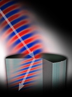
The new substance is in a relatively new class of materials called "metamaterials," which are made out of traditional substances, such as metals or semiconductors, arranged in very small alternating patterns that modify their collective properties. This approach enables metamaterials to manipulate light in ways that cannot be accomplished by normal materials.
Previous metamaterials were two-dimensional arrangements of metals, which limited their usefulness. The Princeton invention is the first three-dimensional metamaterial constructed entirely from semiconductors, the principal ingredient of microchips and optoelectronics.
"To be useful in a variety of devices, metamaterials need to be three-dimensional," said Princeton electrical engineering professor Claire Gmachl, one of the researchers on the study. "Furthermore, this is made from semiconductors, which are extremely functional materials. These are the things from which true applications are made."
The research team, led by Princeton engineering graduate student Anthony Hoffman, will publish its findings online Oct. 14 in the journal Nature Materials. Other Princeton researchers on the team include graduate students Leonid Alekseyev, Scott Howard and Kale Franz; former Council of Science and Technology fellow Dan Wasserman, now at the University of Massachusetts-Lowell; and former electrical engineering professor Evgenii Narimanov, now at Purdue University. The team also includes collaborators from Oregon State University and telecommunications firm Alcatel-Lucent.
Light waves and other forms of electromagnetic radiation bend whenever they pass from one medium to another. This phenomenon, called refraction, is readily observable when a straw placed into a glass of water appears to be bent or broken. Lenses in reading glasses or a camera work because of refraction.
In the case of the straw in a glass, normal water would make the underwater portion of the straw appear to bend toward the surface. If water were able to refract light negatively, as the newly invented semiconductor does, the segment of straw under the water would appear as if it were bending away from the surface.
Far more than a neat optical illusion, negative refraction holds promise for the development of superior lenses. The positive refractive indices of normal materials necessitate the use of curved lenses, which inherently distort some of the light that passes through them, in telescopes and microscopes. Flat lenses made from materials that exhibit negative refraction could compensate for this aberration and enable far more powerful microscopes that can "see" things as small as molecules of DNA.
In addition, the Princeton metamaterial is capable of negative refraction of light in the mid-infrared region, which is used in a wide range of sensing and communications applications. Its unique composition results in less lost light than previous metamaterials, which were made of extremely small arrangements of metal wires and rings. The semiconductors that constitute the new material are grown from crystals using common manufacturing techniques, making it less complex, more reliable and easier to produce.
"Currently, the typical infrared lens is a massive object -- the setups are bulky," Hoffman said. "This new material may enable more compact mid-infrared optics because we now have a new material with an entirely new set of optical parameters in our toolkit."
The research is part of a multi-institutional research center called Mid-Infrared Technologies for Health and the Environment (MIRTHE). Researchers at MIRTHE are developing compact sensors that detect trace amounts of gases in the atmosphere and human breath. These could one day be used in devices that monitor air quality and enhance homeland security, as well as in non-invasive and on-the-spot medical tests for diabetes and lung disease.
The research relies on a new type of laser that emits mid-infrared light. Gmachl, who directs the MIRTHE project, said the new material could be used to make the lasers better and smaller.
Next, the team plans to incorporate the new metamaterial into lasers. Additionally, the researchers will continue to modify the material in attempts to make features ever smaller in an effort to expand the range of light wavelengths they are able to manipulate.
The work was supported by the MIRTHE center and the Princeton Center for Complex Materials, both sponsored by the National Science Foundation.
Contact: Hilary Parker haparker@princeton.edu. 609-258-4597. Princeton University, Engineering School
Technorati Tags: Nano or Nanotechnology and Nanotech and metamaterials or Princeton University and optoelectronics or President Bush Heritage Foundation War on Terror VIDEO PODCAST and Ferrari 308GTS 240PS 1985 and Nanoengineers Mine Tiny Diamonds for Drug Delivery


No comments:
Post a Comment