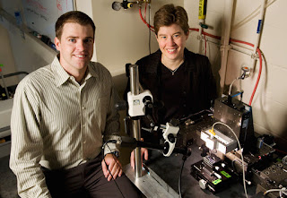
"Using this new family of inks, we have produced features as small as 225 nanometers," said co-author Jennifer Lewis, the Thurnauer Professor of Materials Science and Engineering and director of the university's Frederick Seitz Materials Research Laboratory (MRL). "Our goal is to get down to 100 nanometer feature sizes."
To create three-dimensional structures, the researchers use a robotic deposition process called direct-write assembly. The concentrated sol-gel ink is dispensed as a filament from a nozzle approximately 1 micron in diameter (about 100 times smaller than a human hair). The ink is dispensed while a computer-controlled micropositioner precisely directs the path. After the pattern for the first layer is complete, the nozzle is raised and another layer is deposited. This process is repeated until the desired shape is produced.
"We have opened direct ink writing to a new realm of functional materials," said graduate student Eric Duoss, the paper's lead author. "Since we print the desired functionality directly, the need for complicated templating and replicating schemes is eliminated."
Unlike previous inks, which require a liquid coagulation reservoir, the newly formulated inks are concentrated enough to rapidly solidify and maintain their shape in air, even as they span gaps in underlying layers.
"This gives us the ability to start, stop and reposition the flow of ink repeatedly, providing exquisite control over the deposition process," Duoss said. "For example, we can directly pattern defects in three-dimensional structures for use as photonic crystals."
After the structures have been assembled, they are converted to the desired functional oxide phase by heating at elevated temperature. Titanium dioxide, which possesses high refractive index and interesting electrical properties, is one material the researchers have successfully produced.
The researchers' ink design and patterning approach can be readily extended to other materials.
"There are a nearly endless variety of materials to choose from," Lewis said. "We envision having a toolbox of inks that can print at the micro- and nanoscale. These inks will be used for heterogeneous integration with other manufacturing techniques to create complex, functional devices composed of many different materials."
In addition to Lewis and Duoss, former post-doctoral researcher Mariusz Twardowski is a co-author of the paper.
Funding was provided by the U.S. Army Research Office. Part of the work was carried out in the Center for Microanalysis of Materials, which is partially supported by the U.S. Department of Energy and the University of Illinois.
Contact: James E. Kloeppel kloeppel@uiuc.edu, 217-244-1073. University of Illinois at Urbana-Champaign, Contact: Jennifer Lewis, 217/244-4973
Writer: James E. Kloeppel, physical sciences editor, Illinois News Bureau, 217/244-1073. Photo by L. Brian Stauffer.
Technorati Tags: Nano or Nanotechnology and Nanotech and Sol-gel inks or photonic crystals and University of Illinois at Urbana-Champaign or President Bush Urges Congress to Pass Appropriations Bills VIDEO PODCAST and Orson Welles War ot the Worlds H.G. Wells and New force-fluorescence device measures motion previously undetectable


No comments:
Post a Comment