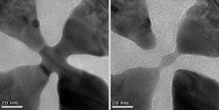
The technique employs transmission electron beam ablation lithography, or TEBAL, to “carve” nanostructures from thin sheets of gold, silver, aluminum and other metals. TEBAL provides a more dependable method for producing quality versions of these microscopic devices, which are studied for their novel mechanical properties and their potential use in next-generation sensors and electronics. The method also permits simultaneous, real-time atomic imaging of the devices as they are made.
Traditional techniques for building nanodevices employ electron beam lithography but also require the use of polymers and chemicals in which the metal is evaporated. Typical results are closer to 50 nanometers in size and rarely as small as 10.
Marija Drndiæ, professor of physics at Penn, and her team created nanodisks, nanorings, nanowires, nanoholes and multi-terminal nano-transistors. The results were published in the journal Nano Letters.
“Many different approaches have been undertaken to fabricate the small structures needed to probe the phenomena that take place at the nanoscale, but the most widely used and versatile techniques are limited to tens of nanometers,” Drndiæ said. “Reliably and consistently fabricating devices at the sub-10-nanometer scale from the top down is generally still challenging, but our technique offers a route to this regime.”
Furthermore, the TEBAL method creates a resistance-free connection between the nanostructure and an electrical lead that might provide power to the device. The more parts involved, the greater the chance of a drop in electrical conduction between parts. Plus, structures made from bottom-up techniques, i.e., assembled from smaller components, typically first need to be placed on a chip and then connected to larger circuitry. Working with a single piece of metal means there are no additional parts to reduce efficiency.
The team used the superior control of the electron beam to reproduce multiple, identical copies of each structure. The ability to rapidly produce these tiny devices will provide the samples needed for a better understanding of the mechanical and conductive properties of metal at the molecular scale. Future research may lead to computer-based creation of such devices with more intricacy and faster production cycles.
Superconducting circuits, magnets and molecule-sized transistors are among the real-world applications that may result from this research. Penn physicists also propose that a more rapid method of DNA sequencing can be developed from this process, by threading DNA strands through an electronic “nanoport” that could read the base pairs that constitute a species’ genetic code. ###
The study was conducted by Drndiæ and Michael Fischbein of Penn’s Department of Physics in the School of Arts and Sciences.
The research was supported by funding from the Office of Naval Research and the National Science Foundation.
Contact: Jordan Reese jreese@pobox.upenn.edu 215-573-6604 University of Pennsylvania
Technorati Tags: Nano or Nanotechnology and Nanotech and nanodevices or University of Pennsylvania and transmission electron beam ablation lithography or nanodisks, nanorings, nanowires, nanoholes and Nanotechnology: consumers must be convinced benefits outweigh risks or Famous People Elvis Presley and Whites Underestmate The Costs Of Being Black


No comments:
Post a Comment