Saturday, May 26, 2012

Record power conversion efficiency from a new graphene solar cell

GAINESVILLE, Fla. — Doping may be a no-no for athletes, but researchers in the University of Florida’s physics department say it was key in getting unprecedented power conversion efficiency from a new graphene solar cell created in their lab.

Graphene solar cells are one of industry’s great hopes for cheaper, durable solar power cells in the future. But previous attempts to use graphene, a single-atom-thick honeycomb lattice of carbon atoms, in solar cells have only managed power conversion efficiencies ranging up to 2.9 percent. The UF team was able to achieve a record breaking 8.6 percent efficiency with their device by chemically treating, or doping, the graphene with trifluoromethanesulfonyl-amide, or TFSA. Their results are published in the current online edition of Nano Letters.

“The dopant makes the graphene film more conductive and increases the electric field potential inside the cell,” said Xiaochang Miao, a graduate student in the physics department. That makes it more efficient at converting sunlight into electricity. And unlike other dopants that have been tried in the past, TFSA is stable — its effects are long lasting.


Xiaochang Miao
The solar cell that Miao and her co-workers created in the lab looks like a 5-mm-square window framed in gold. The window, a wafer of silicon coated with a monolayer of graphene, is where the magic happens.

Graphene and silicon, when they come together, form what is called a Schottky junction — a one-way street for electrons that when illuminated with light, acts as the power conversion zone for an entire class of solar cells. Schottky junctions are commonly formed by layering a metal on top of a semiconductor. But researchers at the UF Nanoscience Institute for Medical and Engineering Technologies discovered in 2011 that graphene, a semi-metal, made a suitable substitute for metal in creating the junction.

“Graphene, unlike conventional metals, is transparent and flexible, so it has great potential to be an important component in the kind of solar cells we hope to see incorporated into building exteriors and other materials in the future,” said Arthur Hebard, distinguished professor of physics at UF and co-author on the paper. “Showing that its power-converting capabilities can be enhanced by such a simple, inexpensive treatment bodes well for its future.”

The researchers said that if graphene solar cells reach 10 percent power conversion efficiency they could be a contender in the market place, if production costs are kept low enough.

The prototype solar cell created in the UF lab was built on a rigid base of silicon, which is not considered an economical material for mass production. But Hebard said that he sees real possibilities for combining the use of doped graphene with less expensive, more flexible substrates like the polymer sheets currently under development in research laboratories around the world. -30-

Credits Writer Donna Hesterman, donna.hesterman@ufl.edu, 352-846-2573 Source Arthur Hebard, afh@ufl.edu, 352-222-6212 Source Xiaochang Miao, xxmiaophy@gmail.com, 352-871-4116

Thursday, May 24, 2012

Topological Transitions in nanostructured Metamaterials

WEST LAFAYETTE, Ind. – Researchers are edging toward the creation of new optical technologies using "nanostructured metamaterials" capable of ultra-efficient transmission of light, with potential applications including advanced solar cells and quantum computing.

The metamaterial - layers of silver and titanium oxide and tiny components called quantum dots - dramatically changes the properties of light. The light becomes "hyperbolic," which increases the output of light from the quantum dots.

Such materials could find applications in solar cells, light emitting diodes and quantum information processing far more powerful than today's computers.

"Altering the topology of the surface by using metamaterials provides a fundamentally new route to manipulating light," said Evgenii Narimanov, a Purdue University associate professor of electrical and computer engineering.

nanostructured metamaterial

This graphic depicts a new "nanostructured metamaterial" - layers of silver and titanium oxide and tiny components called quantum dots - to dramatically change the properties of light. Researchers are working to perfect the metamaterials, which might be capable of ultra-efficient transmission of light, with potential applications including advanced solar cells and quantum computing. Findings and this image appeared in the journal Science in April. (Image courtesy of CUNY)
Such metamaterials could make it possible to use single photons – the tiny particles that make up light – for switching and routing in future computers. While using photons would dramatically speed up computers and telecommunications, conventional photonic devices cannot be miniaturized because the wavelength of light is too large to fit in tiny components needed for integrated circuits.

"For example, the wavelength used for telecommunications is 1.55 microns, which is about 1,000 times too large for today's microelectronics," Narimanov said.

Nanostructured metamaterials, however, could make it possible to reduce the size of photons and the wavelength of light, allowing the creation of new types of nanophotonic devices, he said.

The work was a collaboration of researchers from Queens and City Colleges of City University of New York (CUNY), Purdue University, and University of Alberta. The experimental study was led by the CUNY team, while the theoretical work was carried out at Purdue and Alberta.

The Science paper is authored by CUNY researchers Harish N.S. Krishnamoorthy, Vinod M. Menon and Ilona Kretzschmar; University of Alberta researcher Zubin Jacob; and Narimanov. Zubin is a former Purdue doctoral student who worked with Narimanov.

The approach could help researchers develop "quantum information systems" far more powerful than today's computers. Such quantum computers would take advantage of a phenomenon described by quantum theory called "entanglement." Instead of only the states of one and zero, there are many possible "entangled quantum states" in between.

The research has been funded by the National Science Foundation and the U.S. Army Research Office.

Purdue University Writer: Emil Venere, 765-494-4709, venere@purdue.edu Source: Evgenii Narimanov, 765-494-1622, enarimanov@gmail.com

Monday, May 21, 2012

Cloak of invisiblity a device that can see without being seen, an invisible machine that detects light and controls it's flow at the nanoscale

“plasmonic cloaking” a device that can see without being seen, an invisible machine that detects light and controls the flow of light at the nanoscale

A team of engineers at Stanford and the University of Pennsylvania has for the first time used “plasmonic cloaking” to create a device that can see without being seen – an invisible machine that detects light. It is the first example of what the researchers describe as a new class of devices that controls the flow of light at the nanoscale to produce both optical and electronic functions.

It may not be intuitive, but a coating of reflective metal can actually make something less visible, engineers at Stanford and UPenn have shown. They have created an invisible, light-detecting device that can “see without being seen.”

At the heart of the device are silicon nanowires covered by a thin cap of gold. By adjusting the ratio of metal to silicon – a technique the engineers refer to as tuning the geometries – they capitalize on favorable nanoscale physics in which the reflected light from the two materials cancel each other to make the device invisible.

Pengyu Fan is the lead author of a paper demonstrating the new device published online May 20th in the journal Nature Photonics. He is a doctoral candidate in materials science and engineering at Stanford University working in Professor Mark Brongersma’s group. Brongersma is senior author of the study.

Cloak of invisiblity


silicon nanowire

An image showing light scattering from a silicon nanowire running diagonally from bottom left to top right. The brighter areas are bare silicon while the dimmer sections are coated with gold demonstrating how plasmonic cloaking reduces light scattering in the gold-coated sections. Photo: Stanford Nanocharacterization Lab.
Light detection is well known and relatively simple. Silicon generates electrical current when illuminated and is common in solar panels and light sensors today. The Stanford device, however, is a departure in that for the first time it uses a relatively new concept known as plasmonic cloaking to render the device invisible.

The field of plasmonics studies how light interacts with metal nanostructures and induces tiny oscillating electrical currents along the surfaces of the metal and the semiconductor. These currents, in turn, produce scattered light waves.

By carefully designing their device – by tuning the geometries – the engineers have created a plasmonic cloak in which the scattered light from the metal and semiconductor cancel each other perfectly through a phenomenon known as destructive interference.

The rippling light waves in the metal and semiconductor create a separation of positive and negative charges in the materials – a dipole moment, in technical terms. The key is to create a dipole in the gold that is equal in strength but opposite in sign to the dipole in the silicon. When equally strong positive and negative dipoles meet, they cancel each other and the system becomes invisible.

“We found that a carefully engineered gold shell dramatically alters the optical response of the silicon nanowire,” said Fan. “Light absorption in the wire drops slightly – by a factor of just four – but the scattering of light drops by 100 times due to the cloaking effect, becoming invisible.”

“It seems counterintuitive,” said Brongersma, “but you can cover a semiconductor with metal – even one as reflective as gold – and still have the light get through to the silicon. As we show, the metal not only allows the light to reach the silicon where we can detect the current generated, but it makes the wire invisible, too.”

Broadly effective

The engineers have shown that plasmonic cloaking is effective across much of the visible spectrum of light and that the effect works regardless of the angle of incoming light or the shape and placement of the metal-covered nanowires in the device. They likewise demonstrate that other metals commonly used in computer chips, like aluminum and copper, work just as well as gold.

To produce invisibility, what matters above all is the tuning of metal and semiconductor.

“If the dipoles do not align properly, the cloaking effect is lessened, or even lost,” said Fan. “Having the right amount of materials at the nanoscale, therefore, is key to producing the greatest degree of cloaking.”

In the future, the engineers foresee application for such tunable, metal-semiconductor devices in many relevant areas, including solar cells, sensors, solid-state lighting, chip-scale lasers, and more.

In digital cameras and advanced imaging systems, for instance, plasmonically cloaked pixels might reduce the disruptive cross-talk between neighboring pixels that produces blur. It could therefore lead to sharper, more accurate photos and medical images.

“We can even imagine reengineering existing opto-electronic devices to incorporate valuable new functions and to achieve sensor densities not possible today,” concluded Brongersma. “There are many emerging opportunities for these photonic building blocks.”

Brongersma lab alumnus Professor Linyou Cao and doctoral candidate Farzaneh Afshinmanesh contributed to this research. This work is a collaboration with Professor Nader Engheta and post-doctoral researcher Uday Chettiar from University of Pennsylvania.

Andrew Myers is associate director of communications for the Stanford University School of Engineering.

Last modified Sun, 20 May, 2012 at 20:09 Media Contacts Andrew Myers Associate Director of Communications 650.736.2245 admyers@stanford.edu Jamie Beckett Director of Communications and Alumni Relations 650.736.2241 jbeckett@stanford.edu Stanford University. School of Engineering, 475 Via Ortega, Stanford, California 94305-4121. 650.725.1575

Thursday, May 17, 2012

Producing graphene quantum dots of controlled shape and size at large densities

Kansas State University researchers have come closer to solving an old challenge of producing graphene quantum dots of controlled shape and size at large densities, which could revolutionize electronics and optoelectronics.

Vikas Berry, William H. Honstead professor of chemical engineering, has developed a novel process that uses a diamond knife to cleave graphite into graphite nanoblocks, which are precursors for graphene quantum dots. These nanoblocks are then exfoliated to produce ultrasmall sheets of carbon atoms of controlled shape and size.

By controlling the size and shape, the researchers can control graphene’s properties over a wide range for varied applications, such as solar cells, electronics, optical dyes, biomarkers, composites and particulate systems. Their work has been published in Nature Communications and supports the university's vision to become a top 50 public research university by 2025. The article is available online.

"The process produces large quantities of graphene quantum dots of controlled shape and size and we have conducted studies on their structural and electrical properties," Berry said.


Graphene is a single atom thick sheet of sp2 hybridized carbon atoms arranged in a honeycomb lattice. With its dense cloud of charge carriers confined in atomic thickness and its large chemically modifiable surface area, graphene is a promising material for electronic sensing systems, electro-switches, biotechnology, and defense applications.
While other researchers have been able to make quantum dots, Berry's research team can make quantum dots with a controlled structure in large quantities, which may allow these optically active quantum dots to be used in solar cell and other optoelectronic applications.

"There will be a wide range of applications of these quantum dots," Berry said. "We expect that the field of graphene quantum dots will evolve as a result of this work since this new material has a great potential in several nanotechnologies."

It has been know that because of the edge states and quantum confinement, the shape and size of graphene quantum dots dictate their electrical, optical, magnetic and chemical properties. This work also shows proof of the opening of a band-gap in graphene nanoribbon films with a reduction in width. Further, Berry’s team shows through high-resolution transmission electron micrographs and simulations that the edges of the produces structures are straight and relatively smooth.

Other collaborators on this work include Zhiping Xu from Tsinghua University in China and David Moore from the University of Kansas. Xu conducted the molecular dynamics simulations. The co-authors from Kansas State University include Nihar Mohanty, 2011 doctoral graduate; T. S. Sreeprasad, postdoctoral fellow; Alfredo A. Rodriguez, 2012 graduate; and Ashvin Nagaraja, 2009 graduate.

The project was funded by the National Science Foundation and the office of naval research.

Berry earned his bachelor's degree in chemical engineering from the Indian Institute of Technology in Delhi, India, in 1999. He received his master's degree in chemical and petroleum engineering from the University of Kansas in 2003, followed by his doctorate in chemical engineering from Virginia Polytechnic Institute and State University in 2006.

Contact: Vikas Berry vberry@k-state.edu 785-532-5519 Kansas State University


Tuesday, May 15, 2012

New Plasmonic Component for Near-Infrared Metamaterials

WEST LAFAYETTE, Ind. - Researchers have taken a step toward overcoming a key obstacle in commercializing "hyperbolic metamaterials," structures that could bring optical advances including ultrapowerful microscopes, computers and solar cells.

The researchers have shown how to create the metamaterials without the traditional silver or gold previously required, said Alexandra Boltasseva, a Purdue University assistant professor of electrical and computer engineering.

Using the metals is impractical for industry because of high cost and incompatibility with semiconductor manufacturing processes. The metals also do not transmit light efficiently, causing much of it to be lost. The Purdue researchers replaced the metals with an "aluminum-doped zinc oxide," or AZO.

"This means we can have a completely new material platform for creating optical metamaterials, which offers important advantages," Boltasseva said.


Alexandra Boltasseva

Alexandra Boltasseva
Doctoral student Gururaj V. Naik provided major contributions to the research, working with a team to develop a new metamaterial consisting of 16 layers alternating between AZO and zinc oxide. Light passing from the zinc oxide to the AZO layers encounters an "extreme anisotropy," causing its dispersion to become "hyperbolic," which dramatically changes the light's behavior.

"The doped oxide brings not only enhanced performance but also is compatible with semiconductors," Boltasseva said.

Research findings are detailed in a paper appearing Monday (May 14) in the Proceedings of the National Academy of Sciences.

The list of possible applications for metamaterials includes a "planar hyperlens" that could make optical microscopes 10 times more powerful and able to see objects as small as DNA; advanced sensors; more efficient solar collectors; quantum computing; and cloaking devices.

The AZO also makes it possible to "tune" the optical properties of metamaterials, an advance that could hasten their commercialization, Boltasseva said.

"It's possible to adjust the optical properties in two ways," she said. "You can vary the concentration of aluminum in the AZO during its formulation. You can also alter the optical properties in AZO by applying an electrical field to the fabricated metamaterial."

This switching ability might usher in a new class of metamaterials that could be turned hyperbolic and non-hyperbolic at the flip of a switch.

"This could actually lead to a whole new family of devices that can be tuned or switched," Boltasseva said. "AZO can go from dielectric to metallic. So at one specific wavelength, at one applied voltage, it can be metal and at another voltage it can be dielectric. This would lead to tremendous changes in functionality."

The researchers "doped" zinc oxide with aluminum, meaning the zinc oxide is impregnated with aluminum atoms to alter the material's optical properties. Doping the zinc oxide causes it to behave like a metal at certain wavelengths and like a dielectric at other wavelengths.

The material has been shown to work in the near-infrared range of the spectrum, which is essential for optical communications, and could allow researchers to harness "optical black holes" to create a new generation of light-harvesting devices for solar energy applications.

The PNAS paper was authored by Naik, Boltasseva, doctoral student Jingjing Liu, senior research scientist Alexander V. Kildishev, and Vladimir M. Shalaev, scientific director of nanophotonics at Purdue's Birck Nanotechnology Center, a distinguished professor of electrical and computer engineering and a scientific adviser for the Russian Quantum Center.

Current optical technologies are limited because, for the efficient control of light, components cannot be smaller than the size of the wavelengths of light. Metamaterials are able to guide and control light on all scales, including the scale of nanometers, or billionths of a meter.

Unlike natural materials, metamaterials are able to reduce the "index of refraction" to less than one or less than zero. Refraction occurs as electromagnetic waves, including light, bend when passing from one material into another. It causes the bent-stick-in-water effect, which occurs when a stick placed in a glass of water appears bent when viewed from the outside. Each material has its own refraction index, which describes how much light will bend in that particular material and defines how much the speed of light slows down while passing through a material

Natural materials typically have refractive indices greater than one. Metamaterials, however, can make the index of refraction vary from zero to one, which possibly will enable applications including the hyperlens.

The layered metamaterial is a so-called plasmonic structure because it conducts clouds of electrons called "plasmons."

"Alternative plasmonic materials such as AZO overcome the bottleneck created by conventional metals in the design of optical metamaterials and enable more efficient devices," Boltasseva said. "We anticipate that the development of these new plasmonic materials and nanostructured material composites will lead to tremendous progress in the technology of optical metamaterials, enabling the full-scale development of this technology and uncovering many new physical phenomena."

This work has been funded in part by the U.S. Office of Naval Research, National Science Foundation and Air Force Office of Scientific Research

Writer: Emil Venere, 765-494-4709, venere@purdue.edu Source: Alexandra Boltasseva, 765-494-0301, aeb@purdue.edu

Sunday, May 13, 2012

Hydrogen-Evolution Catalysts Based on Non-Nobel Metal Nickel–Molybdenum Nitride Nanosheets

Hydrogen-Evolution Catalysts Based on Non-Nobel Metal Nickel–Molybdenum Nitride Nanosheets

UPTON, NY – Hydrogen gas offers one of the most promising sustainable energy alternatives to limited fossil fuels. But traditional methods of producing pure hydrogen face significant challenges in unlocking its full potential, either by releasing harmful carbon dioxide into the atmosphere or requiring rare and expensive chemical elements such as platinum.

Now, scientists at the U.S. Department of Energy’s (DOE) Brookhaven National Laboratory have developed a new electrocatalyst that addresses one of these problems by generating hydrogen gas from water cleanly and with much more affordable materials. The novel form of catalytic nickel-molybdenum-nitride – described in a paper published online May 8, 2012 in the journal Angewandte Chemie International Edition – surprised scientists with its high-performing nanosheet structure, introducing a new model for effective hydrogen catalysis.

“We wanted to design an optimal catalyst with high activity and low costs that could generate hydrogen as a high-density, clean energy source,” said Brookhaven Lab chemist Kotaro Sasaki, who first conceived the idea for this research. “We discovered this exciting compound that actually outperformed our expectations.”

Goldilocks chemistry


nanosheet structure

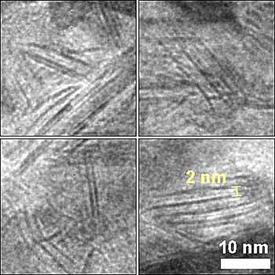
This magnified image from a transmission electron microscope reveals details of the unexpected nanosheet structure of the nickel-molybdenum-nitride catalyst, seen here as dark, straight lines
Water provides an ideal source of pure hydrogen – abundant and free of harmful greenhouse gas byproducts. The electrolysis of water, or splitting water (H2O) into oxygen (O2) and hydrogen (H2), requires external electricity and an efficient catalyst to break chemical bonds while shifting around protons and electrons. To justify the effort, the amount of energy put into the reaction must be as small as possible while still exceeding the minimum required by thermodynamics, a figure associated with what is called overpotential.

For a catalyst to facilitate an efficient reaction, it must combine high durability, high catalytic activity, and high surface area. The strength of an element’s bond to hydrogen determines its reaction level – too weak, and there’s no activity; too strong, and the initial activity poisons the catalyst.

“We needed to create high, stable activity by combining one non-noble element that binds hydrogen too weakly with another that binds too strongly,” said James Muckerman, the senior chemist who led the project. “The result becomes this well-balanced Goldilocks compound – just right.”

Unfortunately, the strongest traditional candidate for an electrocatlytic Goldilocks comes with a prohibitive price tag.
Problems with platinum

Platinum is the gold standard for electrocatalysis, combining low overpotential with high activity for the chemical reactions in water-splitting. But with rapidly rising costs – already hovering around $50,000 per kilogram – platinum and other noble metals discourage widespread investment.

“People love platinum, but the limited global supply not only drives up price, but casts doubts on its long-term viability,” Muckerman said. “There may not be enough of it to support a global hydrogen economy.”

In contrast, the principal metals in the new compound developed by the Brookhaven team are both abundant and cheap: $20 per kilogram for nickel and $32 per kilogram for molybdenum. Combined, that’s 1000 times less expensive than platinum. But with energy sources, performance is often a more important consideration than price.

Turning nickel into platinum

In this new catalyst, nickel takes the reactive place of platinum, but it lacks a comparable electron density. The scientists needed to identify complementary elements to make nickel a viable substitute, and they introduced metallic molybdenum to enhance its reactivity. While effective, it still couldn’t match the performance levels of platinum.

“We needed to introduce another element to alter the electronic states of the nickel-molybdenum, and we knew that nitrogen had been used for bulk materials, or objects larger than one micrometer,” said research associate Wei-Fu Chen, the paper’s lead author. “But this was difficult for nanoscale materials, with dimensions measuring billionths of a meter.”

The scientists expected the applied nitrogen to modify the structure of the nickel-molybdenum, producing discrete, sphere-like nanoparticles. But they discovered something else.

Subjecting the compound to a high-temperature ammonia environment infused the nickel-molybdenum with nitrogen, but it also transformed the particles into unexpected two-dimensional nanosheets. The nanosheet structures offer highly accessible reactive sites – consider the surface area difference between bed sheets laid out flat and those crumpled up into balls – and therefore more reaction potential.

Using a high-resolution transmission microscope in Brookhaven Lab’s Condensed Matter Physics and Materials Science Department, as well as x-ray probes at the National Synchrotron Light Source, the scientists determined the material’s 2D structure and probed its local electronic configurations.

“Despite the fact that metal nitrides have been extensively used, this is the first example of one forming a nanosheet,” Chen said. “Nitrogen made a huge difference – it expanded the lattice of nickel-molybdenum, increased its electron density, made an electronic structure approaching that of noble metals, and prevented corrosion.”

Hydrogen future

The new catalyst performs nearly as well as platinum, achieving electrocatalytic activity and stability unmatched by any other non-noble metal compounds. “The production process is both simple and scalable,” Muckerman said, “making nickel-molybdenum-nitride appropriate for wide industrial applications.”

While this catalyst does not represent a complete solution to the challenge of creating affordable hydrogen gas, it does offer a major reduction in the cost of essential equipment. The team emphasized that the breakthrough emerged through fundamental exploration, which allowed for the surprising discovery of the nanosheet structure.

“Brookhaven Lab has a very active fuel cell and electrocatalysis group,” Muckerman said. “We needed to figure out fundamental approaches that could potentially be game-changing, and that’s the spirit in which we’re doing this work. It’s about coming up with a new paradigm that will guide future research.”

Additional collaborators on this research were: Anatoly Frenkel of Yeshiva University, Nebojsa Marinkovic of the University of Delaware, and Chao Ma, Yimei Zhu and Radoslav Adzic of Brookhaven Lab.

The research was funded by Brookhaven's Laboratory Directed Research and Development (LDRD) Program. The National Sychrotron Light Source and other Brookhaven user facilities are supported by the DOE Office of Science. +sookie tex

DOE’s Office of Science is the single largest supporter of basic research in the physical sciences in the United States, and is working to address some of the most pressing challenges of our time. For more information, please visit science.energy.gov.

Contact: Justin Eure jeure@bnl.gov 631-344-2347 DOE/Brookhaven National Laboratory

Friday, May 11, 2012

New nanometer-scale atomic structure in solid metallic materials known as metallic glasses

Drawing on powerful computational tools and a state-of-the-art scanning transmission electron microscope, a team of University of Wisconsin-Madison and Iowa State University materials science and engineering researchers has discovered a new nanometer-scale atomic structure in solid metallic materials known as metallic glasses.

Published May 11 in the journal Physical Review Letters, the findings fill a gap in researchers' understanding of this atomic structure. This understanding ultimately could help manufacturers fine-tune such properties of metallic glasses as ductility, the ability to change shape under force without breaking, and formability, the ability to form a glass without crystalizing.

Glasses include all solid materials that have a non-crystalline atomic structure: They lack a regular geometric arrangement of atoms over long distances. "The fundamental nature of a glass structure is that the organization of the atoms is disordered-jumbled up like differently sized marbles in a jar, rather than eggs in an egg carton," says Paul Voyles, a UW-Madison associate professor of materials science and engineering and principal investigator on the research.


Paul Voyles

Paul Voyles
Researchers widely believe that atoms in metallic glasses are arranged only as pentagons in an order known as five-fold rotational symmetry. However, in studies of a zirconium-copper-aluminum metallic glass, Voyles' team found there are clusters of squares and hexagons-in addition to clusters of pentagons, some of which form chains-all located within the space of just a few nanometers. "One or two nanometers is a group of about 50 atoms-and it's how those 50 atoms are arranged with respect to one another that's the new and interesting part," he says.

Measuring the atomic structure of glass at this scale has been extremely difficult. Researchers know that, at a few tenths of a nanometer, atoms in metallic glasses have the same distances between them as they do in crystals. They also know that at long distances-hundreds of nanometers-there's no order left. "But what happens in between, at this 'magic' length of one to three nanometers, is very hard to measure experimentally and is essentially unexplored in experiments and simulations," says Voyles.

An expert in electron microscopy, Voyles used a powerful, state-of-the-art scanning transmission electron microscope at UW-Madison as his window into this nanometer-scale atomic structure. The microscope can generate an electron probe beam two nanometers in diameter-the ideal size for examining atoms on a length scale of one to three nanometers. "And that, fundamentally, is what makes the experiments work and gives us access to this information that's otherwise very difficult to obtain," he says. "We can match our experimental probe in size right to the size of what we want to measure."

Voyles and his team coupled the experimental data from the microscope with state-of-the-art computational methods to conduct simulations that accurately reflect the experiments. "It's the combination of those two things that gives us this new insight," he says. "We can look at the results and abstract general principles about rotational symmetry and nanoscale clustering."

There were several clues in the properties of some metallic glasses that these competing geometric structures might exist. Those arise from the interrelationships of structure, processing and properties, says Voyles. "If we understand how the structure controls, for example, glass-forming ability or the ability to change shape on bending or pulling, and we understand how different elements participate in these different kinds of structures, that gives us a handle on controlling properties by adjusting the composition or adjusting the rate at which the material was cooled or heated to change the structure in some useful way," he says.

One of the unique characteristics of glasses is their ability to transition continuously from a solid to a liquid state. While other materials, when heated,
are partly melted and partly solid, glasses as a whole become increasingly malleable.

While manufacturers now apply metallic glasses primarily in electrical transformer cores, their special forming capabilities may enable manufacturers to make very small, intricate parts. "Unlike conventional metallic alloys, metallic glasses can be molded like plastic-so they can be pushed or sucked or blown into very complicated shapes without any loss of material or machining," says Voyles.

Those manufacturing methods hold true even at the micro or nanoscale, so it's possible to make, for example, forests of nanowires or the world's smallest geared motor. "Five or 10 years from now, there may be more commercial applications driven by those kinds of things than there are now," he says.

For Voyles and his team, the next step will be to calculate the properties of the most realistic structural models of metallic glass they have developed to learn how those properties relate to the structure.

Other authors on the Physical Review Letters paper include lead author Jinwoo Hwang, Z.H. Melgarejo and Don Stone of UW-Madison, and Y.E. Kalay, I. Kalay and M.J. Kramer of Iowa State University.

The National Science Foundation funded Voyles' research and an NSF grant enabled him and other UW-Madison collaborators to purchase the scanning transmission electron microscope. Installed in 2010, the microscope can be operated remotely and provides UW-Madison researchers a level of instrumentation on par with the world-leading federal laboratories and research universities.

Contact: Paul Voyles voyles@engr.wisc.edu 608-265-6740 University of Wisconsin-Madison

Wednesday, May 09, 2012

Quantum dot technologies create highly efficient form of solid-state lighting that produces high quality white light

Quantum dot  technologies create highly efficient form of solid-state lighting that produces high quality white light.

With the age of the incandescent light bulb fading rapidly, the holy grail of the lighting industry is to develop a highly efficient form of solid-state lighting that produces high quality white light.

One of the few alternative technologies that produce pure white light is white-light quantum dots. These are ultra-small fluorescent beads of cadmium selenide that can convert the blue light produced by an LED into a warm white light with a spectrum similar to that of incandescent light. (By contrast, compact fluorescent tubes and most white-light LEDs emit a combination of monochromatic colors that simulate white light).

Seven years ago, when white-light quantum dots were discovered accidentally in a Vanderbilt chemistry lab, their efficiency was too low for commercial applications and several experts predicted that it would be impossible to raise it to practical levels. Today, however, Vanderbilt researchers have proven those predictions wrong by reporting that they have successfully boosted the fluorescent efficiency of these nanocrystals from an original level of three percent to as high as 45 percent.
Potential commercial applications

Scanning electron microscope image of a quantum dot that shows the individual atoms. (Rosenthal Lab)

Scanning electron microscope image of a quantum dot that shows the individual atoms. (Rosenthal Lab)

“Forty-five percent is as high as the efficiency of some commercial phosphors which suggests that white-light quantum dots can now be used in some special lighting applications,” said Sandra Rosenthal, the Jack and Pamela Egan Chair of Chemistry, who directed the research which is described online in the Journal of the American Chemical Society. “The fact that we have successfully boosted their efficiency by more than 10 times also means that it should be possible to improve their efficiency even further.”

The general measure for the overall efficiency of lighting devices is called luminous efficiency and it measures the amount of visible light (lumens) a device produces per watt. An incandescent light bulb produces about 15 lumens/watt, while a fluorescent tubes put out about 100 lumens/watt. White light LEDs currently on the market range from 28 to 93 lumens/watt.

“We calculate that if you combine our enhanced quantum dots with the most efficient ultraviolet LED, the hybrid device would have a luminous efficiency of about 40 lumens/watt,” reported James McBride, research assistant professor of chemistry who has been involved in the research from its inception. “There is lots of room to improve the efficiency of UV LEDS and the improvements would translate directly into a higher efficiencies in the hybrid.”

An accidental discovery

Quantum dots were discovered in 1980. They are beads of semiconductor material – the stuff from which transistors are made – that are so small that they have unique electronic properties, intermediate between those of bulk semiconductors and individual molecules. One of their useful properties is fluorescence that produces distinctive colors determined by the size of the particles. As the nanocrystal’s size shrinks the light it emits shifts from red to blue. The Vanderbilt discovery was that ultra-small quantum dots, containing only 60 to 70 atoms, emit white instead of monochromatic light.

“These quantum dots are so small that almost all of the atoms are on the surface, so the white-light emission is intrinsically a surface phenomena,” said Rosenthal.

One of the first methods various groups used in the attempt to brighten the nanocrystals was “shelling” – growing a shell around them made of a different material, like zinc sulfide. Unfortunately, the shells extinguished the white light effect and the shelled quantum dots produced only colored light.
Chemists followed their noses

Following a lead from some research done at the University of North Carolina, the researchers decided to see if treating the quantum dots with metal salts would have a brightening effect. They noticed that some of the salts seemed to produce a small – 10 to 20 percent – but noticeable improvement.

“They were acetate salts and they smelled a bit like acetic acid,” said McBride. “We knew that acetic acid binds to the quantum dots so we decided to give it a try.”

The decision to follow their nose proved to be fortunate. The acetic acid treatment bumped up the quantum dots fluorescent efficiency from eight percent to 20 percent!

Acetic acid is a member of the carbocyclic acid family. So the researchers tried the other members in the family. They found that the simplest and most acidic member – formic acid, the chemical that ants use to mark their paths – worked the best, pushing the efficiency as high as 45 percent.

The brightness boost had an unexpected side effect. It shifted the peak of the color spectrum of the quantum dots slightly into the blue. This is ironic because the major complaint of white-light LEDs is that the light they produce has an unpleasant blue tint. However, the researchers maintain that they know how to correct the color-balance of the boosted light.

The researchers’ next step is to test different methods for encapsulating the enhanced quantum dots.

Other contributors to the study include graduate students Teresa E. Rosson, Sarah M. Claiborne and undergraduate research student Benjamin Stratton, who is now at Columbia University.

The work was supported by a grant from the National Science Foundation. +sookie tex

TEXT and IMAGE CREDIT: Vanderbilt University Nashville, Tennessee 37240 · (615) 322-7311 Contact: David Salisbury, (615) 322-NEWS david.salisbury@vanderbilt.edu by | Posted on Tuesday, May. 8, 2012 — 2:56 PM

Monday, May 07, 2012

Helmholtz-Zentrum Dresden-Rossendorf International Helmholtz Research School for Nanoelectronic Networks support Next Generation of Nanoelectronic Scientists

Helmholtz-Zentrum Dresden-Rossendorf International Helmholtz Research School for Nanoelectronic Networks support Next Generation of Nanoelectronic Scientists.

In order to successfully promote the next generation of superb scientists for the microelectronics venue Dresden, the Helmholtz-Zentrum Dresden-Rossendorf (HZDR) founded the International Helmholtz Research School for Nanoelectronic Networks NANONET together with the TU Dresden [Dresden University of Technology], the Leibniz Institute for Polymer Research Dresden, the Fraunhofer Institute for Nondestructive Testing (IZFP), and the NaMLab gGmbH corporation. It will be supported annually with 200,000 euros over the next six years by the Helmholtz Association’s Initiative and Networking Fund.

The International Helmholtz Research School NANONET is a structured doctoral program which promotes the education of the next generation of scientists in molecular electronics while at the same time striving to advance this field of research. It seeks to determine how atoms and molecules may be functionalized and designed so that they can switch information; thus, making them the smallest possible transistors. That’s at least what the scientists are hoping to accomplish who are working together with Dr. Artur Erbe from the HZDR. Dr. Erbe is also the spokesperson of the new International Helmholtz Research School: “At the moment, individual molecules are the smallest components imaginable which can be integrated into a processor. It’s our vision to develop components which create a circuit all by themselves. That’s a really exciting research field which should drastically lower production costs in the chip industry by significantly reducing the consumption of energy,” notes Artur Erbe.

The Dresden-based Helmholtz-Kolleg NANONET Picture: Katrin Kerbusch

The Dresden-based Helmholtz-Kolleg NANONET Picture: Katrin Kerbusch
This research approach belongs to the “bottom up methods” in which many scientists see the future of microelectronics. Because with the current “top down” technologies, transistors may only be reduced up to a specific size which according to the American entrepreneur Gordon Moore will be reached soon. That’s why scientists are taking the opposite approach today by constructing complex structures out of individual molecules and atoms. “Within the scope of the research alliance DRESDEN-concept, we’re already conducting intense research in this field with our partners. And now we want to deliberately foster the next generation of scientific researchers,” notes Artur Erbe.

Every three years, up to 25 international doctoral candidates will be educated in the International Helmholtz Research School NANONET. Applicants are welcome from such diverse fields as physics, chemistry, electrical engineering, and materials science. They have to participate in a selection process and present a topic that’s of relevance to molecular electronics and about which they plan to write their dissertation. The successful candidates who are selected for the NANONET doctoral program will get, on the one hand, a thorough and highly interdisciplinary scientific education; including the possibility of conducting their doctoral studies with greater flexibility than usual. The doctoral program also conveys specific knowledge in research management which is becoming increasingly more relevant to the career of scientists today, for example, when seeking to successfully procure third-party funding. Every doctoral candidate will be supervised by a scientist at one of the five partner institutes. Academically, the NANONET doctoral program will be carried out at three TU Dresden faculties (mechanical science and engineering, electrical and computer engineering, mathematics and natural sciences) with a specific focus on an interdisciplinary education. The Research School with its 15 renowned scientists has, thus, a clear strategy to ensure the successful cooperation between the various fields.

In addition to NANONET, the Helmholtz Association is also supporting four other International Helmholtz Research Schools and two Helmholtz Graduate Schools this year in order to provide the best possible support to the next generation of researchers while they’re still doctoral candidates.

For more information, please contact: Dr. Artur Erbe Helmholtz-Zentrum Dresden-Rossendorf Spokesperson of the Helmholtz Research School Phone 0351 260-2366

Prof. Dr. Gianaurelio Cuniberti Chair of Materials Science and Nanotechnology Faculty of Mechanical Science and Engineering TU Dresden Phone 0351 463 31420

Press Contact: Dr. Christine Bohnet Helmholtz-Zentrum Dresden-Rossendorf Press Officer Phone 0351 260-2450 oder 0160 969 288 56 Kim-Astrid Magister TU Dresden Press Officer Phone 0351 463 32398

Wednesday, May 02, 2012

Liquid crystals to spontaneously create nanoscale morphologies we didn't know existed

MADISON – Liquid crystals, the state of matter that makes possible the flat screen technology now commonly used in televisions and computers, may have some new technological tricks in store.

Writing today (May 3, 2012) in the journal Nature, an international team of researchers led by University of Wisconsin-Madison Professor of Chemical and Biological Engineering Juan J. de Pablo reports the results of a computational study that shows liquid crystals, manipulated at the smallest scale, can unexpectedly induce the molecules they interact with to self-organize in ways that could lead to entirely new classes of materials with new properties.

"From an applied perspective, once we get to very small scales, it becomes incredibly difficult to pattern the structure of materials. But here we show it is possible to use liquid crystals to spontaneously create nanoscale morphologies we didn't know existed," says de Pablo of computer simulations that portray liquid crystals self-organizing at the molecular scale in ways that could lead to remarkable new materials with scores of technological applications.


nanospheres of liquid crystal materials

A computational model shows nanospheres of liquid crystal materials. The different patterns represent the self organization of surfactants, the molecules the liquid crystals interact with at their surface interface.Image: Juan de Pablo.
As their name implies, liquid crystals exhibit the order of a solid crystal but flow like a liquid. Used in combination with polarizers, optical filters and electric fields, liquid crystals underlie the pixels that make sharp pictures on thin computer or television displays. Liquid crystal displays alone are a multibillion dollar industry. The technology has also been used to make ultrasensitive thermometers and has even been deployed in lasers, among other applications.

The new study modeled the behavior of thousands of rod-shaped liquid crystal molecules packed into nano-sized liquid droplets. It showed that the confined molecules self organize as the droplets are cooled. "At elevated temperatures, the droplets are disordered and the liquid is isotropic," de Pablo explains. "As you cool them down, they become ordered and form a liquid crystal phase. The liquid crystallinity within the droplets, surprisingly, induces water and other molecules at the interface of the droplets, known as surfactants, to organize into ordered nanodomains. This is a behavior that was not known."

In the absence of a liquid crystal, the molecules at the interface of the droplet adopt a homogeneous distribution. In the presence of a liquid crystal, however, they form an ordered nanostructure. "You have two things going on at the same time: confinement of the liquid crystals and an interplay of their structure with the interface of the droplet," notes de Pablo. "As you lower the temperature the liquid crystal starts to become organized and imprints that order into the surfactant itself, causing it to self assemble."

It was well known that interfaces influence the order or morphology of liquid crystals. The new study shows the opposite to be true as well.

"Now you can think of forming these ordered nanophases, controlling them through droplet size or surfactant concentration, and then decorating them to build up structures and create new classes of materials," says de Pablo.

As an example, de Pablo suggested that surfactants coupled to DNA molecules could be added to the surface of a liquid crystal droplets, which could then assemble through the hybridization of DNA. Such nanoscale engineering, he notes, could also form the basis for liquid crystal based detection of toxins, biological molecules, or viruses. A virus or protein binding to the droplet would change the way the surfactants and the liquid crystals within the droplet are organized, triggering an optical signal. Such a technology would have important uses in biosecurity, health care and biology research settings.

###

The new study was supported by the U.S. Department of Energy (DOE) through the Office of Basic Energy Sciences, and the U.S. National Science Foundation. In addition to de Pablo, authors of the new report include former postdoctoral fellows J.A. Moreno-Razo and E.J. Sambriski, now at the Autonomous Metropolitan University of Mexico and Delaware Valley College, respectively; Nicholas L. Abbott, of UW-Madison; and J.P. Hernández-Ortiz of the National University of Colombia.+sookie tex

Contact: Juan de Pablo depablo@engr.wisc.edu 608-262-7727 University of Wisconsin-Madison

Tuesday, May 01, 2012

Nanotechnology techniques improved radiation detection to thwart nuclear terrorism

Novel radiation surveillance technology could help thwart nuclear terrorism

Homeland security

Among terrorism scenarios that raise the most concern are attacks involving nuclear devices or materials. For that reason, technology that can effectively detect smuggled radioactive materials is considered vital to U.S. security.

To support the nation's nuclear-surveillance capabilities, researchers at the Georgia Tech Research Institute (GTRI) are developing ways to enhance the radiation-detection devices used at ports, border crossings, airports and elsewhere. The aim is to create technologies that will increase the effectiveness and reliability of detectors in the field, while also reducing cost. The work is co-sponsored by the Domestic Nuclear Defense Office of the Department of Homeland Security and by the National Science Foundation.

"U.S. security personnel have to be on guard against two types of nuclear attack – true nuclear bombs, and devices that seek to harm people by dispersing radioactive material," said Bernd Kahn, a researcher who is principal investigator on the project. "Both of these threats can be successfully detected by the right technology."

Glass Scintillators

Caption: Pictured here are examples of scintillators produced from molten glass by the researchers. The fluorescence exhibited by the blue scintillators is activated by cerium, while the fluorescence shown by the green scintillator is activated by terbium. The worm-like blue structure is an artifact from the glass-molding process.

Credit: (Credit: Gary Meek) Usage Restrictions: None.
The GTRI team, led by co-principal investigator Brent Wagner, is utilizing novel materials and nanotechnology techniques to produce improved radiation detection. The researchers have developed the Nano-photonic Composite Scintillation Detector, a prototype that combines rare-earth elements and other materials at the nanoscale for improved sensitivity, accuracy and robustness.

Details of the research were presented April 23, 2012 at the SPIE Defense, Security, and Sensing Conference held in Baltimore, MD.

Scintillation detectors and solid-state detectors are two common types of radiation detectors, Wagner explained. A scintillation detector commonly employs a single crystal of sodium iodide or a similar material, while a solid-state detector is based on semiconducting materials such as germanium.

Both technologies are able to detect gamma rays and subatomic particles emitted by nuclear material. When gamma rays or particles strike a scintillation detector, they create light flashes that are converted to electrical pulses to help identify the radiation at hand. In a solid-state detector, incoming gamma rays or particles register directly as electrical pulses.

"Each reaction to a gamma ray takes a very short time – a fraction of a microsecond," Wagner said. "By looking at the number and the intensity of the pulses, along with other factors, we can make informed judgments about the type of radioactive material we're dealing with."

But both approaches have drawbacks. A scintillation detector requires a large crystal grown from sodium iodide or other materials. Such crystals are typically fragile, cumbersome, difficult to produce and extremely vulnerable to humidity.

A germanium-based solid-state detector offers better identification of different kinds of nuclear materials. But high-purity single-crystal germanium is difficult to make in a large volume; the result is less-sensitive devices with reduced ability to detect radiation at a distance. Moreover, germanium must be kept extremely cold – 200 degrees below zero Celsius -- to function properly, which poses problems for use in the field.

The Nanoscale Advantage

To address these problems, the GTRI team has been investigating a wide variety of alternative materials and methodologies. After selecting the scintillation approach over solid-state, the researchers developed a composite material -- composed of nanoparticles of rare-earth elements, halides and oxides -- capable of creating light.

"A nanopowder can be much easier to make, because you don't have to worry about producing a single large crystal that has zero imperfections," Wagner said.

A scintillator crystal must be transparent to light, he explained, a quality that's key to its ability to detect radiation. A perfect crystal uniformly converts incoming energy from gamma rays to flashes of light. A photo-multiplier then amplifies these flashes of light so they can be accurately measured to provide information about radioactivity.

However, when a transparent material – such as crystal or glass -- is ground into smaller pieces, its transparency disappears. As a result, a mixture of particles in a transparent glass would scatter the luminescence created by incoming gamma rays. That scattered light can't reach the photo-multiplier in a uniform manner, and the resulting readings are badly skewed.

To overcome this issue, the GTRI team reduced the particles to the nanoscale. When a nanopowder reaches particle sizes of 20 nanometers or less, scattering effects fade because the particles are now significantly smaller than the wavelength of incoming gamma rays.

"Think of it as a big ocean wave coming in," Wagner said. "That wave would definitely interact with a large boat, but something the size of a beach ball doesn't affect it."

Rare Earths and Silica

At first the team worked on dispersing radiation-sensitive crystalline nanoparticles in a plastic matrix. But they encountered problems with distributing the nanopowder uniformly enough in the matrix to achieve sufficiently accurate radiation readings.

More recently, the researchers have investigated a parallel path using glass rather than plastic as a matrix material, combining gadolinium and cerium bromide with silica and alumina.

Kahn explained that gadolinium or a similar material is essential to scintillation-type particle detection because of its role as an absorber. But in this case, when an incoming gamma ray is absorbed in gadolinium, the energy is not efficiently emitted in the form of luminescence.

Instead, the light emission role here falls to a second component – cerium. The gadolinium absorbs energy from an incoming gamma ray and transfers that energy to the cerium atom, which then acts as an efficient light emitter.

The researchers found that by heating gadolinium, cerium, silica and alumina and then cooling them from a molten mix to a solid monolith, they could successfully distribute the gadolinium and cerium in silica-based glasses. As the material cools, gadolinium and cerium precipitate out of the aluminosilicate solution and are distributed throughout the glass in a uniform manner. The resulting composite gives dependable readings when exposed to incoming gamma rays.

"We're optimistic that we've identified a productive methodology for creating a material that could be effective in the field," Wagner said. "We're continuing to work on issues involving purity, uniformity and scaling, with the aim of producing a material that can be successfully tested and deployed."

###

This material is based upon work supported by the U.S. Department of Homeland Security under Grant Award Number 2008-DN-077-ARI001-02. The views and conclusions contained in this document are those of the authors and should not be interpreted as necessarily representing the official policies, either expressed or implied, of the U.S. Department of Homeland Security.

Contact: John Toon jtoon@gatech.edu 404-894-6986 Georgia Institute of Technology Research News