Saturday, March 31, 2012

Imperial scientists, honeycomb pattern of nano-sized magnets can be used to store computable information

Imperial scientists take an important step in developing a material using nano-sized magnets that could lead to new electronic devices - News.

Scientists have taken an important step forward in developing a new material using nano-sized magnets that could ultimately lead to new types of electronic devices, with greater processing capacity than is currently feasible, in a study published today in the journal Science.

Many modern data storage devices, like hard disk drives, rely on the ability to manipulate the properties of tiny individual magnetic sections, but their overall design is limited by the way these magnetic 'domains' interact when they are close together.

Now, researchers from Imperial College London have demonstrated that a honeycomb pattern of nano-sized magnets, in a material known as spin ice, introduces competition between neighbouring magnets, and reduces the problems caused by these interactions by two-thirds. They have shown that large arrays of these nano-magnets can be used to store computable information. The arrays can then be read by measuring their electrical resistance.

The scientists have so far been able to 'read' and 'write' patterns in the magnetic fields, and a key challenge now is to develop a way to utilise these patterns to perform calculations, and to do so at room temperature. At the moment, they are working with the magnets at temperatures below minus 223°C.

Honeycomb shaped nano-magnet mesh

Honeycomb shaped nano-magnet mesh,
Research author Dr Will Branford and his team have been investigating how to manipulate the magnetic state of nano-structured spin ices using a magnetic field and how to read their state by measuring their electrical resistance. They found that at low temperatures (below minus 223oC) the magnetic bits act in a collective manner and arrange themselves into patterns. This changes their resistance to an electrical current so that if one is passed through the material, this produces a characteristic measurement that the scientists can identify.

The scientists have so far been able to 'read' and 'write' patterns at room temperature. However, at the moment the collective behaviour is only seen at temperatures below minus 223oC. A key challenge now is to develop a way to utilise these patterns to perform calculations, and to do so at room temperature.

Current technology uses one magnetic domain to store a single bit of information. The new finding suggests that a cluster of many domains could be used to solve a complex computational problem in a single calculation. Computation of this type is known as a neural network, and is more similar to how our brains work than to the way in which traditional computers process information.

Dr Branford, who is an EPSRC Career Acceleration Fellow in the Department of Physics at Imperial College London, said: "Electronics manufacturers are trying all the time to squeeze more data into the same devices, or the same data into a tinier space for handheld devices like smart phones and mobile computers. However, the innate interaction between magnets has so far limited what they can do. In some new types of memory, manufacturers try to avoid the limitations of magnetism by avoiding using magnets altogether, using things like ferroelectric (flash) memory, memristors or antiferromagnets instead. However, these solutions are slow, expensive or hard to read out. Our philosophy is to harness the magnetic interactions, making them work in our favour."

Although today’s research represents a key step forward, the researchers say there are many hurdles to overcome before scientists will be able to create prototype devices based on this technique such as developing an algorithm to control the computation. The nature of this algorithm will determine whether the room temperature state can be used or if the low temperature collective behaviour is required. However, they are optimistic that if these challenges can be tackled successfully, new technology using magnetic honeycombs might be available in ten to fifteen years.

In experiments, Dr Branford applied an electrical current across a continuous honeycomb mesh, made from cobalt magnetic bars each 1 micrometer long and 100 nanometres wide, and covering an area 100 square micrometers (as pictured). A single unit of the honeycomb mesh is like three bar magnets meeting in the centre of a triangle. There is no way to arrange them without having either two north poles or two south poles touching and repelling each other, this is called a 'frustrated' magnetic system. In a single triangular unit there are six ways to arrange the magnets such that they have exactly the same level of frustration, and as you increase the number of triangular units in the honeycomb, the number of possible arrangements of magnets increases exponentially, increasing the complexity of possible patterns.

Previous studies have shown that external magnetic fields can cause the magnetic domain of each bar to change state. This in turn affects the interaction between that bar and its two neighbouring bars in the honeycomb, and it is this pattern of magnetic states that Dr Branford says could be computer data.

Dr Branford said: "The strong interaction between neighbouring magnets allows us to subtly affect how the patterns form across the honeycomb. This is something we can take advantage of to compute complex problems because many different outcomes are possible, and we can differentiate between them electronically. Our next big challenge is to make an array of nano-magnets that can be 'programmed' without using external magnetic fields."

By Simon Levey Friday 30 March 2012 Imperial College London, South Kensington Campus, London SW7 2AZ, tel: +44 (0)20 7589 5111

Thursday, March 29, 2012

Rice University lab develops starfruit-shaped nanorods for medical imaging, chemical sensing

HOUSTON — (March 26, 2012) — They look like fruit, and indeed the nanoscale stars of new research at Rice University have tasty implications for medical imaging and chemical sensing.

Starfruit-shaped gold nanorods synthesized by chemist Eugene Zubarev and Leonid Vigderman, a graduate student in his lab at Rice’s BioScience Research Collaborative, could nourish applications that rely on surface-enhanced Raman spectroscopy (SERS).

The research appeared online this month in the American Chemical Society journal Langmuir.

The researchers found their particles returned signals 25 times stronger than similar nanorods with smooth surfaces. That may ultimately make it possible to detect very small amounts of such organic molecules as DNA and biomarkers, found in bodily fluids, for particular diseases.

“There’s a great deal of interest in sensing applications,” said Zubarev, an associate professor of chemistry. “SERS takes advantage of the ability of gold to enhance electromagnetic fields locally. Fields will concentrate at specific defects, like the sharp edges of our nanostarfruits, and that could help detect the presence of organic molecules at very low concentration.”

SERS can detect organic molecules by themselves, but the presence of a gold surface greatly enhances the effect, Zubarev said. “If we take the spectrum of organic molecules in solution and compare it to when they are adsorbed on a gold particle, the difference can be millions of times,” he said. The potential to further boost that stronger signal by a factor of 25 is significant, he said.

Nanostarfruits begin as gold nanowires

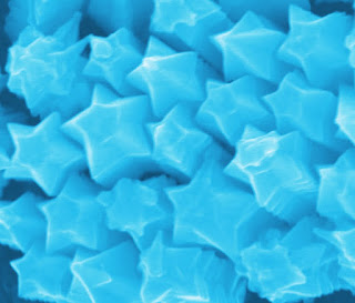
Nanostarfruits begin as gold nanowires with pentagonal cross-sections. Rice chemist Eugene Zubarev believes silver ions and bromide combine to form an insoluble salt that retards particle growth along the pentagons’ flat surfaces. Photo courtesy Zubarev Lab / Rice University.

Gold nanoparticles

Gold nanoparticles created by the Rice University lab of Eugene Zubarev take on the shape of starfruit in a chemical bath with silver nitrate, ascorbic acid and gold chloride. Photo courtesy Zubarev Lab/Rice University
Zubarev and Vigderman grew batches of the star-shaped rods in a chemical bath. They started with seed particles of highly purified gold nanorods with pentagonal cross-sections developed by Zubarev’s lab in 2008 and added them to a mixture of silver nitrate, ascorbic acid and gold chloride.

Over 24 hours, the particles plumped up to 550 nanometers long and 55 nanometers wide, many with pointy ends. The particles take on ridges along their lengths; photographed tip-down with an electron microscope, they look like stacks of star-shaped pillows.

Why the pentagons turn into stars is still a bit of a mystery, Zubarev said, but he was willing to speculate. “For a long time, our group has been interested in size amplification of particles,” he said. “Just add gold chloride and a reducing agent to gold nanoparticles, and they become large enough to be seen with an optical microscope. But in the presence of silver nitrate and bromide ions, things happen differently.”

When Zubarev and Vigderman added a common surfactant, cetyltrimethylammonium bromide (aka CTAB), to the mix, the bromide combined with the silver ions to produce an insoluble salt. “We believe a thin film of silver bromide forms on the side faces of rods and partially blocks them,” Zubarev said.

This in turn slowed down the deposition of gold on those flat surfaces and allowed the nanorods to gather more gold at the pentagon’s points, where they grew into the ridges that gave the rods their star-like cross-section. “Silver bromide is likely to block flat surfaces more efficiently than sharp edges between them,” he said.


The researchers tried replacing silver with other metal ions such as copper, mercury, iron and nickel. All produced relatively smooth nanorods. “Unlike silver, none of these four metals form insoluble bromides, and that may explain why the amplification is highly uniform and leads to particles with smooth surfaces,” he said.

The researchers also grew longer nanowires that, along with their optical advantages, may have unique electronic properties. Ongoing experiments with Stephan Link, an assistant professor of chemistry and chemical and biomolecular engineering, will help characterize the starfruit nanowires’ ability to transmit a plasmonic signal. That could be useful for waveguides and other optoelectronic devices.

But the primary area of interest in Zubarev’s lab is biological. “If we can modify the surface roughness such that biological molecules of interest will adsorb selectively on the surface of our rugged nanorods, then we can start looking at very low concentrations of DNA or cancer biomarkers. There are many cancers where the diagnostics depend on the lowest concentration of the biomarker that can be detected.”

The National Science Foundation and Welch Foundation supported the research.

-30- +sookie tex

Contact: David Ruth david@rice.edu 713-348-6327 Rice University Mike Williams 713-348-6728 mikewilliams@rice.edu

Tuesday, March 27, 2012

Using nanoparticles and magnetic fields cancerous tumor cells killed in half an hour without harming healthy cells VIDEO

Athens, Ga. - Using nanoparticles and alternating magnetic fields, University of Georgia scientists have found that head and neck cancerous tumor cells in mice can be killed in half an hour without harming healthy cells.

The findings, published recently in the journal Theranostics, mark the first time to the researchers' knowledge this cancer type has been treated using magnetic iron oxide nanoparticle-induced hyperthermia, or above-normal body temperatures, in laboratory mice.

"We show that we can use a small concentration of nanoparticles to kill the cancer cells," said Qun Zhao, lead author and assistant professor of physics in the Franklin College of Arts and Sciences. Researchers found that the treatment easily destroyed the cells of cancerous tumors that were composed entirely of a type of tissue that covers the surface of a body, which is also known as epithelium.

Several researchers around the globe are exploring the use of heated nanoparticles as a potential cancer treatment. Previous studies also have shown that high temperatures created by combining magnetic iron oxide nanoparticles with strong alternating magnetic currents can create enough heat to kill tumor cells. Zhao said he is optimistic about his findings, but explained that future studies will need to include larger animals before a human clinical trial could be considered.

For the experiment, researchers injected a tiny amount—a tenth of a teaspoon, or 0.5 milliliter—of nanoparticle solution directly into the tumor site. With the mouse relaxed under anesthesia, they placed the animal in a plastic tube wrapped with a wire coil that generated magnetic fields that alternated directions 100,000 times each second. The magnetic fields produced by the wire coil heated only the concentrated nanoparticles within the cancerous tumor and left the surrounding healthy cells and tissue unharmed.


Zhao said the study paves the way for additional research that might investigate how to use a biodegradable nanoparticle material similar to magnetic iron oxide for other roles in fighting cancer, such as carrying and delivering anti-cancer drugs to the tumor site.

"When the cancer cell is experiencing this heated environment, then it becomes more susceptible to drugs," Zhao said.

Qun Zhao

Magnetic iron oxide nanoparticles could be useful in improving the contrast in magnetic resonance imaging at a cancer site, he said. In other words, the nanoparticles could help physicians detect cancer even if the cancer is not visible to the naked eye with an MRI scan.

"The reason I am interested in using these magnetic nanoparticles is because we hope to one day be able to offer diagnosis and therapeutics, or theranostics, using a single agent," Zhao said.

The research was supported by a National Cancer Institute Head and Neck Specialized Program of Research Excellence at Emory University.

The paper's additional authors are Luning Wang, Rui Cheng, Leidong Mao, Robert Arnold, Simon Platt and Elizabeth W. Howerth, all of UGA, and Zhuo G. Chen of Emory University. +sookie tex

Contact: Qun Zhao qzhao@physast.uga.edu 706-583-5558 University of Georgia

Saturday, March 24, 2012

jellyfish robot to feed off hydrogen and oxygen gases found in water VIDEO

jellyfish robot to feed off hydrogen and oxygen gases found in water VIDEO

Researchers at The University of Texas at Dallas (http://www.utdallas.edu/) and Virginia Tech (http://www.vt.edu/) have created an undersea vehicle inspired by the common jellyfish that runs on renewable energy and could be used in ocean dives for rescue and surveillance missions.

In a study published this week in Smart Materials and Structures (http://iopscience.iop.org/0964-1726/21/4/045013), scientists created a robotic jellyfish, dubbed RoboJelly, to feed off hydrogen and oxygen gases found in water.

“We’ve created an underwater robot that doesn’t need batteries or electricity,” said Dr. Yonas Tadesse, assistant professor of mechanical engineering (http://me.utdallas.edu/index.html) at UT Dallas and lead author of the study. “It feeds off hydrogen and oxygen gasses, and the only waste released as it travels is more water.”

Engineers and scientists have increasingly turned to nature for inspiration when creating new technologies. The simple yet powerful movement of the moon jellyfish made it an appealing animal to simulate.

Contact Information for the DNR: LaKisha Ladson Lakisha.ladson@utdallas.edu 972-883-2155 or 972-883-4183 (office) 469-363-0231 (cell) +sookie tex


UT Dallas Robotic Jellyfish | Length: :30

Thursday, March 22, 2012

Plasmons resonate in quantum-sized metal nanoparticles

Quantum plasmons demonstrated in atomic-scale nanoparticles
Positive identification of plasmons in nano particles could open new engineering possibilities at the nanoscale

The physical phenomenon of plasmon resonances in small metal particles has been used for centuries. They are visible in the vibrant hues of the great stained-glass windows of the world. More recently, plasmon resonances have been used by engineers to develop new, light-activated cancer treatments and to enhance light absorption in photovoltaics and photocatalysis.

"The stained-glass windows of Notre Dame Cathedral and Stanford Chapel derive their color from metal nanoparticles embedded in the glass. When the windows are illuminated, the nanoparticles scatter specific colors depending on the particle's size and geometry " said Jennifer Dionne, an assistant professor of materials science and engineering at Stanford and the senior author of a new paper on plasmon resonances to be published in the journal Nature. In the study, the team of engineers report the direct observation of plasmon resonances of individual metal particles measuring down to one nanometer in diameter—just a few atoms across.

"For particles smaller than about ten nanometers in diameter, plasmon resonances are poorly understood," said Jonathan Scholl, a doctoral candidate in Dionne's lab and first author of the paper. "This class of quantum-sized metal nanoparticles has been largely under-utilized. Exploring their size-dependent nature could open up some interesting applications at the nanoscale."

Longstanding debate

The science of tiny metal particles has perplexed physicists and engineers for decades. Below a certain threshold, as metallic particles near the quantum scale —about 10 nanometers in diameter — classical physics breaks down. The particles begin to demonstrate unique physical and chemical properties that bulk counterparts of the very same materials do not. A nanoparticle of silver measuring a few atoms across, for instance, will respond to photons and electrons in ways profoundly different from a larger particle or slab of silver.

quantum plasmons

San Francisco artist Kate Nichols creates structurally colored artwork using Surface Plasmon Resonances, the same phenomenon described by Scholl and Dionne. This image is a selected view from Nichols's two-part installation at The Leonardo Museum. Nature chose the same image to grace the cover of its issue featuring the Scholl/Koh/Dionne research. Credit: Kate Nichols. Through the Looking Glass 1. Silver nanoparticles on glass. 2011. In situ at The Leonardo Museum, Salt Lake City. Photo: Donald Felton/Almac Camera. www.katenicholsstudio.com

By clearly illustrating the details of this classical-to-quantum transition, Scholl and Dionne have pushed the field of plasmonics into a new realm that could have lasting consequences for catalytic processes such as artificial photosynthesis, cancer research and treatment, and quantum computing.

"Particles at this scale are more sensitive and more reactive than bulk materials," said Dionne. "But we haven't been able to take full advantage of their optical and electronic properties without a complete picture of the science. This paper provides the foundation for new avenues of nanotechnology entering the 100-to-10,000 atom regime."

Noble metals

In recent years, engineers have paid particular attention to nanoparticles of the noble metals: silver, gold, palladium, platinum and so forth. These metals are well known to support localized surface plasmon resonances, the collective oscillations of electrons at the metal surface in response to light or an electric field.

Other important physical properties can be further driven when plasmons are constrained in extremely small spaces, like the nanoparticles Dionne and Scholl studied. The phenomenon is known as quantum confinement.

Depending on the shape and size of the particle, quantum confinement can dominate a particle's electronic and optical response. This research allows scientists, for the first time, to directly correlate a quantum-sized plasmonic particle's geometry—its shape and size—with its plasmon resonances.

Standing to benefit

Nanotechnology stands to benefit from this new understanding. "We might discover novel electronic or photonic devices based on excitation and detection of plasmons in quantum-sized particles. Alternatively, there could be opportunities in catalysis, quantum optics, and bio-imaging and therapeutics," said Dionne.

Medical science, for instance, has devised a way to use nanoparticles excited by light to burn away cancer cells, a process known as photothermal ablation. Metal nanoparticles are affixed with molecular appendages called ligands that attach exclusively to chemical receptors on cancerous cells. When irradiated with infrared light, the metal nanoparticles heat up, burning away the cancerous cells while leaving the surrounding healthy tissue unaffected. The properties of smaller nanoparticles might improve the accuracy and the effectiveness of such technologies, particularly since they can be more easily integrated into cells.

There is great promise for such small nanoparticles in catalysis, as well. The greater surface-area-to-volume ratios offered by atomic-scale nanoparticles could improve water-splitting and artificial photosynthesis, yielding clean and renewable energy sources from artificial fuels. Taking advantage of quantum plasmons in these metallic nanoparticles could significantly improve catalyic rates and efficiencies.

Aiding and abetting

The researchers' ability to observe plasmons in particles of such small size was abetted by the powerful, multi-million dollar environmental scanning transmission electron microscope (E-STEM) installed recently at Stanford's Center for Nanoscale Science and Engineering, one of just a handful of such microscopes in the world.

E-STEM imaging was used in conjunction with electron energy-loss spectroscopy (EELS) — a research technique that measures the change of an electron's energy as it passes through a material — to determine the shape and behavior of individual nanoparticles. Combined, STEM and EELS allowed the team to address many of the ambiguities of previous investigations.

"With the new microscope, we can resolve individual atoms within the nanoparticle," said Dionne, "and we can directly observe these particles' quantum plasmon resonances."

Ai Leen Koh, a research scientist at the Stanford Nanocharacterization Laboratory, and co-author of the paper, noted: "Even though plasmons can be probed using both light and electrons, electron excitation is advantageous in that it allows us to image the nanoparticle down to the atomic level and study its plasmon resonances at the same time."

Scholl added, "Someday, we might use the technique to watch reactions in progress to better understand and optimize them."

Elegant and versatile

The researchers concluded by explaining the physics of their discovery through an elegant and versatile analytical model based on well-known quantum mechanical principles.

"Technically speaking, we've created a relatively simple, computationally light model that describes plasmonic systems where classical theories have failed," said Scholl.

Their elegant and versatile model opens up numerous opportunities for scientific gain.

"This paper represents fundamental research. We have clarified what was an ambiguous scientific understanding and, for the first time, directly correlated a particle's geometry with its plasmonic resonance for quantum-sized particles," summarized Dionne. "And this could have some very interesting, and very promising, implications and applications."

### +sookie tex

This research was made possible by the National Science Foundation Graduate Research Fellowship Program, the Stanford Terman Fellowship and the Robert N. Noyce Family Faculty Fellowship.

This article was written by Andrew Myers is associate director of communications for the Stanford School of Engineering.

Contact: Andrew Myers admyers@stanford.edu 650-736-2245 Stanford School of Engineering

Tuesday, March 20, 2012

Berkeley Lab Improving Organic and Molecular Electronic Devices

Better Organic Electronics, Berkeley Lab Researchers Show the Way Forward for Improving Organic and Molecular Electronic Devices.

Future prospects for superior new organic electronic devices are brighter now thanks to a new study by researchers with the U.S. Department of Energy (DOE)’s Lawrence Berkeley National Laboratory (Berkeley Lab). Working at the Lab’s Molecular Foundry, a DOE nanoscience center, the team has provided the first experimental determination of the pathways by which electrical charge is transported from molecule-to-molecule in an organic thin film. Their results also show how such organic films can be chemically modified to improve conductance.

“We have shown that when the molecules in organic thin films are aligned in particular directions, there is much better conductance,” says Miquel Salmeron, a leading authority on nanoscale surface imaging who directs Berkeley Lab’s Materials Sciences Division and who led this study. “Chemists already know how to fabricate organic thin films in a way that can achieve such an alignment, which means they should be able to use the information provided by our methodology to determine the molecular alignment and its role on charge transport across and along the molecules. This will help improve the performances of future organic electronic devices.”

Salmeron and Shaul Aloni, also of the Materials Sciences Division, are the corresponding authors of a paper in the journal NanoLetters that describes this work. The paper is titled “Electron Microscopy Reveals Structure and Morphology of One Molecule Thin Organic Films.” Other co-authors were Virginia Altoe, Florent Martin and Allard Katan.

organic thin film deposited on a silicon nitride membrane

Scanning transmission electron microscopy image of an organic thin film deposited on a silicon nitride membrane. Yellow arrows indicate the lattice orientation of each crystalline domain. Green circles mark polycrystalline areas. (Image from Berkeley Lab’s Molecular Foundry)

monolayer organic thin films

Electron diffraction patterns provide a wealth of information about the morphology, structure, and quality of monolayer organic thin films. (Image from Berkeley Lab’s Molecular Foundry
Organic electronics, also known as plastic or polymer electronics, are devices that utilize carbon-based molecules as conductors rather than metals or semiconductors. They are prized for their low costs, light weight and rubbery flexibility. Organic electronics are also expected to play a big role in molecular computing, but to date their use has been hampered by low electrical conductance in comparison to metals and semiconductors.

“Chemists and engineers have been using their intuition and trial-and-error testing to make progress in the field but at some point you hit a wall unless you understand what is going on at the molecular level, for example, how electrons or holes flow through or across molecules, how the charge transport depends on the structure of the organic layers and the orientation of the molecules, and how the charge transport responds to mechanical forces and chemical inputs,” Salmeron says. “With our experimental results, we have shown that we can now provide answers for these questions.”

In this study, Salmeron and his colleagues used electron diffraction patterns to map the crystal structures of molecular films made from monolayers of short versions of commonly used polymers containing long chains of thiophene units. They focused specifically on pentathiophene butyric acid (5TBA) and two of its derivatives (D5TBA and DH5TBA) that were induced to self-assemble on various electron-transparent substrates. Pentathiophenes – molecules containing a ring of four carbon and one sulfur atoms – are members of a well-studied and promising family of organic semiconductors.

Obtaining structural crystallographic maps of monolayer organic films using electron beams posed a major challenge, as Aloni explains.

“These organic molecules are extremely sensitive to high energy electrons,” he says. “When you shoot a beam of high energy electrons through the film it immediately affects the molecules. Within few seconds we no longer see the signature intermolecular alignment of the diffraction pattern.

Despite this, when applied correctly, electron microscopy becomes essential tool that can provide unique information on organic samples.”

Salmeron, Aloni and their colleagues overcame the challenge through the combination of a unique strategy they developed and a transmission electron microscope (TEM) at the Molecular Foundry’s Imaging and Manipulation of Nanostructures Facility. Electron diffraction patterns were collected as a parallel electron beam was scanned over the film, then analyzed by computer to generate structural crystallographic maps.

“These maps contain uncompromised information of the size, symmetry and orientation of the unit cell, the orientation and structure of the domains, the degree of crystallinity, and any variations on the micrometer scale,” says first author Altoe. “Such data are crucial to understanding the structure and electrical transport properties of the organic films, and allow us to track small changes driven by chemical modifications of the support films.”

In their paper, the authors acknowledge that to gain structural information they had to sacrifice some resolution.

“The achievable resolution of the structural map is a compromise between sample radiation hardness, detector sensitivity and noise, and data acquisition rate,” Salmeron says. “To keep the dose of high energy electrons at a level the monolayer film could support and still be able to collect valuable information about its structure, we had to spread the beam to a 90 nanometer diameter. However a fast and direct control of the beam position combined with the use of fast and ultrasensitive detectors should allow for the use of smaller beams with a higher electron flux, resulting in a better than 10 nanometer resolution.”

While the combination of organic molecular films and substrates in this study conduct electrical current via electron holes (positively-charged energy spaces), Salmeron and his colleagues say their structural mapping can also be applied to materials whose conductance is electron-based.

“We expect our methodology to have widespread applications in materials research,” Salmeron says.

Aloni and Altoe say this methodology is now available at the Imaging and Manipulation of Nanostructures Facility for users of the Molecular Foundry.

This research was supported by the DOE Office of Science.

# # # +sookie tex

Lawrence Berkeley National Laboratory addresses the world’s most urgent scientific challenges by advancing sustainable energy, protecting human health, creating new materials, and revealing the origin and fate of the universe. Founded in 1931, Berkeley Lab’s scientific expertise has been recognized with 13 Nobel prizes. The University of California manages Berkeley Lab for the U.S. Department of Energy’s Office of Science. For more, visit www.lbl.gov.

The Molecular Foundry is one of five DOE Nanoscale Science Research Centers (NSRCs), national user facilities for interdisciplinary research at the nanoscale, supported by the DOE Office of Science. Together the NSRCs comprise a suite of complementary facilities that provide researchers with state-of-the-art capabilities to fabricate, process, characterize and model nanoscale materials, and constitute the largest infrastructure investment of the National Nanotechnology Initiative. The NSRCs are located at DOE’s Argonne, Brookhaven, Lawrence Berkeley, Oak Ridge and Sandia and Los Alamos National Laboratories. For more information about the DOE NSRCs, please visit science.energy.gov.

TEXT and IMAGE: Lynn Yarris (510) 486-5375 lcyarris@lbl.gov

Sunday, March 18, 2012

Cost effective and highly active palladium and gold based catalysts for hydrogen fuel cells

Hydrogen fuel cells, like those found in some "green" vehicles, have a lot of promise as an alternative fuel source, but making them practical on a large scale requires them to be more efficient and cost effective.

A research team from the University of Central Florida may have found a way around both hurdles.

The majority of hydrogen fuel cells use catalysts made of a rare and expensive metal – platinum. There are few alternatives because most elements can't endure the fuel cell's highly acidic solvents present in the reaction that converts hydrogen's chemical energy into electrical power. Only four elements can resist the corrosive process – platinum, iridium, gold and palladium. The first two are rare and expensive, which makes them impractical for large-scale use. The other two don't do well with the chemical reaction.

UCF Professor Sergey Stolbov and postdoctoral research associate Marisol Alcántara Ortigoza focused on making gold and palladium better suited for the reaction.

They created a sandwich-like structure that layers cheaper and more abundant elements with gold and palladium and other elements to make it more effective.

The outer monoatomic layer (the top of the sandwich) is either palladium or gold. Below it is a layer that works to enhance the energy conversion rate but also acts to protect the catalyst from the acidic environment. These two layers reside on the bottom slice of the sandwich -- an inexpensive substrate (tungsten), which also plays a role in the stability of the catalyst.

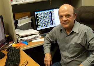
Sergey Stolbov, University of Central Florida

Caption: Sergey Stolbov works in his lab at UCF. Credit: UCF. Usage Restrictions: None.
"We are very encouraged by our first attempts that suggest that we can create two cost-effective and highly active palladium- and gold-based catalysts –for hydrogen fuel cells, a clean and renewable energy source," Stolbov said.

Stolbov's work was recently published in The Journal of Physical Chemistry Letters.

By creating these structures, more energy is converted, and because the more expensive and rare metals are not used, the cost could be significantly less.

Stolbov said experiments are needed to test their predictions, but he says the approach is quite reliable. He's already working with a group within the U.S. Department of Energy to determine whether the results can be duplicated and have potential for large-scale application.

If a way could be found to make hydrogen fuel cells practical and cost effective, vehicles that run on gasoline and contribute to the destruction of the ozone layer could become a thing of the past.

Stolbov joined UCF's physics department in 2006. Before that he was a research assistant professor at Kansas State University. He earned multiple degrees in physics from Rostov State University in Russia and was a Postdoctoral Fellow at the Carnegie Institution of Washington, D.C. He is a frequent international speaker and has written dozens of articles on physics.

### +sookie tex

UCF Stands For Opportunity --The University of Central Florida is a metropolitan research university that ranks as the second largest in the nation with more than 58,000 students. UCF's first classes were offered in 1968. The university offers impressive academic and research environments that power the region's economic development. UCF's culture of opportunity is driven by our diversity, Orlando environment, history of entrepreneurship and our youth, relevance and energy. For more information visit news.ucf.edu

Contact: Zenaida Gonzalez Kotala zenaida.kotala@ucf.edu 407-823-6120 University of Central Florida

Friday, March 16, 2012

Lithium atoms adhered to a graphene lattice that will produce electricity when bent, squeezed or twisted

By depositing atoms on one side of a grid of the “miracle material” graphene, researchers at Stanford have engineered piezoelectricity into a nanoscale material for the first time. The implications could yield dramatic degree of control in nanotechnology.

By Andrew Myers

In what became known as the ‘Scotch tape technique,” researchers first extracted graphene with a piece of adhesive in 2004. Graphene is a single layer of carbon atoms arranged in a honeycomb, hexagonal pattern. It looks like chicken wire.

Graphene is a wonder material. It is a one-hundred-times-better conductor of electricity than silicon. It is stronger than diamond. And, at just one atom thick, it is so thin as to be essentially a two-dimensional material. Such promising physics have made graphene the most studied substance of the last decade, particularly in nanotechnology. In 2010, the researchers who first isolated it shared the Nobel Prize.

Yet, while graphene is many things, it is not piezoelectric. Piezoelectricity is the property of some materials to produce electric charge when bent, squeezed or twisted. Perhaps more importantly, piezoelectricity is reversible. When an electric field is applied, piezoelectric materials change shape, yielding a remarkable level of engineering control.

Piezoelectrics have found application in countless devices from watches, radios and ultrasound to the push-button starters on propane grills, but these uses all require relatively large, three-dimensional quantities of piezoelectric materials.

Piezoelectric graphene

This illustration shows lithium atoms (red) adhered to a graphene lattice that will produce electricity when bent, squeezed or twisted. Conversely, the graphene will deform when an electric field is applied, opening new possibilities in nanotechnology. Illustration: Mitchell Ong, Stanford School of Engineering

Now, in a paper published in the journal ACS Nano, two materials engineers at Stanford have described how they have engineered piezoelectrics into graphene, extending for the first time such fine physical control to the nanoscale.
Straintronics

“The physical deformations we can create are directly proportional to the electrical field applied. This represents a fundamentally new way to control electronics at the nanoscale,” said Evan Reed, head of the Materials Computation and Theory Group at Stanford and senior author of the study.

This phenomenon brings new dimension to the concept of ‘straintronics,’ he said, because of the way the electrical field strains—or deforms—the lattice of carbon, causing it to change shape in predictable ways.

“Piezoelectric graphene could provide an unparalleled degree of electrical, optical or mechanical control for applications ranging from touchscreens to nanoscale transistors,” said Mitchell Ong, a post-doctoral scholar in Reed’s lab and first author of the paper.

Using a sophisticated modeling application running on high-performance supercomputers, the engineers simulated the deposition of atoms on one side of a graphene lattice — a process known as doping — and measured the piezoelectric effect.

They modeled graphene doped with lithium, hydrogen, potassium and fluorine, as well as combinations of hydrogen and fluorine and lithium and fluorine on either side of the lattice. Doping just one side of the graphene, or doping both sides with different atoms, is key to the process as it breaks graphene’s perfect physical symmetry, which otherwise cancels the piezoelectric effect.

The results surprised both engineers.

“We thought the piezoelectric effect would be present, but relatively small. Yet, we were able to achieve piezoelectric levels comparable to traditional three-dimensional materials,” said Reed. “It was pretty significant.”

Designer piezoelectricity

The researchers were further able to fine tune the effect by pattern doping the graphene—selectively placing atoms in specific sections and not others.

“We call it designer piezoelectricity because it allows us to strategically control where, when and how much the graphene is deformed by an applied electrical field with promising implications for engineering," said Ong.

While the results in creating piezoelectric graphene are encouraging, the researchers believe that their technique might further be used to engineer piezoelectricity in nanotubes and other nanomaterials with applications ranging from electronics, photonics, and energy harvesting to chemical sensing and high-frequency acoustics.

“We’re already looking at new piezoelectric devices based on other 2D and low-dimensional materials, hoping they might open new and dramatic possibilities in nanotechnology,” said Reed.

The Army High Performance Computing Research Center at Stanford University and the National Energy Research Scientific Computing Center (NERSC) at the Lawrence Berkeley National Laboratory supported this research.

Listen to Reed and Ong talk about their work with ACS Nano: http://www.stanford.edu/group/evanreed/media/ancac3-0212.mp3

Andrew Myers is the associate director of communications for the Stanford University School of Engineering. +sookie tex

Media Contacts

Andrew Myers Associate Director of Communications 650.736.2245 admyers@stanford.edu Jamie Beckett Director of Communications and Alumni Relations 650.736.2241 jbeckett@stanford.edu

Thursday, March 15, 2012

Graphene supercapacitor holding promise for a significant advance in energy storage technology

Electrochemical capacitors (ECs), also known as supercapacitors or ultracapacitors, differ from regular capacitors that you would find in your TV or computer in that they store substantially higher amounts of charges. They have garnered attention as energy storage devices as they charge and discharge faster than batteries, yet they are still limited by low energy densities, only a fraction of the energy density of batteries. An EC that combines the power performance of capacitors with the high energy density of batteries would represent a significant advance in energy storage technology. This requires new electrodes that not only maintain high conductivity but also provide higher and more accessible surface area than conventional ECs that use activated carbon electrodes.

Now researchers at UCLA have used a standard LightScribe DVD optical drive to produce such electrodes. The electrodes are composed of an expanded network of graphene — a one-atom-thick layer of graphitic carbon — that shows excellent mechanical and electrical properties as well as exceptionally high surface area.

UCLA researchers from the Department of Chemistry and Biochemistry, the Department of Materials Science and Engineering, and the California NanoSystems Institute demonstrate high-performance graphene-based electrochemical capacitors that maintain excellent electrochemical attributes under high mechanical stress. The paper is published in the journal Science.

The process is based on coating a DVD disc with a film of graphite oxide that is then laser treated inside a LightScribe DVD drive to produce graphene electrodes. Typically, the performance of energy storage devices is evaluated by two main figures, the energy density and power density. Suppose we are using the device to run an electric car — the energy density tells us how far the car can go a single charge whereas the power density tells us how fast the car can go. Here, devices made with Laser Scribed Graphene (LSG) electrodes exhibit ultrahigh energy density values in different electrolytes while maintaining the high power density and excellent cycle stability of ECs. Moreover, these ECs maintain excellent electrochemical attributes under high mechanical stress and thus hold promise for high power, flexible electronics.

Graphene Supercapacitors

Graphene Supercapacitors, Schematic showing the structure of laser scribed graphene supercapacitors.
"Our study demonstrates that our new graphene-based supercapacitors store as much charge as conventional batteries, but can be charged and discharged a hundred to a thousand times faster," said Richard B. Kaner, professor of chemistry & materials science and engineering.

"Here, we present a strategy for the production of high-performance graphene-based ECs through a simple all solid-state approach that avoids the restacking of graphene sheets," said Maher F. El-Kady, the lead author of the study and a graduate student in Kaner's lab.

The research team has fabricated LSG electrodes that do not have the problems of activated carbon electrodes that have so far limited the performance of commercial ECs. First, The LightScribe laser causes the simultaneous reduction and exfoliation of graphite oxide and produces an open network of LSG with substantially higher and more accessible surface area. This results in a sizable charge storage capacity for the LSG supercapacitors. The open network structure of the electrodes helps minimize the diffusion path of electrolyte ions, which is crucial for charging the device. This can be accounted for by the easily accessible flat graphene sheets, whereas most of the surface area of activated carbon resides in very small pores that limit the diffusion of ions. This means that LSG supercapacitors have the ability to deliver ultrahigh power in a short period of time whereas activated carbon cannot.

Additionally, LSG electrodes are mechanically robust and show high conductivity (>1700 S/m) compared to activated carbons (10-100 S/m). This means that LSG electrodes can be directly used as supercapacitor electrodes without the need for binders or current collectors as is the case for conventional activated carbon ECs. Furthermore, these properties allow LSG to act as both the active material and current collector in the EC. The combination of both functions in a single layer leads to a simplified architecture and makes LSG supercapacitors cost-effective devices.

Commercially available ECs consist of a separator sandwiched between two electrodes with liquid electrolyte that is either spirally wound and packaged into a cylindrical container or stacked into a button cell. Unfortunately, these device architectures not only suffer from possible harmful leakage of electrolytes, but their design makes it difficult to use them for practical flexible electronics.

The research team replaced the liquid electrolyte with a polymer gelled electrolyte that also acts as a separator, further reducing the device thickness and weight and simplifying the fabrication process as it does not require special packaging materials.

In order to evaluate under real conditions the potential of this all solid-state LSG-EC for flexible storage, the research team placed a device under constant mechanical stress to analyze its performance. Interestingly enough, this had almost no effect on the performance of the device.

"We attribute the high performance and durability to the high mechanical flexibility of the electrodes along with the interpenetrating network structure between the LSG electrodes and the gelled electrolyte," explains Kaner. "The electrolyte solidifies during the device assembly and acts like glue that holds the device components together."

The method improves the mechanical integrity and increases the life cycle of the device even when tested under extreme conditions.

Since this remarkable performance has yet to be realized in commercial devices, these LSG supercapacitors could lead the way to ideal energy storage systems for next generation flexible, portable electronics.

###

The California NanoSystems Institute is an integrated research facility located at UCLA and UC Santa Barbara. Its mission is to foster interdisciplinary collaborations in nanoscience and nanotechnology; to train a new generation of scientists, educators and technology leaders; to generate partnerships with industry; and to contribute to the economic development and the social well-being of California, the United States and the world. The CNSI was established in 2000 with $100 million from the state of California. The total amount of research funding in nanoscience and nanotechnology awarded to CNSI members has risen to over $900 million.

UCLA CNSI members are drawn from UCLA's College of Letters and Science, the David Geffen School of Medicine, the School of Dentistry, the School of Public Health and the Henry Samueli School of Engineering and Applied Science. They are engaged in measuring, modifying and manipulating atoms and molecules — the building blocks of our world. Their work is carried out in an integrated laboratory environment. This dynamic research setting has enhanced understanding of phenomena at the nanoscale and promises to produce important discoveries in health, energy, the environment and information technology. +sookie tex

Contact: Jennifer Marcus jmarcus@cnsi.ucla.edu 310-267-4839 University of California - Los Angeles

Tuesday, March 13, 2012

Graphene rock star of materials science has an Achilles heel: It is exceptionally sensitive to its electrical environment

These days, graphene is the rock star of materials science, but it has an Achilles heel: It is exceptionally sensitive to its electrical environment.

This single-atom-thick honeycomb of carbon atoms is lighter than aluminum, stronger than steel and conducts heat and electricity better than copper. As a result, scientists around the world are trying to turn it into better computer displays, solar panels, touch screens, integrated circuits and biomedical sensors, among other possible applications. However, it has proven extremely difficult to reliably create graphene-based devices that live up to its electrical potential when operating at room temperature and pressure.

Now, writing in the Mar. 13 issue of the journal Nature Communications, a team of Vanderbilt physicists reports that they have nailed down the source of the interference inhibiting the rapid flow of electrons through graphene-based devices and found a way to suppress it. This discovery allowed them to achieve record-levels of room-temperature electron mobility – the measure of the speed that electrons travel through a material – three times greater than those reported in previous graphene-based devices.

According to the experts, graphene may have the highest electron mobility of any known material. In practice, however, the measured levels of mobility, while significantly higher than in other materials like silicon, have been considerably below its potential.

“The problem is that, when you make graphene, you don’t get just graphene. You also get a lot of other stuff,” said Kirill Bolotin, assistant professor of physics, who conducted the study with research associate A.K.M. Newaz. “Graphene is extraordinarily susceptible to external influences so the electrical fields created by charged impurities on its surface scatter the electrons traveling through the graphene sheets, making graphene-based transistors operate slower and heat up more.”

graphene device

An image of a suspended graphene device made by a scanning probe microscope. The graphene sheet is the orange-colored layer suspended between six rectangular columns made of silicon dioxide and capped by gold. (A.K.M. Newaz / Bolotin Lab)
A number of researchers had proposed that the charged impurities that are omnipresent on the surface of graphene were the main culprits, but they were not completely certain. Also, several other theories had been advanced to explain the phenomenon.

“Our study shows without question that the charged stuff is the problem and, if you want to make better graphene devices, it is the enemy that you need to fight,” Bolotin said.

At the same time, the experiment didn’t find evidence supporting one of the alternative theories, that ripples in the graphene sheets were a significant source of electron scattering

In order to get a handle on the mobility problem, Bolotin’s team suspended sheets of graphene in a series of different liquids and measured the material’s electric transport properties. They found that graphene’s electron mobility is dramatically increased when graphene is submerged in electrically neutral liquids that can absorb large amounts of electrical energy (have large dielectric constants). They achieved the record-level mobility of 60,000 using anisole, a colorless liquid with a pleasant, aromatic odor used chiefly in perfumery.

“These liquids suppress the electrical fields from the impurities, allowing the electrons to flow with fewer obstructions,” Bolotin said.

Now that the source of the degradation in electrical performance of graphene has been clearly identified, it should be possible to come up with reliable device designs, Bolotin said.

According to the physicist, there is also a potential advantage to graphene’s extraordinary sensitivity to its environment that can be exploited. It should make extremely sensitive sensors of various types and, because it is made entirely of carbon, it is biocompatible and so should be ideal for biological sensors.

University Distinguished Professor of Physics and Engineering Sokrates Pantelides and research associates Yevgeniy Puzyrev and Bin Wang contributed to the study.

The research was funded by an award from the National Science Foundation. +sookie tex

Contact: David Salisbury, (615) 322-NEWS david.salisbury@vanderbilt.edu

Saturday, March 10, 2012

Carbon nanotubes to increase the speed of biological sensors

CORVALLIS, Ore. – Researchers at Oregon State University have tapped into the extraordinary power of carbon “nanotubes” to increase the speed of biological sensors, a technology that might one day allow a doctor to routinely perform lab tests in minutes, speeding diagnosis and treatment while reducing costs.

The new findings have almost tripled the speed of prototype nano-biosensors, and should find applications not only in medicine but in toxicology, environmental monitoring, new drug development and other fields.

The research was just reported in Lab on a Chip, a professional journal. More refinements are necessary before the systems are ready for commercial production, scientists say, but they hold great potential.

“With these types of sensors, it should be possible to do many medical lab tests in minutes, allowing the doctor to make a diagnosis during a single office visit,” said Ethan Minot, an OSU assistant professor of physics. “Many existing tests take days, cost quite a bit and require trained laboratory technicians.

“This approach should accomplish the same thing with a hand-held sensor, and might cut the cost of an existing $50 lab test to about $1,” he said.

The key to the new technology, the researchers say, is the unusual capability of carbon nanotubes. An outgrowth of nanotechnology, which deals with extraordinarily small particles near the molecular level, these nanotubes are long, hollow structures that have unique mechanical, optical and electronic properties, and are finding many applications.

Nanotube sensor

Nanotube sensor

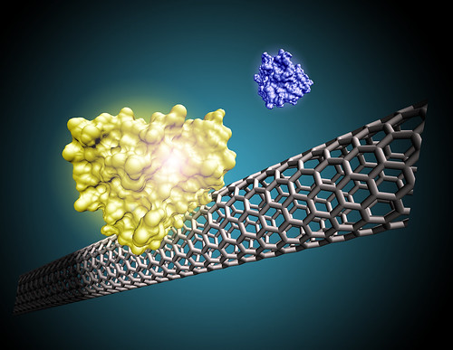
A carbon nanotube treated with a capture agent, in yellow, can bind with and detect the purple-colored target protein - this changes the electrical resistance of the nanotube and creates a sensing device. (Graphic courtesy of Oregon State University)
In this case, carbon nanotubes can be used to detect a protein on the surface of a sensor. The nanotubes change their electrical resistance when a protein lands on them, and the extent of this change can be measured to determine the presence of a particular protein – such as serum and ductal protein biomarkers that may be indicators of breast cancer.

The newest advance was the creation of a way to keep proteins from sticking to other surfaces, like fluid sticking to the wall of a pipe. By finding a way to essentially “grease the pipe,” OSU researchers were able to speed the sensing process by 2.5 times.

Further work is needed to improve the selective binding of proteins, the scientists said, before it is ready to develop into commercial biosensors.

“Electronic detection of blood-borne biomarker proteins offers the exciting possibility of point-of-care medical diagnostics,” the researchers wrote in their study.

“Ideally such electronic biosensor devices would be low-cost and would quantify multiple biomarkers within a few minutes.”

This work was a collaboration of researchers in the OSU Department of Physics, Department of Chemistry, and the University of California at Santa Barbara. A co-author was Vincent Remcho, professor and interim dean of the OSU College of Science, and a national expert in new biosensing technology.

The research was supported by the U.S. Army Research Laboratory through the Oregon Nanoscience and Microtechnologies Institute.
About the OSU College of Science: As one of the largest academic units at OSU, the College of Science has 14 departments and programs, 13 pre-professional programs, and provides the basic science courses essential to the education of every OSU student. Its faculty are international leaders in scientific research.

Contact: Ethan Minot minote@physics.oregonstate.edu 541-737-9671 Oregon State University

Thursday, March 08, 2012

Nanoscale metal lithography into three dimensions with femtosecond laser

Cambridge, Mass. - March 8, 2012 - Researchers in applied physics have cleared an important hurdle in the development of advanced materials, called metamaterials, that bend light in unusual ways.

Working at a scale applicable to infrared light, the Harvard team has used extremely short and powerful laser pulses to create three-dimensional patterns of tiny silver dots within a material. Those suspended metal dots are essential for building futuristic devices like invisibility cloaks.

The new fabrication process, described in the journal Applied Physics Letters, advances nanoscale metal lithography into three dimensions—and does it at a resolution high enough to be practical for metamaterials.

"If you want a bulk metamaterial for visible and infrared light, you need to embed particles of silver or gold inside a dielectric, and you need to do it in 3D, with high resolution," says lead author Kevin Vora, a graduate student at the Harvard School of Engineering and Applied Sciences (SEAS).

"This work demonstrates that we can create silver dots that are disconnected in x, y, and z," Vora says. "There’s no other technique that feasibly allows you to do that. Being able to make patterns of nanostructures in 3D is a very big step towards the goal of making bulk metamaterials."

Vora works in the laboratory of Eric Mazur, Balkanski Professor of Physics and Applied Physics at SEAS. For decades, Mazur has been using a piece of equipment called a femtosecond laser to investigate how very tightly focused, powerful bursts of light can change the electrical, optical, and physical properties of a material.

femtosecond lasers

The experimental setup in Prof. Eric Mazur's laser laboratory at Harvard. Using femtosecond lasers, Mazur and colleagues have developed a new nanofabrication process for use in creating metamaterials.

polymer matrix

A new laser fabrication technique developed at Harvard allows for the creation of precisely arranged silver nanoparticles that are disconnected in 3D and supported by a polymer matrix. The new technique may prove critical in the development of metamaterials. Image courtesy of Kevin Vora.
When a conventional laser shines on a transparent material, the light passes straight through, with slight refraction. The femtosecond laser is special because it emits a burst of photons as bright as the surface of the sun in a flash lasting only 50 quadrillionths (5 × 10-14) of a second. Instead of shining through the material, that energy gets trapped within it, exciting the electrons within the material and achieving a phenomenon known as nonlinear absorption.

Inside the pocket where that energy is trapped, a chemical reaction can take place, permanently altering the internal structure of the material. The process has previously been exploited for 2D and simple 3D metal nanofabrication.

"Normally, when people use femtosecond lasers in fabrication, they’re creating a wood pile structure: something stacked on something else, being supported by something else," explains Mazur.

"If you want to make an array of silver dots, however, they can’t float in space."

In the new process, Vora, Mazur, and their colleagues combine silver nitrate, water, and a polymer called PVP into a solution, which they bake onto a glass slide. The solid polymer then contains ions of silver, which are photoreduced by the tightly focused laser pulses to form nanocrystals of silver metal, supported by the polymer matrix.

The need for this particular combination of chemicals, at the right concentrations, was not obvious in prior work. Researchers sometimes combine silver nitrate with water in order to create silver nanostructures, but that process provides no structural support for a 3D pattern. Another process combines silver nitrate, water, PVP, and ethanol, but the samples darken and degrade very quickly by producing silver crystals throughout the polymer.

With ethanol, the reaction happens too quickly and uncontrollably. Mazur's team needed nanoscale crystals, precisely distributed and isolated in 3D.

"It was just a question of removing that reagent, and we got lucky," Vora says. "What was most surprising about it was how simple it is. It was a matter of using less."

SeungYeon Kang, a graduate student at SEAS, and Shobha Shukla, a former postdoctoral fellow, coauthored the paper. The work was supported by the Air Force Office of Scientific Research.


Contact: Caroline Perry cperry@seas.harvard.edu WEB: Harvard University

Wednesday, March 07, 2012

Nanowire trees to cleanly capture solar energy and harvest it for hydrogen fuel generation

Nanotrees harvest the sun's energy to turn water into hydrogen fuel, Researchers focused on artificial photosynthesis,

University of California, San Diego electrical engineers are building a forest of tiny nanowire trees in order to cleanly capture solar energy without using fossil fuels and harvest it for hydrogen fuel generation. Reporting in the journal Nanoscale, the team said nanowires, which are made from abundant natural materials like silicon and zinc oxide, also offer a cheap way to deliver hydrogen fuel on a mass scale.

"This is a clean way to generate clean fuel," said Deli Wang, professor in the Department of Electrical and Computer Engineering at the UC San Diego Jacobs School of Engineering.

The trees' vertical structure and branches are keys to capturing the maximum amount of solar energy, according to Wang. That's because the vertical structure of trees grabs and adsorbs light while flat surfaces simply reflect it, Wang said, adding that it is also similar to retinal photoreceptor cells in the human eye. In images of Earth from space, light reflects off of flat surfaces such as the ocean or deserts, while forests appear darker.

Wang's team has mimicked this structure in their "3D branched nanowire array" which uses a process called photoelectrochemical water-splitting to produce hydrogen gas. Water splitting refers to the process of separating water into oxygen and hydrogen in order to extract hydrogen gas to be used as fuel. This process uses clean energy with no green-house gas byproduct. By comparison, the current conventional way of producing hydrogen relies on electricity from fossil fuels.

light trapping effect in nanowire arrays

Caption: Schematic shows the light trapping effect in nanowire arrays. Photons on are bounced between single nanowires and eventually absorbed by them (R). By harvesting more sun light using the vertical nanotree structure, Wang’s team has developed a way to produce more hydrogen fuel efficiently compared to planar counterparts where they are reflected off the surface (L).

Credit: Image Credit: Wang Research Group, UC San Diego Jacobs School of Engineering. Originally published in the journal Nanoscale, reproduced by permission of The Royal Society of Chemistry. Usage Restrictions: with full credit.

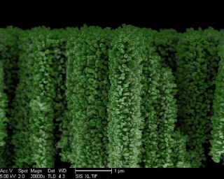
Nanoforest

Caption: This is an electronic microscopic image of a nanoforest, or "3-D branched nanowire array." (Green tint added for contrast.)

Credit: Image Credit: Wang Research Group, UC San Diego Jacobs School of Engineering. Usage Restrictions: with full credit.
"Hydrogen is considered to be clean fuel compared to fossil fuel because there is no carbon emission, but the hydrogen currently used is not generated cleanly," said Ke Sun, a PhD student in electrical engineering who led the project.

By harvesting more sun light using the vertical nanotree structure, Wang's team has developed a way to produce more hydrogen fuel efficiently compared to planar counterparts. Wang is also affiliated with the California Institute of Telecommunications and Information Technology and the Materials Science and Engineering Program at UC San Diego.

The vertical branch structure also maximizes hydrogen gas output, said Sun. For example, on the flat wide surface of a pot of boiling water, bubbles must become large to come to the surface. In the nanotree structure, very small gas bubbles of hydrogen can be extracted much faster. "Moreover, with this structure, we have enhanced, by at least 400,000 times, the surface area for chemical reactions," said Sun.

In the long run, what Wang's team is aiming for is even bigger: artificial photosynthesis. In photosynthesis, as plants absorb sunlight they also collect carbon dioxide (CO2) and water from the atmosphere to create carbohydrates to fuel their own growth. Wang's team hopes to mimic this process to also capture CO2 from the atmosphere, reducing carbon emissions, and convert it into hydrocarbon fuel.

"We are trying to mimic what the plant does to convert sunlight to energy," said Sun. "We are hoping in the near future our 'nanotree' structure can eventually be part of an efficient device that functions like a real tree for photosynthesis."

###

The team is also studying alternatives to zinc oxide, which absorbs the sun's ultraviolet light, but has stability issues that affect the lifetime usage of the nanotree structure. Students with the Wang Research Group will be presenting this research on April 12, 2012, at Research Expo, the annual research and networking event of the UC San Diego Jacobs School of Engineering. Register for Research Expo.

Contact: Catherine Hockmuth chockmuth@ucsd.edu 858-822-1359 University of California - San Diego

Monday, March 05, 2012

Superthin “nanoglue” that could be used in new-generation microchip fabrication

Engineers at the University of California, Davis, have invented a superthin “nanoglue” that could be used in new-generation microchip fabrication.

“The material itself (say, semiconductor wafers) would break before the glue peels off,” said Tingrui Pan, professor of biomedical engineering. He and his fellow researchers have filed a provisional patent.

Conventional glues form a thick layer between two surfaces. Pan’s nanoglue, which conducts heat and can be printed, or applied, in patterns, forms a layer the thickness of only a few molecules.

The nanoglue is based on a transparent, flexible material called polydimethylsiloxane, or PDMS, which, when peeled off a smooth surface usually leaves behind an ultrathin, sticky residue that researchers had mostly regarded as a nuisance.

Pan and his colleagues realized that this residue could instead be used as glue, and enhanced its bonding properties by treating the residue surface with oxygen.

The nanoglue could be used to stick silicon wafers into a stack to make new types of multilayered computer chips. Pan said he thinks it could also be used for home applications — for example, as double-sided tape or for sticking objects to tiles. The glue only works on smooth surfaces and can be removed with heat treatment.

nanoglue

In this graphic, clockwise from top: the glue can be printed in a pattern on a surface, treated to make it sticky (red) and then a new layer stuck on top. The background is a patterned nanoglue on a surface. (Tingrui Pan / UC Davis photo)
The journal Advanced Materials published a paper on the work in December. Pan’s co-authors: graduate students Yuzhe Ding and Shaun Garland, postdoctoral researcher Michael Howland and Professor Alexander Revzin, all of the Department of Biomedical Engineering.

The National Science Foundation supported the work. Media contact(s):

Saturday, March 03, 2012

“alien” crop circles at the Nanoscale VIDEO

Almost three years ago a team of scientists at the U.S. Department of Energy’s Lawrence Berkeley National Laboratory (Berkeley Lab) was performing an experiment in which layers of gold mere nanometers (billionths of a meter) thick were being heated on a flat silicon surface and then allowed to cool. They watched in surprise as peculiar features expanded and changed on the screen of their electron microscope, finally settling into circles surrounded by irregular blisters.

The circles varied in diameter up to a few millionths of a meter, and in the center of each was a perfect square. The mysterious patterns were reminiscent of nothing so much as so‑called “alien” crop circles.

Until recently the cause of these strange formations remained a mystery. Now theoretical insights have explained what’s happening, and the results have been published online by Physical Review Letters.

Eagerly melting alloys

When two solids are combined in just the right proportions, changes in chemical bonding may produce an alloy that melts at a temperature far lower than either can melt by itself. Such an alloy is called eutectic, Greek for “good melting.” The eutectic alloy of gold and silicon – 81 percent gold and 19 percent silicon – is especially useful in processing nanoscale semiconductors such as nanowires, as well as for device interconnections in integrated circuits; it liquefies at a modest 363˚ Celsius, far lower than the melting point of either pure gold, 1064°C, or pure silicon, 1414°C.


Au (100nm) / native SiO2 / Si (100), annealed at 600C, imaged with in situ SEM, showing formation of eutectic circles.

“Gold-silicon eutectic liquid can safely solder chip layers together or form microscopic conducting wires, by flowing into channels in the substrate without burning up the surroundings,” says Berkeley Lab’s Junqiao Wu. “It’s particularly interesting for processing nanoscale materials and devices.” Wu cites the example of silicon nanowires, which can be grown from beads of eutectic liquid that form from droplets of gold. The beads catalyze the deposition of silicon from a chemical vapor and ride atop continually lengthening nanowire whiskers.


Au (100nm) / native SiO2 / Si (100), annealed at 600C, imaged with in situ SEM, showing formation of eutectic circles.

Understanding just how and why this happens has been a challenge. Although eutectic alloys are well studied as solids, the liquid state presents more obstacles, which are particularly formidable at the nanoscale because of greatly increased surface tension – the same surface forces that make it difficult to form ultra-thin films of water, for example, because they pull the water into droplets. At smaller scales the ratio of surface area to bulk increases markedly, and nanoscale structures have been described as virtually “all surface.”


Au (100nm) / native SiO2 / Si (100), annealed at 600C, imaged with in situ SEM, showing formation of eutectic circles. Video edited by Babak Sanii.

These are the conditions that the team led by Wu, who is a faculty scientist in Berkeley Lab’s Materials Sciences Division and a professor in the Department of Materials Science and Engineering at the University of California at Berkeley, set out to examine, by creating the thinnest possible films of gold-silicon eutectic alloys. The researchers did so by starting with a substrate of pure silicon, on whose flat surface an extremely thin barrier layer (two nanometers thick) of silicon dioxide had formed. On this surface they laid layers of pure gold, varying the thickness from one trial to the next between just a few nanometers to a hefty 300 nanometers. The silicon dioxide barrier prevented the pure silicon from mixing with the gold.

The next step was to heat the layered sample to 600 °C for several minutes – not hot enough to melt the gold or silicon but hot enough to cause naturally existing pinholes in the thin silicon dioxide layer to enlarge into small weak spots, through which pure silicon could come in contact with the overlying gold. At the high temperature, silicon atoms quickly diffused out of the substrate and into the gold, forming a layer of eutectic gold-silicon alloy nearly the same thickness as the original gold and spreading in a virtually perfect circle from the central pinhole.

When the circular disk of eutectic alloy got large enough it suddenly broke up, disrupted by the high surface energy of the gold-silicon eutectic liquid. The debris was literally pulled to the edges of the disk, piling up around it to leave a central denuded zone of bare silicon dioxide.

In the center of the denuded zone, a perfect square of gold and silicon remained.

Chemistry and crystallography, not aliens

The researchers’ most surprising discovery was that the thinner the original gold layer, the faster the eutectic circles expanded. The reaction rate when the gold layers were only 20 nanometers thick was more than 20 times faster than when the layers were 300 nanometers thick. And while at first glance the dimensions of the gold and silicon squares inside the circular denuded zones seemed variable, there was in fact a strict relation between the size of the square and the size of the circle: the radius of the circle was always the length of the square raised to the power of 3/2.

How did the squares get there in the first place? They originated as weak spots that were the sources of the spreading eutectic gold-silicon circles; when the circular eutectic was ruptured the squares filled with the same eutectic, which remained at the centers of the denuded zones. As they cooled, the gold and silicon within the squares separated, leaving sharply defined edges that were pure silicon; the centers were more roughly outlined squares of pure gold.

By slicing through the silicon/silicon dioxide/gold layercake and looking sideways at the structures with an electron microscope, the researchers found that the surface squares were the bases of inverted pyramids, resembling teeth penetrating the thin silicon dioxide layer and embedded in the silicon wafer. The squares were square, in fact, because of the silicon’s orientation: the substrate had been cut along the crystal plane that defined the base. The four triangular sides of the pyramids lay along the low-energy planes of the crystal lattice and were defined by their intersections.

What began as a puzzling phenomenon reminiscent of “The X Files,” if on a considerably smaller scale than the cosmic, the mystery of the “nanoscale crop circles” eventually yielded to careful observation and theoretical analysis – despite the obstacles posed by high temperatures, nanoscale sizes, instabilities of the liquid state, and extremely rapid time scales.

“We found that the reaction rate in forming small-sized gold-silicon eutectic liquids – and perhaps in many other eutectics as well – is dominated by the thickness of the reacting layers,” says Wu. “This discovery may provide new routes for the engineering and processing of nanoscale materials.”

###

DOE’s Office of Science is the single largest supporter of basic research in the physical sciences in the United States, and is working to address some of the most pressing challenges of our time.

The Molecular Foundry is one of five DOE Nanoscale Science Research Centers (NSRCs), national user facilities for interdisciplinary research at the nanoscale, supported by the DOE Office of Science. Together the NSRCs comprise a suite of complementary facilities that provide researchers with state-of-the-art capabilities to fabricate, process, characterize, and model nanoscale materials, and constitute the largest infrastructure investment of the National Nanotechnology Initiative. The NSRCs are located at DOE’s Argonne, Brookhaven, Lawrence Berkeley, Oak Ridge and Sandia, and Los Alamos National Laboratories. For more information about the DOE NSRCs, please visit science.energy.gov.

Lawrence Berkeley National Laboratory addresses the world’s most urgent scientific challenges by advancing sustainable energy, protecting human health, creating new materials, and revealing the origin and fate of the universe. Founded in 1931, Berkeley Lab’s scientific expertise has been recognized with 13 Nobel prizes. The University of California manages Berkeley Lab for the U.S. Department of Energy’s Office of Science. For more, visit www.lbl.gov.

VIDEO CREDIT: junqiaowu1

Thursday, March 01, 2012

Nanofibers made of proteins promises to greatly regeneration of human tissue, bone and cartilage improve drug delivery

A new method for creating nanofibers made of proteins, developed by researchers at Polytechnic Institute of New York University (NYU-Poly), promises to greatly improve drug delivery methods for the treatment of cancers, heart disorders and Alzheimer's disease, as well as aid in the regeneration of human tissue, bone and cartilage.

In addition, applied differently, this same development could point the way to even tinier and more powerful microprocessors for future generations of computers and consumer electronics devices.

The details are spelled out in an article titled "Effects of Divalent Metals on Nanoscopic Fiber Formation and Small Molecule Recognition of Helical Proteins," which appears online in Advanced Functional Materials. Author Susheel K. Gunasekar, a doctoral student in NYU-Poly's Department of Chemical and Biological Sciences, was the primary researcher, and is a student of co-author Jin Montclare, assistant professor and head of the department's Protein Engineering and Molecular Design Lab, where the underlying research was primarily conducted. Also involved were co-authors Luona Anjia, a graduate student, and Professor Hiroshi Matsui, both of the Department of Chemistry and Biochemistry at Hunter College (The City University of New York), where secondary research was conducted.

Yet all of this almost never emerged, says Professor Montclare, who explains that it was sheer "serendipity" –– a chance observation made by Gunasekar two years ago –– that inspired the team's research and led to its significant findings.

During an experiment that involved studying certain cylinder-shaped proteins derived from cartilage oligomeric matrix protein (COMP, found predominantly in human cartilage), Gunasekar noticed that in high concentrations, these alpha helical coiled-coil proteins spontaneously came together and self-assembled into nanofibers. It was a surprising outcome, Montclare says, because COMP was not known to form fibers at all. "We were really excited,” she recalls. “So we decided to do a series of experiments to see if we could control the fiber formation, and also control its binding to small molecules, which would be housed within the protein's cylinder."

Of special interest were molecules of curcumin, an ingredient in dietary supplements used to combat Alzheimer's disease, cancers and heart disorders.

By adding a set of metal-recognizing amino acids to the coiled-coil protein, the NYU-Poly team succeeded, finding that the nanofibers alter their shapes upon addition of metals such as zinc and nickel to the protein. Moreover, the addition of zinc fortified the nanofibers, enabling them to hold more curcumin, while the addition of nickel transformed the fibers into clumped mats, triggering the release of the drug molecule.

Next, Montclare says, the researchers plan to experiment with creating scaffolds of nanofibers that can be used to induce the regeneration of bone and cartilage (via embedded vitamin D) or human stem cells (via embedded vitamin A).

Later, it may even be possible to apply this organic, protein-based method for creating nanofibers to the world of computers and consumer electronics, Montclare says –– producing nanoscale gold threads for use as circuits in computer chips by first creating the nanofibers and then guiding that metal to them.

Ultimately, Montclare says, the researchers would like the fruits of their discovery –– such therapeutic nanofibers and metallic nanowires –– to be adopted by pharmaceutical companies and microprocessor makers alike.

Funding for this NYU-Poly research was provided by the U.S. Air Force Office of Scientific Research, the U.S. Army Research Office, the U.S. Department of Energy and the National Science Foundation.

About Polytechnic Institute of New York University

Polytechnic Institute of New York University (formerly Polytechnic University), an affiliate of New York University, is a comprehensive school of engineering, applied sciences, technology and research, and is rooted in a 158-year tradition of invention, innovation and entrepreneurship: i2e. The institution, founded in 1854, is the nation’s second-oldest private engineering school. In addition to its main campus in New York City at MetroTech Center in downtown Brooklyn, it also offers programs at sites throughout the region and around the globe. Globally, NYU-Poly has programs in Israel, China and is an integral part of NYU's campus in Abu Dhabi. For more information, visit www.poly.edu.

Polytechnic Institute of New York University Six MetroTech Center Brooklyn, NY 11201 Tel: 718.260.3600 Fax: 718.260.3136