Monday, January 30, 2012

Using carbon nanotubes as a terahertz polarizer

Researchers at Rice University are using carbon nanotubes as the critical component of a robust terahertz polarizer that could accelerate the development of new security and communication devices, sensors and noninvasive medical imaging systems as well as fundamental studies of low-dimensional condensed matter systems.

The polarizer developed by the Rice lab of Junichiro Kono, a professor of electrical and computer engineering and of physics and astronomy, is the most effective ever reported; it selectively allows 100 percent of a terahertz wave to pass or blocks 99.9 percent of it, depending on its polarization. The research was published this week in the online version of the American Chemical Society journal, Nano Letters.

The broadband polarizer handles waves from 0.5 to 2.2 terahertz, far surpassing the range of commercial polarizers that consist of fragile grids wrapped in gold or tungsten wires.

Kono said technologies that make use of the optical and electrical regions of the electromagnetic spectrum are mature and common, as in lasers and telescopes on one end and computers and microwaves on the other. But until recent years, the terahertz region in between was largely unexplored. "Over the past decade or two, people have been making impressive progress," he said, particularly in the development of such sources of radiation as the terahertz quantum cascade laser.

"We have pretty good terahertz emitters and detectors, but we need a way to manipulate light in this range," Kono said. "Our work is in this category, manipulating the polarization state -- the direction of the electric field -- of terahertz radiation."

Using carbon nanotubes as a terahertz polarizer

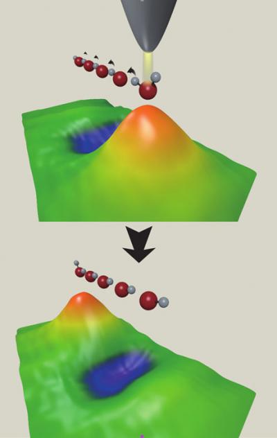
A triple layer of carbon nanotube arrays on a sapphire base is the basis for a new type of terahertz polarizer invented at Rice University. The polarizer could lead to new security and communication devices, sensors and noninvasive medical imaging systems.
Terahertz waves exist at the transition between infrared and microwaves and have unique qualities. They are not harmful and penetrate fabric, wood, plastic and even clouds, but not metal or water. In combination with spectroscopy, they can be used to read what Kono called "spectral fingerprints in the terahertz range"; he said they would, for instance, be useful in a security setting to identify the chemical signatures of specific explosives.

The work by Kono and lead author Lei Ren, who recently earned his doctorate at Rice, makes great use of the basic research into carbon nanotubes for which the university is famous. Co-authors Robert Hauge, a distinguished faculty fellow in chemistry, and his former graduate student Cary Pint developed a way to grow nanotube carpets and to transfer well-aligned arrays of nanotubes from a catalyst to any substrate they chose, limited only by the size of the growth platform.

While Hauge and Pint were developing their nanotube arrays, Kono and his team were thinking about terahertz. Four years ago they came across a semiconducting material, indium antimonide, that would stop or pass terahertz waves, but only in a strong magnetic field and at very low temperatures.

At about the same time, Kono's lab began working with carbon nanotube arrays transferred onto a sapphire substrate by Pint and Hauge. Those aligned arrays -- think of a field of wheat run over by a steamroller -- turned out to be very effective at filtering terahertz waves, as Kono and his team reported in a 2009 paper.

"When the polarization of the terahertz wave was perpendicular to the nanotubes, there was absolutely no attenuation," Kono recalled. "But when the polarization was parallel to the nanotubes, the thickness was not enough to completely kill the transmission, which was still at 30-50 percent."

The answer was clear: Make the polarizer thicker. The current polarizer has three decks of aligned nanotubes on sapphire, enough to effectively absorb all of the incident terahertz radiation. "Our method is unique, and it's simple," he said.

Kono sees use for the device beyond spectroscopy by manipulating it with an electric field, but that will become possible only when all of the nanotubes in an array are of a semiconducting type. As they're made now, batches of nanotubes are a random mix of semiconductors and metallics; recent work by Erik Hároz, a graduate student in Kono's lab, detailed the reasons that nanotubes separated through ultracentrifugation have type-dependent colors. But finding a way to grow specific types of nanotubes is the focus of a great deal of research at Rice and elsewhere.

Co-authors are former Rice postdoctoral researcher Takashi Arikawa and research associate Iwao Kawayama and Professor Masayoshi Tonouchi of the Institute of Laser Engineering at Osaka University, Japan.

The Department of Energy, the National Science Foundation and the Robert A. Welch Foundation supported the research.

Contact: David Ruth david@rice.edu 713-348-6327 Rice University

Friday, January 27, 2012

New type of miniature medical sensor powered by acoustic waves

WEST LAFAYETTE, Ind. – The driving bass rhythm of rap music can be harnessed to power a new type of miniature medical sensor designed to be implanted in the body.

Acoustic waves from music, particularly rap, were found to effectively recharge the pressure sensor. Such a device might ultimately help to treat people stricken with aneurisms or incontinence due to paralysis.

The heart of the sensor is a vibrating cantilever, a thin beam attached at one end like a miniature diving board. Music within a certain range of frequencies, from 200-500 hertz, causes the cantilever to vibrate, generating electricity and storing a charge in a capacitor, said Babak Ziaie, a Purdue University professor of electrical and computer engineering and biomedical engineering.

"The music reaches the correct frequency only at certain times, for example, when there is a strong bass component," he said. "The acoustic energy from the music can pass through body tissue, causing the cantilever to vibrate."

When the frequency falls outside of the proper range, the cantilever stops vibrating, automatically sending the electrical charge to the sensor, which takes a pressure reading and transmits data as radio signals. Because the frequency is continually changing according to the rhythm of a musical composition, the sensor can be induced to repeatedly alternate intervals of storing charge and transmitting data.

New type of miniature medical sensor powered by acoustic waves

This graphic illustrates the principles behind the operation of a new type of miniature medical sensor powered by acoustic waves, including those found in music such as rap, blues, jazz and rock. The device, a pressure sensor, might ultimately help to treat people stricken with aneurisms or incontinence due to paralysis. (Birck Nanotechnology Center, Purdue University)

New type of miniature medical sensor powered by acoustic waves

Researchers have created a new type of miniature pressure sensor, shown here, designed to be implanted in the body. Acoustic waves from music or plain tones drive a vibrating device called a cantilever, generating a charge to power the sensor. (Birck Nanotechnology Center, Purdue University)
"You would only need to do this for a couple of minutes every hour or so to monitor either blood pressure or pressure of urine in the bladder," Ziaie said. "It doesn't take long to do the measurement."

Findings are detailed in a paper to be presented during the IEEE MEMS conference, which will be Jan. 29 to Feb. 2 in Paris. The paper was written by doctoral student Albert Kim, research scientist Teimour Maleki and Ziaie.

"This paper demonstrates the feasibility of the concept," he said.

The device is an example of a microelectromechanical system, or MEMS, and was created in the Birck Nanotechnology Center at the university's Discovery Park. The cantilever beam is made from a ceramic material called lead zirconate titanate, or PZT, which is piezoelectric, meaning it generates electricity when compressed. The sensor is about 2 centimeters long. Researchers tested the device in a water-filled balloon.

A receiver that picks up the data from the sensor could be placed several inches from the patient. Playing tones within a certain frequency range also can be used instead of music.

"But a plain tone is a very annoying sound," Ziaie said. "We thought it would be novel and also more aesthetically pleasing to use music."

Researchers experimented with four types of music: rap, blues, jazz and rock.

"Rap is the best because it contains a lot of low frequency sound, notably the bass," Ziaie said.

The sensor is capable of monitoring pressure in the urinary bladder and in the sack of a blood vessel damaged by an aneurism. Such a technology could be used in a system for treating incontinence in people with paralysis by checking bladder pressure and stimulating the spinal cord to close the sphincter that controls urine flow from the bladder. More immediately, it could be used to diagnose incontinence. The conventional diagnostic method now is to insert a probe with a catheter, which must be in place for several hours while the patient remains at the hospital.

"A wireless implantable device could be inserted and left in place, allowing the patient to go home while the pressure is monitored," Ziaie said.

The new technology offers potential benefits over conventional implantable devices, which either use batteries or receive power through a property called inductance, which uses coils on the device and an external transmitter. Both approaches have downsides. Batteries have to be replaced periodically, and data are difficult to retrieve from devices that use inductance; coils on the implanted device and an external receiver must be lined up precisely, and they can only be about a centimeter apart.

A patent application has been filed for the design.

Writer: Emil Venere, 765-494-4709, venere@purdue.edu Source: Babak Ziaie, 765-494-0725, bziaie@purdue.edu

Wednesday, January 25, 2012

A property of "bilayer graphene" (BLG) that the researchers say is analogous to finding the Higgs boson in particle physics

Bilayer graphene works as an insulator. Research by UC Riverside-led team has potential applications in digital and infrared technologies.

RIVERSIDE, Calif. – A research team led by physicists at the University of California, Riverside has identified a property of "bilayer graphene" (BLG) that the researchers say is analogous to finding the Higgs boson in particle physics.

Graphene, nature's thinnest elastic material, is a one-atom thick sheet of carbon atoms arranged in a hexagonal lattice. Because of graphene's planar and chicken wire-like structure, sheets of it lend themselves well to stacking.

BLG is formed when two graphene sheets are stacked in a special manner. Like graphene, BLG has high current-carrying capacity, also known as high electron conductivity. The high current-carrying capacity results from the extremely high velocities that electrons can acquire in a graphene sheet.

The physicists report online Jan. 22 in Nature Nanotechnology that in investigating BLG's properties they found that when the number of electrons on the BLG sheet is close to 0, the material becomes insulating (that is, it resists flow of electrical current) – a finding that has implications for the use of graphene as an electronic material in the semiconductor and electronics industries.

"BLG becomes insulating because its electrons spontaneously organize themselves when their number is small," said Chun Ning (Jeanie) Lau, an associate professor of physics and astronomy and the lead author of the research paper. "Instead of moving around randomly, the electrons move in an orderly fashion. This is called 'spontaneous symmetry breaking' in physics, and is a very important concept since it is the same principle that 'endows' mass for particles in high energy physics."

Bilayer Graphene Schematic

Caption: The image shows a bilayer graphene schematic. The blue beads represent carbon atoms.

Credit: Lau lab, UC Riverside. Usage Restrictions: None.

Graphene Sheet

Caption: Photo shows a scanning electron microscope image of a graphene sheet (red) suspended between two electrodes. The length of the graphene sheet shown is about 1/100 of the width of a human hair.

Credit: Lau lab, UC Riverside. Usage Restrictions: None.
Lau explained that a typical conductor has a huge number of electrons, which move around randomly, rather like a party with ten thousand guests with no assigned seats at dining tables. If the party only has four guests, however, then the guests will have to interact with each other and sit down at a table. Similarly, when BLG has only a few electrons the interactions cause the electrons to behave in an orderly manner.

New quantum particle

Allan MacDonald, the Sid W. Richardson Foundation Regents Chair in the Department of Physics at The University of Texas at Austin and a coauthor on the research paper, noted that team has measured the mass of a new type of massive quantum particle that can be found only inside BLG crystals.

"The physics which gives these particles their mass is closely analogous to the physics which makes the mass of a proton inside an atomic nucleus very much larger than the mass of the quarks from which it is formed," he said. "Our team's particle is made of electrons, however, not quarks."

MacDonald explained that the experiment the research team conducted was motivated by theoretical work which anticipated that new particles would emerge from the electron sea of a BLG crystal.

"Now that the eagerly anticipated particles have been found, future experiments will help settle an ongoing theoretical debate on their properties," he said.

Practical applications

An important finding of the research team is that the intrinsic "energy gap" in BLG grows with increasing magnetic field.

In solid state physics, an energy gap (or band gap) refers to an energy range in a solid where no electron states can exist. Generally, the size of the energy gap of a material determines whether it is a metal (no gap), semiconductor (small gap) or insulator (large gap). The presence of an energy gap in silicon is critical to the semiconductor industry since, for digital applications, engineers need to turn the device 'on' or conductive, and 'off' or insulating.

Single layer graphene (SLG) is gapless, however, and cannot be completely turned off because regardless of the number of electrons on SLG, it always remains metallic and a conductor.

"This is terribly disadvantageous from an electronics point of view," said Lau, a member of UC Riverside's Center for Nanoscale Science and Engineering. "BLG, on the other hand, can in fact be turned off. Our research is in the initial phase, and, presently, the band gap is still too small for practical applications. What is tremendously exciting though is that this work suggests a promising route – trilayer graphene and tetralayer graphene, which are likely to have much larger energy gaps that can be used for digital and infrared technologies. We already have begun working with these materials."

###

Lau and MacDonald were joined in the research by J. Velasco Jr. (the first author of the research paper), L. Jing, W. Bao, Y. Lee, P. Kratz, V. Aji, M. Bockrath, and C. Varma at UCR; R. Stillwell and D. Smirnov at the National High Magnetic Field Laboratory, Tallahassee, Fla.; and Fan Zhang and J. Jung at The University of Texas at Austin.

The research was supported by grants from the National Science Foundation, Office of Naval Research, FENA Focus Center, and other agencies.

The University of California, Riverside (www.ucr.edu) is a doctoral research university, a living laboratory for groundbreaking exploration of issues critical to Inland Southern California, the state and communities around the world. Reflecting California's diverse culture, UCR's enrollment has exceeded 20,500 students. The campus will open a medical school in 2013 and has reached the heart of the Coachella Valley by way of the UCR Palm Desert Center. The campus has an annual statewide economic impact of more than $1 billion.

A broadcast studio with fiber cable to the AT&T Hollywood hub is available for live or taped interviews. UCR also has ISDN for radio interviews. To learn more, call 951-UCR-NEWS.

Contact: Iqbal Pittalwala iqbal@ucr.edu 951-827-6050 University of California - Riverside

Monday, January 23, 2012

Invisible to Water, thinness of Graphene Enables Near Perfect Wetting Transparency

Nature Materials Study: Graphene “Invisible” to Water. Engineers at Rensselaer Polytechnic Institute and Rice University Discover How the Extreme Thinness of Graphene Enables Near-Perfect Wetting Transparency.

Graphene is the thinnest material known to science. The nanomaterial is so thin, in fact, water often doesn’t even know it’s there.

Engineering researchers at Rensselaer Polytechnic Institute and Rice University coated pieces of gold, copper, and silicon with a single layer of graphene, and then placed a drop of water on the coated surfaces. Surprisingly, the layer of graphene proved to have virtually no impact on the manner in which water spreads on the surfaces.

Results of the study were published Sunday in the journal Nature Materials. The findings could help inform a new generation of graphene-based flexible electronic devices. Additionally, the research suggests a new type of heat pipe that uses graphene-coated copper to cool computer chips.

The discovery stemmed from a cross-university collaboration led by Rensselaer Professor Nikhil Koratkar and Rice Professor Pulickel Ajayan.

“We coated several different surfaces with graphene, and then put a drop of water on them to see what would happen. What we saw was a big surprise—nothing changed. The graphene was completely transparent to the water,” said Koratkar, a faculty member in the Department of Mechanical, Aerospace, and Nuclear Engineering and the Department of Materials Science and Engineering at Rensselaer. “The single layer of graphene was so thin that it did not significantly disrupt the non-bonding van der Waals forces that control the interaction of water with the solid surface. It’s an exciting discovery, and is another example of the unique and extraordinary characteristics of graphene.”

Invisible to Water, thinness of Graphene Enables Near Perfect Wetting TransparencyEssentially an isolated layer of the graphite found commonly in our pencils or the charcoal we burn on our barbeques, graphene is single layer of carbon atoms arranged like a nanoscale chicken-wire fence. Graphene is known to have excellent mechanical properties. The material is strong and tough and because of its flexibility can evenly coat nearly any surface. Many researchers and technology leaders see graphene as an enabling material that could greatly advance the advent of flexible, paper-thin devices and displays. Used as a coating for such devices, the graphene would certainly come into contact with moisture. Understanding how graphene interacts with moisture was the impetus behind this new study.

The spreading of water on a solid surface is called wetting. Calculating wettability involves placing a drop of water on a surface, and then measuring the angle at which the droplet meets the surface. The droplet will ball up and have a high contact angle on a hydrophobic surface. Inversely, the droplet will spread out and have a low contact angle on a hydrophilic surface.

The contact angle of gold is about 77 degrees. Koratkar and Ajayan found that after coating a gold surface with a single layer of graphene, the contact angle became about 78 degrees. Similarly, the contact angle of silicon rose from roughly 32 degrees to roughly 33 degrees, and copper increased from around 85 degrees to around 86 degrees, after adding a layer of graphene.

These results surprised the researchers. Graphene is impermeable, as the tiny spaces between its linked carbon atoms are too small for water,or a single proton, or anything else to fit through. Because of this, one would expect that water would not act as if it were on gold, silicon, or copper, since the graphene coating prevents the water from directly contacting these surfaces. But the research findings clearly show how the water is able to sense the presence of the underlying surface, and spreads on those surfaces as if the graphene were not present at all.

As the researchers increased the number of layers of graphene, however, it became less transparent to the water and the contact angles jumped significantly. After adding six layers of graphene, the water no longer saw the gold, copper, or silicon and instead behaved as if it was sitting on graphite.

The reason for this perplexing behavior is subtle. Water forms chemical or hydrogen bonds with certain surfaces, while the attraction of water to other surfaces is dictated by non-bonding interactions called van der Waals forces. These non-bonding forces are not unlike a nanoscale version of gravity, Koratkar said. Similar to how gravity dictates the interaction between the Earth and sun, van der Waals forces dictate the interaction between atoms and molecules.

In the case of gold, copper, silicon, and other materials, the van der Waals forces between the surface and water droplet determine the attraction of water to the surface and dictate how water spreads on the solid surface. In general, these forces have a range of at least several nanometers. Because of the long range, these forces are not disrupted by the presence of a single-atom-thick layer of graphene between the surface and the water. In other words, the van der Waals forces are able to “look through” ultra-thin graphene coatings, Koratkar said.

If you continue to add additional layers of graphene, however, the van der Waals forces increasingly “see” the carbon coating on top of the material instead of the underlying surface material. After stacking six layers of graphene, the separation between the graphene and the surface is sufficiently large to ensure that the van der Waals forces can now no longer sense the presence of the underlying surface and instead only see the graphene coating. On surfaces where water forms hydrogen bonds with the surface, the wetting transparency effect described above does not hold because such chemical bonds cannot form through the graphene layer.

Along with conducting physical experiments, the researchers verified their findings with molecular dynamics modeling as well as classical theoretical modeling.

“We found that van der Waals forces are not disrupted by graphene. This effect is an artifact of the extreme thinness of graphene—which is only about 0.3 nanometers thick,” Koratkar said. “Nothing can rival the thinness of graphene. Because of this, graphene is the ideal material for wetting angle transparency.”

“Moreover, graphene is strong and flexible, and it does not easily crack or break apart,” he said. “Additionally, it is easy to coat a surface with graphene using chemical vapor deposition, and it is relatively uncomplicated to deposit uniform and homogeneous graphene coatings over large areas. Finally, graphene is chemically inert, which means a graphene coating will not oxidize away. No single material system can provide all of the above attributes that graphene is able to offer.”

A practical application of this new discovery is to coat copper surfaces used in dehumidifiers. Because of its exposure to water, copper in dehumidifier systems oxidizes, which in turn decreases its ability to transfer heat and makes the entire device less efficient. Coating the copper with graphene prevents oxidation, the researchers said, and the operation of the device is unaffected because graphene does not change the way water interacts with copper. This same concept may be applied to improve the ability of heat pipes to dissipate heat from computer chips, Koratkar said.

“It’s an interesting idea. The graphene doesn’t cause any significant change to the wettability of copper, and at the same time it passivates the copper surface and prevents it from oxidizing,” he said.

Along with Koratkar and Ajayan, co-authors of the paper are Yunfeng Shi, assistant professor in the Department of Materials Science and Engineering at Rensselaer; Rensselaer mechanical engineering graduate students Javad Rafiee, Abhay Thomas, and Fazel Yavari; Rensselaer physics graduate student Xi Mi; and Rice mechanical and materials engineering graduate student Hemtej Gullapalli.

This research was supported in part by the Advanced Energy Consortium (AEC); the National Science Foundation (NSF); and the Office of Naval Research (ONR) graphene Multidisciplinary University Research Initiative (MURI).

Results of the study are detailed in the Nature Materials paper “Wetting transparency of graphene.” See the paper online at: Wetting transparency of graphene

Contact: Michael Mullaney: mullam@rpi.edu 518-276-6161 Rensselaer Polytechnic Institute

Saturday, January 21, 2012

Tweaking small parts dramatically increases amount of sunlight solar cells convert into electricity

In Solar Cells, Tweaking the Tiniest of Parts Yields Big Jump in Efficiency.

Company led by university researchers employs charged quantum dots to increase the efficiency of solar cell technology

Summary: -- Researchers from the University at Buffalo, Army Research Laboratory and Air Force Office of Scientific Research have developed a new, nanomaterials-based technology that has the potential to increase the efficiency of photovoltaic cells up to 45 percent.

-- Specifically, the researchers have shown that embedding charged quantum dots into solar cells can improve electrical output by enabling the cells to harvest infrared light, and by increasing the lifetime of photoelectrons. The technology can be applied to many different photovoltaic structures.

-- A new company the researchers founded, OPtoElectronic Nanodevices LLC. (OPEN LLC), is commercializing this technology.

BUFFALO, N.Y. -- By tweaking the smallest of parts, a trio of University at Buffalo engineers is hoping to dramatically increase the amount of sunlight that solar cells convert into electricity.

With military colleagues, the UB researchers have shown that embedding charged quantum dots into photovoltaic cells can improve electrical output by enabling the cells to harvest infrared light, and by increasing the lifetime of photoelectrons.

Vladimir Miti

Electrical engineer Vladimir Mitin and colleagues have significantly increased the electrical output of solar cells by embedding charged quantum dots in them.
The research appeared online last May in the journal Nano Letters. The research team included Vladimir Mitin, Andrei Sergeev and Nizami Vagidov, faculty members in UB's electrical engineering department; Kitt Reinhardt of the Air Force Office of Scientific Research; and John Little and advanced nanofabrication expert Kimberly Sablon of the U.S. Army Research Laboratory.

Mitin, Sergeev and Vagidov have founded a company, OPtoElectronic Nanodevices LLC. (OPEN LLC.), to bring the innovation to the market.

The idea of embedding quantum dots into solar panels is not new: According to Mitin, scientists had proposed about a decade ago that this technique could improve efficiency by allowing panels to harvest invisible, infrared light in addition to visible light. However, intensive efforts in this direction have previously met with limited success.

The UB researchers and their colleagues have not only successfully used embedded quantum dots to harvest infrared light; they have taken the technology a step further, employing selective doping so that quantum dots within the solar cell have a significant built-in charge.

This built-in charge is beneficial because it repels electrons, forcing them to travel around the quantum dots. Otherwise, the quantum dots create a channel of recombination for electrons, in essence "capturing" moving electrons and preventing them from contributing to electric current.

The technology has the potential to increase the efficiency of solar cells up to 45 percent, said Mitin, a SUNY Distinguished Professor. Through UB's Office of Science, Technology Transfer and Economic Outreach (STOR), he and his colleagues have filed provisional patent applications to protect their technology.

"Clean technology will really benefit the region, the state, the country," Mitin said. "With high-efficiency solar cells, consumers can save money and providers can have a smaller solar field that produces more energy."

Mitin and his colleagues have already invested significant amounts of time in developing the quantum dots with a built-in-charge, dubbed "Q-BICs." To further enhance the technology and bring it to the market, OPEN LLC is now seeking funding from private investors and federal programs.

The University at Buffalo is a premier research-intensive public university, a flagship institution in the State University of New York system and its largest and most comprehensive campus. UB's more than 28,000 students pursue their academic interests through more than 300 undergraduate, graduate and professional degree programs. Founded in 1846, the University at Buffalo is a member of the Association of American Universities.

Contact: Charlotte Hsu chsu22@buffalo.edu 716-645-4655 University at Buffalo

Thursday, January 19, 2012

Disease fighting protein in our teardrops destroys dangerous bacteria

Novel technology that reveals lysozymes have jaws could aid in early cancer diagnosis — Irvine, Calif., January 19, 2012 —

A disease-fighting protein in our teardrops has been tethered to a tiny transistor, enabling UC Irvine scientists to discover exactly how it destroys dangerous bacteria. The research could prove critical to long-term work aimed at diagnosing cancers and other illnesses in their very early stages.

Ever since Nobel laureate Alexander Fleming found that human tears contain antiseptic proteins called lysozymes about a century ago, scientists have tried to solve the mystery of how they could relentlessly wipe out far larger bacteria. It turns out that lysozymes have jaws that latch on and chomp through rows of cell walls like someone hungrily devouring an ear of corn, according to findings that will be published Jan. 20 in the journal Science.

“Those jaws chew apart the walls of the bacteria that are trying to get into your eyes and infect them,” said molecular biologist and chemistry professor Gregory Weiss, who co-led the project with associate professor of physics & astronomy Philip Collins.

The researchers decoded the protein’s behavior by building one of the world’s smallest transistors – 25 times smaller than similar circuitry in laptop computers or smartphones. Individual lysozymes were glued to the live wire, and their eating activities were monitored.

“Our circuits are molecule-sized microphones,” Collins said. “It’s just like a stethoscope listening to your heart, except we’re listening to a single molecule of protein.”

Gregory Weiss

Gregory Weiss
It took years for the UCI scientists to assemble the transistor and attach single-molecule teardrop proteins. The scientists hope the same novel technology can be used to detect cancerous molecules. It could take a decade to figure out but would be well worth it, said Weiss, who lost his father to lung cancer.

“If we can detect single molecules associated with cancer, then that means we’d be able to detect it very, very early,” Weiss said. “That would be very exciting, because we know that if we treat cancer early, it will be much more successful, patients will be cured much faster, and costs will be much less.”

The project was sponsored by the National Cancer Institute and the National Science Foundation. Co-authors of the Science paper are Yongki Choi, Issa Moody, Patrick Sims, Steven Hunt, Brad Corso and Israel Perez.

About the University of California, Irvine: Founded in 1965, UCI is a top-ranked university dedicated to research, scholarship and community service. Led by Chancellor Michael Drake since 2005, UCI is among the most dynamic campuses in the University of California system, with nearly 28,000 undergraduate and graduate students, 1,100 faculty and 9,000 staff. Orange County’s second-largest employer, UCI contributes an annual economic impact of $4 billion. For more UCI news, visit www.today.uci.edu

News Radio: UCI maintains on campus an ISDN line for conducting interviews with its faculty and experts. Use of this line is available for a fee to radio news programs/stations that wish to interview UCI faculty and experts. Use of the ISDN line is subject to availability and approval by the university. +sookie tex

University of California, Irvine - Irvine, CA 92697 : 949-824-5011. Media Contact: Janet Wilson University Communications 949-824-3969 janethw@uci.edu

Tuesday, January 17, 2012

Microtweezers to assemble structures in microelectromechanical systems 'MEMS'

WEST LAFAYETTE, Ind. - Researchers have created new "microtweezers" capable of manipulating objects to build tiny structures, print coatings to make advanced sensors, and grab and position live stem cell spheres for research.

The microtweezers might be used to assemble structures in microelectromechanical systems, or MEMS, which contain tiny moving parts. MEMS accelerometers and gyroscopes currently are being used in commercial products. A wider variety of MEMS devices, however, could be produced through a manufacturing technology that assembles components like microscopic Lego pieces moved individually into place with microtweezers, said Cagri Savran (pronounced Chary Savran), an associate professor of mechanical engineering at Purdue University.

"We've shown how this might be accomplished easily, using new compact and user-friendly microtweezers to assemble polystyrene spheres into three-dimensional shapes," he said.

Research findings were detailed in a paper that appeared online in December in the Journal of Microelectromechanical Systems, or JMEMS. The paper was written by Savran, mechanical engineering graduate students Bin-Da Chan and Farrukh Mateen, electrical and computer engineering graduate student Chun-Li Chang, and biomedical engineering doctoral student Kutay Icoz.

The new tool contains three main parts: a thimble knob from a standard micrometer, a two-pronged tweezer made from silicon, and a "graphite interface," which converts the turning motion of the thimble knob into a pulling-and-pushing action to open and close the tweezer prongs. No electrical power sources are needed, increasing the potential for practical applications. Other types of microtweezers have been developed and are being used in research. However, the new design is simpler both to manufacture and operate, Savran said.

a new type of microtweezers

Purdue researchers have created a new type of microtweezers capable of manipulating objects to build tiny structures, print coatings to make advanced sensors, and grab and position live stem cell spheres for research. (Birck Nanotechnology Center photo)

a new type of microtweezers

The new microtweezers might be used to assemble structures in microelectromechanical systems, or MEMS, which contain tiny moving parts. The researchers have shown how the device can be used to assemble tiny polystyrene spheres, each with a diameter of 40 micrometers, at left, into three-dimensional shapes. The device also might be used to weigh tiny particles by placing them onto the tip of a structure called a microcantilever, at right. (Birck Nanotechnology Center photo)
The design contains a one-piece "compliant structure," which is springy like a bobby pin or a paperclip. Most other microtweezers require features such as hinges or components that move through heat, magnetism or electricity, complex designs that are expensive to manufacture and relatively difficult to operate in various media, he said.

The tweezers make it feasible to precisely isolate individual stem cell spheres from culture media and to position them elsewhere. Currently, these spheres are analyzed in large groups, but microtweezers could provide an easy way to study them by individually selecting and placing them onto analytical devices and sensors.

"We currently are working to weigh single micro particles, individually selected among many others, which is important because precise measurements of an object's mass reveal key traits, making it possible to identify composition and other characteristics," Savran said. "This will now be as easy as selecting and weighing a single melon out of many melons in a supermarket."

That work is a collaboration with the research group of Timothy Ratliff, the Robert Wallace Miller Director of Purdue's Center for Cancer Research.

The microtweezers also could facilitate the precision printing of chemical or protein dots onto "microcantilevers," strips of silicon that resemble tiny diving boards. The microcantilevers can be "functionalized," or coated with certain chemicals or proteins that attract specific molecules and materials. Because they vibrate at different frequencies depending on what sticks to the surface, they are used to detect chemicals in the air and water.

Generally, microcantilevers are functionalized to detect one type of substance by exposing them to fluids, Savran said. However, being able to microprint a sequence of precisely placed dots of different chemicals on each cantilever could make it possible to functionalize a device to detect several substances at once. Such a sensing technology also would require a smaller sample size than conventional diagnostic technologies, making it especially practical.

The new microtweezers are designed to be attached easily to "translation stages" currently used in research. These stages are essentially platforms on which to mount specimens for viewing and manipulating. Unlike most other microtweezers, the new device is highly compact and portable and can be easily detached from a platform and brought to another lab while still holding a micro-size object for study, Savran said.

The two-pronged tweezer is micromachined in a laboratory called a "clean room" with the same techniques used to create microcircuits and computer chips. The research was based at the Birck Nanotechnology Center in Purdue's Discovery Park.
Purdue has filed for a provisional patent on the design.

Writer: Emil Venere, 765-494-4709, venere@purdue.edu, Source: Cagri A. Savran, 765 494-8601, savran@purdue.edu

Saturday, January 14, 2012

Paul Alivisatos director Berkeley Lab wins Wolf Prize in Chemistry with fellow nanoscience expert Charles Lieber

Paul Alivisatos director Berkeley Lab wins Wolf Prize in Chemistry with fellow nanoscience expert Charles Lieber.

Paul Alivisatos, director of the U.S. Department of Energy (DOE)'s Lawrence Berkeley National Laboratory (Berkeley Lab) and the University of California (UC) Berkeley's Larry and Diane Bock Professor of Nanotechnology, has won the prestigious Wolf Foundation Prize in Chemistry for 2012. Alivisatos is an internationally recognized authority on nanochemistry and a pioneer in the synthesis of semiconductor quantum dots and multi-shaped artificial nanostructures. He shares this year's Wolf Prize in Chemistry with fellow nanoscience expert Charles Lieber of Harvard University. The Wolf Foundation, which is based in Israel, has been recognizing outstanding scientists and artists annually since 1978. This year's winners include the renowned tenor and conductor Placido Domingo.

"I am greatly honored to share the 2012 Wolf Prize in Chemistry with my friend Charlie Lieber from Harvard," said Alivisatos. "It is also thrilling to be in the same class of Wolf Prize recipients as Placido Domingo."

The Wolf Foundation Prize, which is awarded in the scientific fields of agriculture, chemistry, mathematics, medicine and physics, and in a variety of the arts, consists of a certificate and a monetary award of $100,000. Recipients are selected by an international committee of recognized experts in each field. As of 2011, a total of 253 scientists and artists from 23 countries have been honored, including four scientists from Berkeley Lab – Gabor Somorjai, Peter Schultz, Alexander Pines and George Pimentel. Laureates receive their awards from the President of Israel at a special ceremony of Israel´s Parliament in Jerusalem.


Berkeley Lab director Paul Alivisatos

Caption: This is Berkeley Lab director Paul Alivisatos. Credit: Roy Kaltschmidt, Berkeley Lab, Usage Restrictions: None.
The citation on Alivisatos' chemistry prize credits him for his development of the colloidal inorganic nanocrystal as a building block of nanoscience and for "making fundamental contributions to controlling the synthesis of these particles, to measuring and understanding their physical properties, and to utilizing their unique properties for applications ranging from light generation and harvesting to biological imaging."

Alivistos is widely recognized as the man who demonstrated that semiconductor nanocrystals can be grown into two-dimensional rods and other shapes as opposed to spheres. This achievement paved the way for a slew of new applications including biomedical diagnostics, revolutionary photovoltaic cells and LED materials. He also demonstrated key applications of nanocrystals in biological imaging and renewable energy. Prior to his research, all non-metal nanocrystals were dot-shaped, meaning they were essentially one-dimensional.

U.S. Energy Secretary and Nobel laureate Steven Chu once said of Alivisatos, "He has been a world leader in the synthesis of artificial nanostructures and quantum dot technology, and one of the principal scientific drivers behind the use of nanoscience technologies to create a new generation of solar photovoltaic cells."

Alivisatos was born in Chicago on November 12, 1959. He lived there until the age of 10, when his family moved to Athens, Greece, where he would remain through high school. Alivisatos has said of his years in Greece that it was a great experience for him because he had to learn the Greek language and culture then catch up with the more advanced students.

"When I found something very interesting it was sometimes a struggle for me to understand it the very best that I could," he has said of that experience. "That need to work harder became an important motivator for me."

Alivisatos returned to the United States to attend the University of Chicago where in 1981 he earned his B.A. in Chemistry with honors. He attended graduate school at UC Berkeley, graduating with a Ph.D. in Chemical Physics in 1986. He went to AT&T Bell Labs as a post-doctoral fellow and returned to Berkeley in 1988 as an assistant professor of chemistry. He was promoted to associate professor in 1993 and full professor in 1995. He served as UC Berkeley's Chancellor's Professor from 1998 to 2001, and added an appointment as a professor of materials science and engineering in 1999.

Alivisatos' affiliation with Berkeley Lab began in 1991 when he joined the staff of the Materials Sciences Division. He rose to become director of that division in 2002, a position he held for six years. In 2001 he was named to head a new U.S. Department of Energy center for nanoscience called the Molecular Foundry, which is hosted at Berkeley Lab. He continued to direct research at the Foundry until 2005. From 2005 to 2007 he served as Berkeley Lab's Associate Laboratory Director for Physical Science.

Alivisatos was appointed to lead Berkeley Lab's Materials Sciences Division by then Lab director Charles Shank who hailed him as "one of the fathers of nanoscience." Among the first to publish scientific results in the field, Alivisatos went on to publish well over 100 papers.

The many awards and recognitions Alivisatos has received for his science include the Ernest Orlando Lawrence Award, the Eni Italgas Prize for Energy and Environment, the Rank Prize for Optoelectronics Award, the Wilson Prize, the Coblentz Award for Advances in Molecular Spectroscopy, and the U.S. Department of Energy's Award for Sustained Outstanding Research in Materials Chemistry and Outstanding Scientific Accomplishment in Materials Chemistry. In addition, Alivisatos has held fellowships with the American Association for the Advancement of Science, the American Physical Society, the American Chemical Society and the Alfred P. Sloan Foundation. He is a member of the National Academy of Sciences and the American Academy of Arts and Sciences.

### +sookie tex

Lawrence Berkeley National Laboratory addresses the world's most urgent scientific challenges by advancing sustainable energy, protecting human health, creating new materials, and revealing the origin and fate of the universe. Founded in 1931, Berkeley Lab's scientific expertise has been recognized with 13 Nobel prizes. The University of California manages Berkeley Lab for the U.S. Department of Energy's Office of Science. For more visit www.lbl.gov.

Contact: Lynn Yarris lcyarris@lbl.gov 510-486-5375 DOE/Lawrence Berkeley National Laboratory

Friday, January 13, 2012

Heat shock protein 90's mechano-chemical cycle is dominated by thermal fluctuations

Energy-saving chaperon Hsp90 Large conformational changes without ATP consummation.

A special group of proteins, the so-called chaperons, helps other proteins to obtain their correct conformation. Until now scientists supposed that hydrolyzing ATP provides the energy for the large conformational changes of chaperon Hsp90. Now a research team from the Nanosystems Initiative Munich could prove that Hsp90 utilizes thermal fluctuations as the driving force for its conformational changes. The renowned journal PNAS reports on their findings.

ATP is the major energy source for most organisms and ATPases are the machines, which utilize this fuel, for example to move muscles or cargo in our body. The very abundant chaperone protein Hsp90 has such an ATPase in each of its two monomers. During the last years experiments had suggested that the movement and conformational changes of ATPase proteins are in general strictly linked to ATP binding and hydrolysis (i.e. fuel consumption).

To probe this theory Thorsten Hugel, Professor at the Technische Universitaet Muenchen (TUM) and member of the Nanosystems Initiative Munich (NIM), and his team designed a special three color single-molecule FRET (Förster resonance energy transfer) assay with alternating laser excitation (ALEX) for simultaneous observation of ATP binding and conformational changes. Unexpectedly the experiments revealed that binding and hydrolysis of ATP is not correlated with the large conformational changes of Hsp90. Hsp90 is instead a highly flexible machinery driven by thermal fluctuations.

3-Color Single-Molecule FRET Setup

Caption: With their specially designed three-color single-molecule FRET (Foerster resonance energy transfer) assay with alternating laser excitation (ALEX) for simultaneous observation of ATP binding and conformational changes professor Hugel and his team could prov, that Hsp90 utilizes thermal fluctuations for its large conformational changes. Credit: Christoph Ratzke. Usage Restrictions: None.
"Thermal fluctuations are random changes in the structure of the protein – they can be thought of as collisions with water molecules in the environment, which move rather violently at the temperatures in a living organism," says Thorsten Hugel. "Using these clashes to switch back and forth between different conformations, saves Hsp90 valuable ATP." But then what is the task of ATPase in the Hsp90 chaperone? The scientists suspect that co-chaperones and substrate proteins alter the system so that ATP binding or hydrolysis can take a crucial task.

With the newly developed experimental setup, it is now possible to investigate the very complex system in greater detail to resolve this important question. The Munich biophysicists therewith offer a new perspective on the energy conversion in molecular machines.

###

The work was supported by grants from the DFG (Hu997/9-1, SFB 863) and the Cluster of Excellence Nanosystems Initiative Munich (NIM) and the NanoBio-Technology program of the Elite Network of Bavaria.

Original publication:

Heat shock protein 90's mechano-chemical cycle is dominated by thermal fluctuations Christoph Ratzke, Felix Berkemeier, and Thorsten Hugel, PNAS, January 3, 2012 vol. 109, no. 1, 161-166 – Doi: 10.1073/pnas.1107930108

Contact: Dr. Andreas Battenberg battenberg@zv.tum.de 49-892-891-0510 Technische Universitaet Muenchen

Wednesday, January 11, 2012

Broad scientific approach to studying rare earth materials needed to ensure continued deployment of clean energy technologies

Broad scientific approach to studying rare earth materials needed to ensure continued deployment of clean energy technologies.

A few short decades ago, few could have imagined that the world would be seriously concerned over something called dysprosium. Also known as number 66 on the periodic table, dysprosium was once just another element for chemistry students to memorize but is now one of the most sought-after and critically needed materials on the planet.

Belonging to a family of elements known as lanthanides—also called rare earths—dysprosium and other rare earths are used in almost every high-tech gadget and clean energy technology invented in the last 30 years, from smart phones to wind turbines to hybrid cars. Although the United States was self-sufficient in rare earths or obtained them on the free market until the early 2000s, the vast majority are now mined in China and the supply has been subject to fluctuations. The Department of Energy’s (DOE) Lawrence Berkeley National Laboratory (Berkeley Lab) aims to change the status quo by reviving the study of these critical materials to better understand how to extract them, use them more efficiently, reuse and recycle them and find substitutes for them.

In its 2011 Critical Material Strategy released last month, the DOE said that “supply challenges for five rare earth metals (dysprosium, neodymium, terbium, europium and yttrium) may affect clean energy technology deployment in the years ahead.” It also recommended enhanced training of scientists and engineers to “address vulnerabilities and realize opportunities related to critical materials.”

rare earths

The top matrix shows the supply risk and importance to clean energy of certain elements in the short term (present-2015). The bottom matrix shows the medium term (2015-2025). (Source: DOE)
“If we are going to achieve what we need to do in terms of managing climate change, we absolutely have to fix the materials problem—it’s the linchpin for clean energy technologies,” said Frances Houle, a Berkeley Lab scientist who is Director of Strategic Initiatives in the Chemical Sciences Division. “Because Berkeley Lab is such a broad institution, many of the pieces required are already here. We have the chemistry, the earth science, the materials science, the theory. Not very many institutions can say that.”

Like coal and gold, the rare earths are mined out of the ground. However, in any given ore, they are mixed together with other rare earths. So although they are not actually rare, they are difficult to mine. “They’re in low concentration, and it’s very hard to mine them and separate them out, so it’s challenging and extremely energy-intensive to produce rare earth materials ready for industrial manufacturers; it requires a lot of electricity, water and chemicals,” said Berkeley Lab Senior Scientist David Shuh. “This area of study has been ignored over the last two decades, largely due to insufficient research and development support.”

Shuh is the lead investigator on a Berkeley Lab project that takes a multidisciplinary approach to the issues, reinvigorating the study of the fundamental chemistry and materials sciences while taking advantage of advances in nanoscience, earth sciences, genomics and energy analysis techniques to devise innovative solutions.

While the United States has some scientists working in the rare earth field, China has at least 100 times as many. “The U.S. used to have the leadership in the chemistry and materials sciences of these materials, but now we are losing competitive advantages in these areas,” Shuh said. “We need to rev up rare earth science from top to bottom if we want to retain leadership in the use of these critical materials.”

Batteries, photovoltaics and lighting are just a few of the industries that could be crippled without reliable access to materials such as cerium, neodymium and terbium. Dysprosium is used in high-performance magnets (for cars, wind turbines, disc drives and a myriad of other uses) essential for the implementation of many clean energy technologies. In addition to the rare earths, there are a number of other so-called “energy critical elements” in other parts of the periodic table, including lithium, helium, cobalt and rhenium, that are crucial to a clean energy economy and are currently found in a limited number of places.


The resources devoted to studying the rare earths have not changed much since around the time the color television was invented. But in the meantime, their price has skyrocketed, increasing by nearly a factor of 1,000 in some cases, and scientists and engineers continue to rely on decades old science to address the energy challenge today. Moreover, new ways to use rare earths are being developed all the time.

More advanced study of the chemical and materials properties of the energy critical elements would not only aid in mining, separating, processing, and using them in current applications more efficiently but would also allow scientists to better understand—and thus find—substitutes for them. Plus, it should accelerate technological breakthroughs. “With better science, you’ll have better discovery and better technology,” Houle said. “It’s not feasible to go on a fishing expedition any more. You must have theory to guide the discovery effort.”

The Chemical Sciences Division of Berkeley Lab is world renowned in the study of actinides, a close neighbor of the lanthanides (rare earths) and which bear some chemical similarities. One goal of Shuh’s project is to improve understanding of their fundamental interactions by coupling theory to spectroscopic results, paving the way for the design of more efficient element-specific separations and development of new applications in fields such as lighting and biotechnology.

Complementing this approach, Berkeley Lab’s Materials Science Division will focus on basic research into understanding the properties of materials to come up with new alternatives that mimic those properties. “For example, certain wind turbines and motors rely on neodymium magnets. A better microscopic understanding may point toward new replacement materials containing elements that are more environmentally friendly or abundant,” said Jeff Neaton, deputy director of the division. “It may be that replacements draw on a combination of materials, a composite or assembly, or reduced dimensionality, as in nanostructures.”

Neaton added that recent advances in nanoscience, which allows researchers to synthesize and control materials at the level of atoms and molecules and a few tens of nanometers, has potential to play a large role in the process. Also, new nanoscale characterization tools and theory could bring breakthroughs in understanding that will be important in guiding the search for replacement materials.

Berkeley Lab’s Earth Sciences Division has deep experience in the modeling of subsurface chemical processes and in geochemical analysis of mineral surface structure and pore chemistry, expertise that will be useful in studying new ways to recover rare earth elements. Another approach would take advantage of “-omics” methods (which includes genomics and proteomics) to identify microorganisms that could aid in releasing rare earths from minerals.

At the other end of the process but encompassing the overall use of rare earth materials, researchers Jim McMahon and Eric Masanet of Berkeley Lab’s Environmental Energy Technologies Division specialize in analyzing industrial processes and quantifying the environmental and energy implications. Their lifecycle analysis of critical materials will focus on how to reuse and recycle them in efficient and environmentally acceptable ways.

Currently, the rare earth elements in computers, smart phones and other electronic gadgets are often either thrown away or sent abroad to be recovered—typically using low-cost labor and environmentally hazardous means. Today’s cell phones use 40 different elements; a Toyota Prius contains approximately 30 pounds of rare earth material.

“The materials are not designed to be easily recovered from the product, so we would look at the entire process of how something is manufactured, such as car batteries, and see if the battery can be designed and manufactured in a way to get the same performance but so that not only do we not waste anything but also puts the metal in a form that we can get it back,” said McMahon.

The analysis and modeling adds two other dimensions missing from many other lifecycle analyses: place and time. “If you look at a plant in California versus Wyoming, there’s different weather, different water availability, different pollutants, so it matters where you are,” McMahon said. “It also matters when you do it: things like photovoltaics are evolving, so five years from now, it will be different materials and different technologies.”

Many factors ranging from political events to environmental trends to changes in markets for products influence the availability of resources for manufactured goods. “A critical material today wasn’t a critical material 20 or 30 years ago,” Houle said. “Who knows what the crisis is going to be in 30 years. The main goal should be to be more resilient to shortages. Having alternatives and good reuse and recycling programs is essential.”

# # #

Lawrence Berkeley National Laboratory addresses the world’s most urgent scientific challenges by advancing sustainable energy, protecting human health, creating new materials, and revealing the origin and fate of the universe. Founded in 1931, Berkeley Lab’s scientific expertise has been recognized with 13 Nobel prizes. The University of California manages Berkeley Lab for the U.S. Department of Energy’s Office of Science. For more, visit www.lbl.gov.

Julie Chao (510)486-6491 JHChao@lbl.gov

Tuesday, January 10, 2012

“repair-and-go” method: A flexible microcapsule filled with a solution of nanoparticles would be applied to a damaged surface

PITTSBURGH—Like the human body, a digital device often suffers a few bruises and scratches within a lifetime. As in medicine, these injuries can be easily detected and repaired (or healed). At other times, however, a digital device may sustain hard-to-pinpoint nanoscale scratches, which can cause the device as a whole to malfunction.

In a paper published today, Jan. 10, in Nature Nanotechnology, a team of researchers from the University of Pittsburgh and the University of Massachusetts Amherst (UMass) propose a “repair-and-go” approach to fixing malfunctions caused by small-surface cracks on any digital device or part before it hits store shelves.

“Anything that’s a machine with a surface is affected by these small-scale cracks,” said Anna Balazs, Distinguished Professor of Chemical and Petroleum Engineering in Pitt’s Swanson School of Engineering and coinvestigator on the project. “These are surfaces that play a role in almost anything, especially functionality.”

The Pitt-UMass research team approach was inspired by the ability of white blood cells in the body to heal wounds on-site. Balazs and Pitt colleagues first came up with a theoretical “repair-and-go” method: A flexible microcapsule filled with a solution of nanoparticles would be applied to a damaged surface; it would then repair defects by releasing nanoparticles into them. Using nanoparticles and droplets of oil stabilized with a polymer surfactant—compounds that lower the surface tension of a liquid—the UMass team actualized the theory, showing that these microcapsules found the cracks and delivered the nanoparticle contents into them. Balazs proposes that manufacturers use this method as a last step in the building process.

Anna Balazs

Anna Balazs
“The repair-and-go method can extend the lifetime of any system or device,” she said. “Additionally, it could be used as a repair method after a crack has been found.”

Original research by Balazs and her team was published in ACS Nano and then reported on in Nature Nanotechnology’s “News and Views” section in September 2010. To read more about the healing process of devices, visit www.nature.com/nnano/journal/.

Contact: B. Rose Huber rhuber@pealcenter.org 412-624-4356 University of Pittsburgh

IMAGE CREDIT: chronicle.pitt.edu

Sunday, January 08, 2012

GaN Nanowires Exhibit Strong Piezoelectricity in 3D

Just 100 nanometers in diameter, nanowires are often considered one-dimensional. But researchers at Northwestern University have recently reported that individual gallium nitride nanowires show strong piezoelectricity – a type of charge-generation caused by mechanical stress – in three dimensions.

The findings, led by Horacio Espinosa, James N. and Nancy J. Farley Professor in Manufacturing and Entrepreneurship at the McCormick School of Engineering and Applied Science, were published online Dec. 22 in Nano Letters.

Gallium nitride (GaN) is among the most technologically relevant semiconducting materials and is ubiquitous today in optoelectronic elements such as blue lasers (hence the blue-ray disc) and light-emitting-diodes (LEDs). More recently, nanogenerators based on GaN nanowires were demonstrated capable of converting mechanical energy (such as biomechanical motion) to electrical energy.

“Although nanowires are one-dimensional nanostructures, some properties – such as piezoelectricity, the linear form of electro-mechanical coupling – are three-dimensional in nature,” Espinosa said. “We thought these nanowires should show piezoelectricity in 3D, and aimed at obtaining all the piezoelectric constants for individual nanowires, similar to the bulk material.”

The findings revealed that individual GaN nanowires as small as 60 nanometers show piezoelectric behavior in 3D up to six times of their bulk counterpart. Since the generated charge scales linearly with piezoelectric constants, this finding implies that nanowires are up to six times more efficient in converting mechanical to electrical energy.

Horacio Espinosa, Robert R. McCormick School of Engineering and Applied Science.

Horacio Espinosa
To obtain the measurements, researchers applied an electric field in different directions in single nanowire and measured small displacements, often in pico-meter (10-12 m) range. The group devised a method based on scanning probe microscopy leveraging high-precision displacement measurement capability of an atomic force microscope.

“The measurements were very challenging, since we needed to accurately measure displacements 100 times smaller than the size of the hydrogen atom,” said Majid Minary, a postdoctoral fellow and the lead author of the study.

These results are exciting especially considering the recent demonstration of nanogenerators based on GaN nanowires, for powering of self-powered nanodevices.

Contact: Megan Fellman fellman@northwestern.edu 847-491-3115 Northwestern University

Friday, January 06, 2012

Glass ceramic with a nanocrystalline structure well suited for dentistry

Nanocrystals make dentures shine, Chemists of Jena University develop novel glass ceramics for dentistry.

Jena (Germany) The hardest substance in the human body is moved by its strongest muscles: When we heartily bite into an apple or a schnitzel, enormous strengths are working on the surface of our teeth. "What the natural tooth enamel has to endure also goes for dentures, inlays or bridges", glass chemist Prof. Dr. Dr. Christian Rüssel of the Friedrich Schiller University Jena (Germany) says. After all, these are worn as much as healthy teeth. Ceramic materials used so far are not very suitable for bridges, as their strengths are mostly not high enough. Now Prof. Rüssel and his colleagues of the Otto-Schott-Institute for Glass Chemistry succeeded in producing a new kind of glass ceramic with a nanocrystalline structure, which seems to be well suited to be used in dentistry due to their high strength and its optical characteristics. The glass chemists of Jena University recently published their research results in the online-edition of the science magazine Journal of Biomedical Materials Research (doi: 10.1002/jbm.b.31972).

Glass-ceramics on the basis of magnesium-, aluminium-, and silicon oxide are distinguished by their enormous strength. "We achieve a strength five times higher than with comparable denture ceramics available today", Prof. Rüssel explains. The Jena glass chemists have been working for a while on high density ceramics, but so far only for utilisation in other fields, for instance as the basis of new efficient computer hard drives. "In combination with new optical characteristics an additional field of application is opening up for these materials in dentistry", Prof. Rüssel is convinced.

At the Furnace

Caption: The glass-ceramics are produced according to an exactly specified temperature scheme. Credit: Photo: Jan-Peter Kasper/FSU. Usage Restrictions: None.
Materials, to be considered as dentures are not supposed to be optically different from natural teeth. At the same time not only the right colour shade is important. "The enamel is partly translucent, which the ceramic is also supposed to be", Prof. Rüssel says.

To achieve these characteristics, the glass-ceramics are produced according to an exactly specified temperature scheme: First of all the basic materials are melted at about 1.500 °C, then cooled down and finely cut up. Then the glass is melted again and cooled down again. Finally, nanocrystals are generated by controlled heating to about 1,000 °C. "This procedure determines the crystallisation crucial for the strength of the product", the glass chemist Rüssel explains.

But this was a technical tightrope walk. Because a too strongly crystallised material disperses the light, becomes opaque and looks like plaster. The secret of the Jena glass ceramic lies in its consistence of nanocrystals. The size of these is at most 100 nanometers in general. "They are too small to strongly disperse light and therefore the ceramic looks translucent, like a natural tooth", Prof. Rüssel says.

A lot of developing work is necessary until the materials from the Jena Otto-Schott-Institute will be able to be used as dentures. But the groundwork is done. Prof. Rüssel is sure of it.

###

Original Publication:

Dittmer M, Rüssel C.: Colorless and high strength MgO/Al2O3/SiO2 glass-ceramic dental material using zirconia as nucleating agent. J Biomed Mater Res B Appl Biomater. 2011 Nov 21. doi: 10.1002/jbm.b.31972

Contact: Prof. Dr. Dr. Christian Rüssel. Otto-Schott-Institute for Glass Chemistry. Friedrich Schiller University Jena. Fraunhoferstr. 6, D-07743 Jena. Phone: 49-3641/948501 Email: Christian.Ruessel@uni-jena.de

Contact: Ute Schoenfelder presse@uni-jena.de WEB: Friedrich-Schiller-Universitaet Jena

Thursday, January 05, 2012

Relay reaction of hydrogen atoms at a single-molecule level has been observed in real-space

Thanks to a collaboration between scientists in San Sebastian and Japan, a relay reaction of hydrogen atoms at a single-molecule level has been observed in real-space. This way of manipulating matter could open up new ways to exchange information between novel molecular devices in future electronics. Dr. Thomas Frederiksen, presently working in the Donostia International Physics Center (DIPC) is one of the scientists that has participated in this research project. The results have been published in the prestigious journal Nature Materials.

An athletic relay race is a competition where each member of a team sprints a short distance with the baton before passing it onwards to the next team member. This collective way of transporting something rapidly along a well-defined track is not only a human activity and invention – a similar relay mechanism, often refered to as structural diffusion, exists at the atomic scale that facilitate transport of hydrogen atoms and protons in hydrogen bonded networks, such as liquid water, biological systems, functional compounds, etc. However, direct visualization of this important transfer process in these situations is extremely difficult because of the highly complex environments.

Scientists in San Sebastian and Japan discovered that the relay reaction also occurs in well-defined molecular chains assembled on a metal surface. This new setup allowed the researchers to gain insight into the relay reactions at the level of single atoms and visualize the process using a scanning tunneling microscope (STM). By sending a pulse of electrons through a water molecule at one end of the chain, hydrogen atoms propagate one by one along the chain like dominoes in motion. The result is that a hydrogen atom has been transferred from one end to the other via the relay mechanism.

Illustration of the Atom Relay ProcessThe demonstrated control of the atom transfer along these molecular chains not only sheds new insight on a fundamental problem. It could also open up new ways to exchange information between novel molecular devices in future electronics by passing around hydrogen atoms.

###

T. Kumagai, A. Shiotari, H. Okuyama, S. Hatta, T. Aruga, I. Hamada, T. Frederiksen, and H. Ueba , H-atom Relay Reactions in Real Space, Nature Materials, DOI: 10.1038/NMAT3176.

Contact: Aitziber Lasa a.lasa@elhuyar.com
34-943-363-040. Elhuyar Fundazioa. Relay race with single atoms: New ways of manipulating matter.

Caption: This is an illustration of the atom relay process. Credit: H. Okuyama. Usage Restrictions: Credit required.

Wednesday, January 04, 2012

Graphene-based nanomaterials could usher in a new era of nanoelectronics, optics, and spintronics

Nanowiggles can be customized to produce specific band gap and magnetic properties.

Troy, N.Y. – Electronics are getting smaller and smaller, flirting with new devices at the atomic scale. However, many scientists predict that the shrinking of our technology is reaching an end. Without an alternative to silicon-based technologies, the miniaturization of our electronics will stop. One promising alternative is graphene — the thinnest material known to man. Pure graphene is not a semiconductor, but it can be altered to display exceptional electrical behavior. Finding the best graphene-based nanomaterials could usher in a new era of nanoelectronics, optics, and spintronics (an emerging technology that uses the spin of electrons to store and process information in exceptionally small electronics).

Scientists at Rensselaer Polytechnic Institute have used the capabilities of one of the world's most powerful university-based supercomputers, the Rensselaer Center for Nanotechnology Innovations (CCNI), to uncover the properties of a promising form of graphene, known as graphene nanowiggles. What they found was that graphitic nanoribbons can be segmented into several different surface structures called nanowiggles. Each of these structures produces highly different magnetic and conductive properties. The findings provide a blueprint that scientists can use to literally pick and choose a graphene nanostructure that is tuned and customized for a different task or device. The work provides an important base of knowledge on these highly useful nanomaterials.

The findings were published in the journal Physical Review Letters in a paper titled "Emergence of Atypical Properties in Assembled Graphene Nanoribbons."

Nanowiggles

Caption: This is an image of a nanowiggle. Credit: Rensselaer Polytechnic Institute. Usage Restrictions: None.
"Graphene nanomaterials have plenty of nice properties, but to date it has been very difficult to build defect-free graphene nanostructures. So these hard-to-reproduce nanostructures created a near insurmountable barrier between innovation and the market," said Vincent Meunier, the Gail and Jeffrey L. Kodosky '70 Constellation Professor of Physics, Information Technology, and Entrepreneurship at Rensselaer. "The advantage of graphene nanowiggles is that they can easily and quickly be produced very long and clean." Nanowiggles were only recently discovered by a group led by scientists at EMPA, Switzerland. These particular nanoribbons are formed using a bottom-up approach, since they are chemically assembled atom by atom. This represents a very different approach to the standard graphene material design process that takes an existing material and attempts to cut it into a new structure. The process often creates a material that is not perfectly straight, but has small zigzags on its edges.

Meunier and his research team saw the potential of this new material.

The nanowiggles could be easily manufactured and modified to display exceptional electrical conductive properties. Meunier and his team immediately set to work to dissect the nanowiggles to better understand possible future applications.

"What we found in our analysis of the nanowiggles' properties was even more surprising than previously thought," Meunier said.

The scientists used computational analysis to study several different nanowiggle structures. The structures are named based on the shape of their edges and include armchair, armchair/zigzag, zigzag, and zigzag/armchair. All of the nanoribbon-edge structures have a wiggly appearance like a caterpillar inching across a leaf. Meunier named the four structures nanowiggles and each wiggle produced exceptionally different properties.

They found that the different nanowiggles produced highly varied band gaps. A band gap determines the levels of electrical conductivity of a solid material. They also found that different nanowiggles exhibited up to five highly varied magnetic properties. With this knowledge, scientists will be able to tune the bandgap and magnetic properties of a nanostructure based on their application, according to Meunier.

Meunier would like the research to inform the design of new and better devices. "We have created a roadmap that can allow for nanomaterials to be easily built and customized for applications from photovoltaics to semiconductors and, importantly, spintronics," he said.

By using CCNI, Meunier was able to complete these sophisticated calculations in a few months.

"Without CCNI, these calculations would still be continuing a year later and we would not yet have made this exciting discovery. Clearly this research is an excellent example illustrating the key role of CCNI in predictive fundamental science," he said. ###

Contact: Gabrielle DeMarco demarg@rpi.edu 518-276-6542 Rensselaer Polytechnic Institute

Monday, January 02, 2012

An endoscope that can provide high-resolution optical images of the interior of a single living cell

An endoscope that can provide high-resolution optical images of the interior of a single living cell, or precisely deliver genes, proteins, therapeutic drugs or other cargo without injuring or damaging the cell, has been developed by researchers with the U.S. Department of Energy (DOE)'s Lawrence Berkeley National Laboratory (Berkeley Lab). This highly versatile and mechanically robust nanowire-based optical probe can also be applied to biosensing and single-cell electrophysiology.

A team of researchers from Berkeley Lab and the University of California (UC) Berkeley attached a tin oxide nanowire waveguide to the tapered end of an optical fibre to create a novel endoscope system. Light travelling along the optical fibre can be effectively coupled into the nanowire where it is re-emitted into free space when it reaches the tip. The nanowire tip is extremely flexible due to its small size and high aspect ratio, yet can endure repeated bending and buckling so that it can be used multiple times.

"By combining the advantages of nanowire waveguides and fibre-optic fluorescence imaging, we can manipulate light at the nanoscale inside living cells for studying biological processes within single living cells with high spatial and temporal resolution," says Peidong Yang, a chemist with Berkeley Lab's Materials Sciences Division, who led this research. "We've shown that our nanowire-based endoscope can also detect optical signals from subcellular regions and, through light-activated mechanisms, can deliver payloads into cells with spatial and temporal specificity."

HeLa Cell and Endoscopic Illumination

Caption: Fluorescence confocal image of a single living HeLa cell shows that via nanoendoscopy a quantum dot cluster (red dot) has been delivered to the cytoplasm within the membrane (green) of the cell.

Credit: (Courtesy of Berkeley Lab) Usage Restrictions: None.

Nanoendoscope Schematic

Caption: This schematic depicts the subcellular imaging of quantum dots in a living cell using a nanowire endoscope.

Credit: (Courtesy of Berkeley Lab) Usage Restrictions: None.
Yang, who also holds appointments with the University of California Berkeley's Chemistry Department and Department of Materials Science and Engineering, is the corresponding author of a paper in the journal Nature Nanotechnology describing this work titled "Nanowire-based single-cell endoscopy." Co-authoring the paper were Ruoxue Yan, Ji-Ho Park, Yeonho Choi, Chul-Joon Heo, Seung-Man Yang and Luke Lee.

Despite significant advancements in electron and scanning probe microscopy, visible light microscopy remains the workhorse for the study of biological cells. Because cells are optically transparent, they can be noninvasively imaged with visible light in three-dimensions. Also, visible light allows the fluorescent tagging and detection of cellular constituents, such as proteins, nucleic acids and lipids. The one drawback to visible light imaging in biology has been the diffraction barrier, which prevents visible light from resolving structures smaller than half the wavelength of the incident light. Recent breakthroughs in nanophotonics have made it possible to overcome this barrier and bring subcellular components into view with optical imaging systems. However, such systems are complex, expensive and, oddly enough, bulky in size.

"Previously, we had shown that subwavelength dielectric nanowire waveguides can efficiently shuttle ultraviolet and visible light in air and fluidic media," Yang says. "By incorporating one of our nanophotonic components into a simple, low-cost, bench-top fibre-optical set-up, we were able to miniaturize our endoscopic system."

To test their nanowire endoscope as a local light source for subcellular imaging, Yang and his co-authors optically coupled it to an excitation laser then waveguided blue light across the membrane and into the interiors of individual HeLa cells, the most commonly used immortalized human cell line for scientific research.

"The optical output from the endoscope emission was closely confined to the nanowire tip and thereby offered highly directional and localized illumination," Yang says. "The insertion of our tin oxide nanowire into the cell cytoplasm did not induce cell death, apoptosis, significant cellular stress, or membrane rupture. Moreover, illuminating the intracellular environment of HeLa cells with blue light using the nanoprobe did not harm the cells because the illumination volume was so small, down to the picolitre-scale."

Having demonstrated the biocompatibility of their nanowire endoscope, Yang and his co-authors next tested its capabilities for delivering payloads to specific sites inside a cell. While carbon and boron nitride nanotube-based single-cell delivery systems have been reported, these systems suffer from delivery times that range from 20-to-30 minutes, plus a lack of temporal control over the delivery process. To overcome these limitations, Yang and his co-authors attached quantum dots to the tin oxide nanowire tip of their endoscope using photo-activated linkers that can be cleaved by low-power ultraviolet radiation. Within one minute, their functionalized nanowire endoscope was able to release its quantum dot cargo into the targeted intracellular sites.

"Confocal microscopy scanning of the cell confirmed that the quantum dots were successfully delivered past the fluorescently labeled membrane and into the cytoplasm," Yang says. "Photoactivation to release the dots had no significant effect on cell viability."

The highly directional blue laser light was used to excite one of two quantum dot clusters that were located only two micrometers apart. With the tight illumination area and small separation between the light source and the dots, low background fluorescence and high imaging contrast were ensured.

"In the future, in addition to optical imaging and cargo delivery, we could also use this nanowire endoscope to electrically or optically stimulate a living cell," Yang says.

The nanowires used in these experiments were originally developed to study size-dependent novel electronic and optical properties for energy applications.

###

This research was supported by the DOE Office of Science and a grant from the National Institutes of Health.

Lawrence Berkeley National Laboratory addresses the world's most urgent scientific challenges by advancing sustainable energy, protecting human health, creating new materials, and revealing the origin and fate of the universe. Founded in 1931, Berkeley Lab's scientific expertise has been recognized with 13 Nobel prizes. The University of California manages Berkeley Lab for the U.S. Department of Energy's Office of Science. For more, visit www.lbl.gov.

DOE's Office of Science is the single largest supporter of basic research in the physical sciences in the Unites States, and is working to address some of the most pressing challenges of our time. For more information, please visit the Office of Science website at science.energy.gov.