Saturday, December 31, 2011

Researchers Transfer the Concept of an Optical Invisibility Cloak to Sound Waves

Progress of metamaterials in nanotechnologies has made the invisibility cloak, a subject of mythology and science fiction, become reality: Light waves can be guided around an object to be hidden, in such a way that this object appears to be non-existent. This concept applied to electromagnetic light waves may also be transferred to other types of waves, such as sound waves. Researchers from Karlsruhe Institute of Technology (KIT) have now succeeded in demonstrating for the first time an invisibility cloak for elastic waves. Such waves also occur in strings of a guitar or drum membranes.

It is as if Harry Potter had a cloak that also makes him unhearable. “Maybe a place of peace and quiet in the Christmas season,” say the KIT researchers, who succeeded in transferring the concepts underlying the optical invisibility cloak to acoustic waves in a plate.

“The key to controlling waves is to specifically influence their local speed as a function of the ‘running direction’ of the wave,” says Dr. Nicolas Stenger from the Institute of Applied Physics (AP). In his experiment, he used a smartly microstructured material composed of two polymers: A soft and a hard plastic in a thin plate. The vibrations of this plate are in the range of acoustic frequencies, that is some 100 Hz, and can be observed directly from above. The scientists found that the sound waves are guided around a circular area in the millimeter-thin plate in such a way that vibrations can neither enter nor leave this area. “Contrary to other known noise protection measures, the sound waves are neither absorbed nor reflected,” says Professor Martin Wegener from the Institute of Applied Physics and coordinator of the DFG Center for Functional Nanostructures (CFN) at KIT. “It is as if nothing was there.” Both physicists and Professor Martin Wilhelm from the KIT Institute for Chemical Technology and Polymer Chemistry have now published their results in the journal “Physical Review Letters.”

elastic invisibility cloak

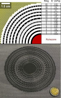
“Circling“ around the silent center: Design (top) and intermediate step of production (bottom) of the elastic invisibility cloak. (Graphics: AP, KIT)
The scientists explain their idea by the following story: A city, in the shape of a circle, suffers from noisy car traffic through its center. Finally, the mayor has the idea to introduce a speed limit for cars that drive directly towards the city: The closer the cars come to the city area, the slower they have to drive. At the same time, the mayor orders to build circular roads around the city, on which the cars are allowed to drive at higher speeds. The cars can approach the city, drive around it, and leave it in the same direction in the end. The time required corresponds to the time needed without the city. From outside, it appears as if the city was not there.

Karlsruhe Institute of Technology (KIT) is a public corporation according to the legislation of the state of Baden-Württemberg. It fulfills the mission of a university and the mission of a national research center of the Helmholtz Association. KIT focuses on a knowledge triangle that links the tasks of research, teaching, and innovation.

le, 20.12.2011 For further information, please contact: Margarete Lehné Presse, Kommunikation und Marketing Phone: +49 721 608-48121 Fax: +49 721 608-45681 margarete lehne∂kit edu

Contact: Monika Landgraf Chief Press Officer Phone: +49 721 608-47414, Fax: +49 721 608-43658 e-mail

Friday, December 30, 2011

Stand Alone MilliMeter wave Imager is able to see through all non-transparent materials

We may be able to see through glass, water and air, but not packing paper, plastic or cardboard. What remains hidden from the human eye is made visible by a new millimeter-wave sensor: unlike x-ray scanners, it can see through non-transparent materials without sending out harmful rays.

Has the packet been properly filled? Are there impurities in the chocolate? Have the plastic seams been welded correctly? Is there a knife hidden in the parcel? Answers to all these questions are provided by SAMMI, short for Stand Alone MilliMeter wave Imager. The millimeter-wave sensor is able to see through all non-transparent materials. Researchers at the Fraunhofer Institute for High Frequency Physics and Radar Techniques FHR in Wachtberg have developed the device, whichat 50 centimeters wide and 32 centimeters high is no larger than a compact laser printer. SAMMI can happily deal with all non-metallic materials.

“The system detects wooden splinters lurking in diapers, air pockets in plastic, breaks in bars of marzipan, and foreign bodies in foodstuffs. It can even detect and monitor the dehydration process in plants and how severely they have been stressed by drought,” says Dr. Helmut Essen, head of the FHR’s millimeter-wave radar and high-frequency sensors department. This makes the scanner extremely versatile – it’s just as suitable for industrial product and quality control as for analyzing materials in the laboratory. Because the system can detect dangerous substances such as explosive powder hidden in letters, vulnerable people such as politicians or freight handlers can be protected by millimeter-wave radar.

millimeter-wave sensor can look through all non-transparent, non-metallic materials

The millimeter-wave sensor can look through all non-transparent, non-metallic materials. © Fraunhofer FHR
SAMMI’s most striking feature is its ability to pick out the smallest differences in materials – differences that are invisible to x-rays. SAMMI can for example differentiate between the different fillings of chocolates, or between rubber composites that have similar or identical absorption qualities. Another advantage is that the scanner doesn’t employ ionizing radiation, which can damage health. It is also low-maintenance, not requiring the regular checks necessary with x-ray tubes.

But how does SAMMI work? Inside the system’s housing, there is both a transmitting and a receiving antenna on each of two opposing rotating plates. A conveyor belt transports the sample – perhaps a package whose contents are unknown – between the antennae, while these send electromagnetic waves in a high frequency of 78 GHz.

Different areas of the sample absorb the signal to different degrees, leading the varying material composition across a sample to show up in distinguishable contrast. “Basically we examine the scanned objects for dissimilarities,” explains Essen. The content of the sample appears in real time on the scanner’s fold-out display. If the package contains a knife, even the grain of the handle is discernible. If the handle is hollow, the millimeter-wave sensor would show that, too. The device scans an area of 30 x 30 centimeters in just 60 seconds.

Our system can be operated without safety precautions or safety instructions, and since it weighs just 20 kilograms it’s eminently portable. It can also be adjusted to various measuring frequencies,” the scientist points out. In future, the researchers aim to “upgrade” the system for terahertz frequencies of 2 THz. “Then we’ll be in a position not just to detect different structures but also to establish which type of plastic a product is made from. That’s not possible at the moment,” says Dr. Essen.

At present, SAMMI is only suitable for spot checks. However, the FHR researchers are working on adapting the millimeter-wave sensor for industrial assembly lines for the fast, automatic inspection of goods. They envision mounting a line of sensors over the conveyor belt, so that in future products can be scanned at a speed of up to six meters per second.

TEXT CREDIT: fraunhofer.de Contact: Dr. Helmut Essen Fraunhofer Institute for High Frequency Physics and Radar Techniques FHR Neuenahrer Str. 20 53343 Wachtberg, Germany Phone +49 228 9435-249. Send E-Mail

Thursday, December 29, 2011

Stable two-dimensional networks of organic molecules are important components in various nanotechnology processes

Stable two-dimensional networks of organic molecules are important components in various nanotechnology processes. However, producing these networks, which are only one atom thick, in high quality and with the greatest possible stability currently still poses a great challenge. Scientists from the Excellence Cluster Nanosystems Initiative Munich (NIM) have now successfully created just such networks made of boron acid molecules. The current issue of the scientific journal ACSnano reports on their results.

Even the costliest oriental carpets have small mistakes. It is said that pious carpet-weavers deliberately include tiny mistakes in their fine carpets, because only God has the right to be immaculate. Molecular carpets, as the nanotechnology industry would like to have them are as yet in no danger of offending the gods. A team of physicists headed by Dr. Markus Lackinger from the Technische Universität München (TUM) und Professor Thomas Bein from the Ludwig-Maximilians-Universität München (LMU) has now developed a process by which they can build up high-quality polymer networks using boron acid components.

The “carpets” that the physicists are working on in their laboratory in the Deutsches Museum München consist of ordered two-dimensional structures created by self-organized boron acid molecules on a graphite surface. By eliminating water, the molecules bond together in a one-atom thick network held together solely by chemical bonds – a fact that makes this network very stable. The regular honey-comb-like arrangement of the molecules results in a nano-structured surface whose pores can be used, for instance, as stable forms for the production of metal nano-particles.

Scanning electron microscopy image

Scanning electron microscopy image with a superimposed molecular model (photo: TUM)
The molecular carpets also come in nearly perfect models; however, these are not very stable, unfortunately. In these models the bonds between the molecules are very weak – for instance hydrogen bridge bonds or van der Waals forces. The advantage of this variant is that faults in the regular structure are repaired during the self-organization process – bad bonds are dissolved so that proper bonds can form.

However, many applications call for molecular networks that are mechanically, thermally and/or chemically stable. Linking the molecules by means of strong chemical bonds can create such durable molecule carpets. The down side is that the unavoidable weaving mistakes can no longer be corrected due to the great bonding strength.

Markus Lackinger and his colleagues have now found a way to create a molecular carpet with stable covalent bonds without significant weaving mistakes. The method is based on a bonding reaction that creates a molecular carpet out of individual boron acid molecules. It is a condensation reaction in which water molecules are released. If bonding takes place at temperatures of a little over 100°C with only a small amount of water present, mistakes can be corrected during weaving. The result is the sought after magic carpet: molecules in a stable and well-ordered one-layer structure.

Markus Lackinger’s laboratory is located in the Deutsches Museum München. There he is doing research at the Chair of Prof. Wolfgang Heckl (TUM School of Education, TU München). Prof. Bein holds a Chair at the Department of Chemistry at the LMU. The research was conducted in collaboration with Prof. Paul Knochel’s work group (LMU) and Physical Electronics GmbH, with funding by the Excellence Cluster Nanosystems Initiative Munich (NIM) and the Bavarian Research Foundation (BFS).

Publication: Synthesis of well-ordered COF monolayers: Surface growth of nanocrystalline precursors versus direct on-surface polycondensation. 
Jürgen F. Dienstmaier, Alexander M. Gigler, Andreas J. Goetz, Paul Knochel, Thomas Bein, Andrey Lyapin, Stefan Reichlmaier, Wolfgang M. Heckl, and Markus Lackinger 
ACS Nano Vol. 5, 12, 9737-9745

Contact person: Dr. Markus Lackinger. 
TUM School of Education. 
Deutsches Museum, 
Museumsinsel 1, 
D-80538 München. 
Tel: +49 (0)89 / 2179 – 605. 
Email: markus.lackinger@tum.de.

Media Relations Team Arcisstr. 19 80333 München Tel.: +49.89.289.22778 Fax: +49.89.289.23388. presse@tum.de

Tuesday, December 27, 2011

World's first fiber-coupled cryogenic radiometer that links optical fiber power measurements directly to fundamental electrical units

Researchers at the National Institute of Standards and Technology (NIST) have demonstrated a prototype device capable of absolute measurements of optical power delivered through an optical fiber.

The device is the world's first fiber-coupled cryogenic radiometer that links optical fiber power measurements directly to fundamental electrical units and national standards. It uses a microscopic forest of carbon nanotubes—the world's darkest material—to measure values that are about one-thousandth of the levels typically attained with a cryogenic radiometer lacking direct fiber input capability.* With improvements in temperature control and speed, the device could meet the needs for ultraprecise calibrations at ultralow power in telecommunications, medical devices and other industries.

Optical power and energy are traceable to fundamental electrical units. Radiometers absorb optical energy and convert it to heat. Then the electrical power needed to induce the same temperature increase is measured. Because optical and electrical heating are not exactly equivalent, measurement uncertainties can be relatively large from a metrology point of view.

The demonstration is also a step toward converting radiometry from a classical practice based on electrical units to a quantum practice based on single particles of light (photons).

"We have many customers who request optical power measurements in fiber, mainly for optical communications," project leader John Lehman says. "Also, our single-photon measurements are done in fiber."

Prototype NIST Device Measures Absolute Optical Power in Fiber at Nanowatt Levels

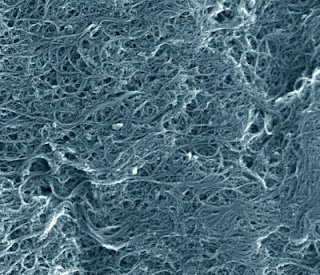
Caption: This is a colorized micrograph of multi-walled carbon nanotubes, each 40 micrometers long, which absorb more than 99.9 percent of the light inside NIST’s prototype fiber-coupled radiometer.

Credit: Huang / NanoLab, colorized by Talbott / NIST. Usage Restrictions: None.
The new radiometer is about 70 millimeters (mm) long and incorporates a 1.45-mm-thick optical fiber capped by a light-trapping cavity at one end with the nanotube absorber and a heater. The ultra-dark nanotubes** are grown on a tiny X-shaped piece of micromachined silicon. Light absorption was so high it was difficult to determine measurement uncertainties; Lehman travelled to a special facility at the National Physical Laboratory (the British equivalent of NIST) to make some measurements.

Experiments and calculations indicate the new radiometer can measure a power level of 10 nanowatts with an uncertainty of 0.1 percent. By comparison, typical measurements of optical power delivered through fiber have an uncertainty of 3 percent or more at similar power levels. More importantly, these commercial devices rely on a series of calibrations to establish traceability to national standards.

NIST aims to develop an absolute quantum standard for optical power and energy based on single photons. The effort includes development of sources and detectors spanning a wide range of optical power measurements, from single photon counts to trillions of photons. Single photons are already used in quantum communications systems, which offer novel capabilities such as detecting extremely weak optical signals and providing quantum guarantees on security.
###

* D. Livigni, N. Tomlin, C.L. Cromer and J.H. Lehman. Fiber-coupled cryogenic radiometer with carbon nanotube absorber. Paper presented at 11th International Conference on New Show allDevelopments and Applications in Optical Radiometry (NEWRAD 2011), Maui, Hawaii, Sept. 19-23, 2011.

D.J. Livigni, N.A. Tomlin, C.L. Cromer and J.H. Lehman. Optical fiber-coupled cryogenic radiometer with carbon nanotube absorber. Metrologia. Forthcoming.

** See the 2010 NIST Tech Beat article, "Extreme Darkness: Carbon Nanotube Forest Covers NIST's Ultra-dark Detector" at www.nist.gov/pml/div686/dark_081710.

Contact: Laura Ost laura.ost@nist.gov 303-497-4880 National Institute of Standards and Technology (NIST)

Monday, December 26, 2011

(NIST) has issued the world's first reference material for single-wall carbon nanotube soot

The National Institute of Standards and Technology (NIST) has issued the world's first reference material for single-wall carbon nanotube soot. Distantly related to the soot in your fireplace or in a candle flame, nanotube-laden soot is the primary industrial source of single-wall carbon nanotubes, perhaps the archetype of all nanoscale materials. The new NIST material offers companies and researchers a badly needed source of uniform and well-characterized carbon nanotube soot for material comparisons, as well as chemical and toxicity analysis.

With walls of carbon only one atom thick and looking like a sheet of chicken wire curled into a cylinder, single-wall carbon nanotubes are one of several families of pure carbon materials that, because of their nanoscale size, have special properties. "Single-wall carbon nanotubes," says NIST chemical engineer Jeffery Fagan, "have exquisite optical, mechanical, thermal and electronic properties, and because of their small width but long lengths—think of something like a long piece of hair but 10,000 times thinner—full development of these materials should enable lighter, stronger materials, as well as improve many technologies from sensors to electronics and batteries."

Unfortunately, nanotubes are difficult to produce without significant impurities or in large quantities. Single-wall nanotubes, in particular, have been notorious for their relatively low quality and batch-to-batch variability. They typically are produced in complex processes using small particles of metal catalysts that promote the growth of the nanotubes. The resulting material—often a powder not unlike the soot you would find in your fireplace—has frequently contained large amounts of impurities, such as other forms of carbon, and sometimes significant levels of catalysts.

Single-Wall Carbon Nanotubes

Caption: This is a scanning electron microscope image of a typical sample of the NIST single-wall carbon nanotube soot standard reference material. The nanotubes tend to stick together and form smaller and larger bundles. Some of the impurities also are visible. The image shows an area just over a micrometer wide. (Color added for clarity.)

Credit: Vladar, NIST. Usage Restrictions: None.
"One of the issues that this reference material addresses is that there's no homogeneous lot that people can buy to do comparative measurements," says Fagan. "Even batch-to-batch, raw carbon nanotube powder samples have varied so much that there is no interlaboratory consistency. And that's particularly a problem for comparisons such as toxicity measurements. If you bought carbon nanotubes, you were pretty much guaranteed that your sample could be so different from anyone else's samples that either your measurements could be specific to some flaw of your material, or that others might not be able to reproduce what you were doing."

To address these issues, a multidisciplinary research team at NIST has worked to develop the metrology necessary for quantitative single-wall carbon nanotube measurements through a three-prong approach: basic measurement and separation science, documentary protocols and standards through international standards organizations, and now certified reference materials.

The new NIST product, Standard Reference Material (SRM) 2483, "Single-Wall Carbon Nanotubes (Raw Soot)," will directly address the issue of comparability. It is possibly the world's single largest supply of homogeneous, chemically analyzed, carbon nanotube soot where the uniformity of the samples from unit to unit is assured. Each unit of SRM 2483, a glass vial containing 250 milligrams of soot, is certified by NIST for the mass fraction values of several common contaminants: barium, cerium, chlorine, cobalt, dysprosium, europium, gadolinium, lanthanum, molybdenum and samarium. Reference values (values believed to be accurate, but not rising to the level of confidence that NIST certifies) are provided for an additional seven elements.

NIST also provides additional reference data useful for nanotube analysis, including thermal gravimetric and Raman data, as well as informational values for ultraviolet-visible-near-infrared absorbance spectra, near-infrared fluorescence spectra, Raman scattering spectra and scanning electron microscopy images. With these sets of information, purchasers of the material should be able to compare their results against the NIST values and against those from suppliers or after processing, ensuring a consistent point of comparison.

###

Single units of SRM 2483, "Single-Wall Carbon Nanotubes (Raw Soot)," are available from the NIST Standard Reference Materials Program at https://www.nist.gov/srm/. See https://www-s.nist.gov/srmors/view_detail.cfm?srm=2483 for details.

Standard Reference Materials are among the most widely distributed and used products from NIST. The agency prepares, analyzes and distributes more than a thousand different materials that are used throughout the world to check the accuracy of instruments and test procedures used in manufacturing, clinical chemistry, environmental monitoring, electronics, criminal forensics and dozens of other fields.

Contact: Michael Baum baum@nist.gov 301-975-2763 National Institute of Standards and Technology (NIST)

Sunday, December 25, 2011

All-silicon passive optical diode, small enough to fit millions on a chip, faster, more powerful information processing and supercomputers

WEST LAFAYETTE, Ind. - Researchers have created a new type of optical device small enough to fit millions on a computer chip that could lead to faster, more powerful information processing and supercomputers.

The "passive optical diode" is made from two tiny silicon rings measuring 10 microns in diameter, or about one-tenth the width of a human hair. Unlike other optical diodes, it does not require external assistance to transmit signals and can be readily integrated into computer chips.

The diode is capable of "nonreciprocal transmission," meaning it transmits signals in only one direction, making it capable of information processing, said Minghao Qi (pronounced Chee), an associate professor of electrical and computer engineering at Purdue University.

"This one-way transmission is the most fundamental part of a logic circuit, so our diodes open the door to optical information processing," said Qi, working with a team also led by Andrew Weiner, Purdue's Scifres Family Distinguished Professor of Electrical and Computer Engineering.

The diodes are described in a paper to be published online Thursday (Dec. 22) in the journal Science. The paper was written by graduate students Li Fan, Jian Wang, Leo Varghese, Hao Shen and Ben Niu, research associate Yi Xuan, and Weiner and Qi.

Although fiberoptic cables are instrumental in transmitting large quantities of data across oceans and continents, information processing is slowed and the data are susceptible to cyberattack when optical signals must be translated into electronic signals for use in computers, and vice versa.


all-silicon passive optical diode

This illustration shows a new "all-silicon passive optical diode," a device small enough to fit millions on a computer chip that could lead to faster, more powerful information processing and supercomputers. The device has been developed by Purdue University researchers. (Birck Nanotechnology Center, Purdue University)
"This translation requires expensive equipment," Wang said. "What you'd rather be able to do is plug the fiber directly into computers with no translation needed, and then you get a lot of bandwidth and security."

Electronic diodes constitute critical junctions in transistors and help enable integrated circuits to switch on and off and to process information. The new optical diodes are compatible with industry manufacturing processes for complementary metal-oxide-semiconductors, or CMOS, used to produce computer chips, Fan said.

"These diodes are very compact, and they have other attributes that make them attractive as a potential component for future photonic information processing chips," she said.

The new optical diodes could make for faster and more secure information processing by eliminating the need for this translation. The devices, which are nearly ready for commercialization, also could lead to faster, more powerful supercomputers by using them to connect numerous processors together.

"The major factor limiting supercomputers today is the speed and bandwidth of communication between the individual superchips in the system," Varghese said. "Our optical diode may be a component in optical interconnect systems that could eliminate such a bottleneck."

Infrared light from a laser at telecommunication wavelength goes through an optical fiber and is guided by a microstructure called a waveguide. It then passes sequentially through two silicon rings and undergoes "nonlinear interaction" while inside the tiny rings. Depending on which ring the light enters first, it will either pass in the forward direction or be dissipated in the backward direction, making for one-way transmission. The rings can be tuned by heating them using a "microheater," which changes the wavelengths at which they transmit, making it possible to handle a broad frequency range.

###

The work was performed in laboratories operated by the Birck Nanotechnology Center in Purdue's Discovery Park and by the School of Electrical and Computer Engineering. It was funded by the U.S. Defense Threat Reduction Agency, Air Force Office of Scientific Research, National Science Foundation and the National Institutes of Health. Simulation work was carried out through the Network for Computational Nanotechnology (NCN), with resources available at www.nanohub.org.

Contact: Purdue University Writer: Emil Venere, 765-494-4709, venere@purdue.edu, Sources: Minghao Qi, 765 494-3646, mqi@purdue.edu, Andrew Weiner, 765-494-5574, amw@purdue.edu

Saturday, December 24, 2011

More contrast between tumors and healthy tissue, doctors apply nanoparticles containing iron oxide, improves MRI images

PHILADELPHIA — Many imaging technologies and their contrast agents — chemicals used during scans to help detect tumors and other problems — involve exposure to radiation or heavy metals, which present potential health risks to patients and limit the ways they can be applied. In an effort to mitigate these drawbacks, new research from University of Pennsylvania engineers shows a way to coat an iron-based contrast agent so that it only interacts with the acidic environment of tumors, making it safer, cheaper and more effective than existing alternatives.

The research was conducted by associate professor Andrew Tsourkas and graduate student Samuel H. Crayton of the department of bioengineering in Penn's School of Engineering and Applied Science. It was published in the journal ACS Nano.

Magnetic resonance imaging, or MRI, is an increasingly common feature of medical care. Using a strong magnetic field to detect and influence the alignment of water molecules in the body, MRI can quickly produce pictures of wide range of bodily tissues, though the clarity of these pictures is sometimes insufficient for diagnoses. To improve the differentiation — or contrast — between tumors and healthy tissue, doctors can apply a contrast agent, such as nanoparticles containing iron oxide. The iron oxide can improve MRI images due to their ability to distort the magnetic field of the scanner; areas they are concentrated in stand out more clearly.

These nanoparticles, which have recently been approved in the United States for clinical use as contrast agents, are literally sugar-coated; an outer layer of dextran keeps the particles from binding or being absorbed by the body and potentially sickening the patient. This non-reactive coating allows the iron oxide to be flushed out after the imaging is complete, but it also means that the particles can't be targeted to a particular kind of tissue.

tumor, indicated by the white arrow, is darkened by a glycol chitosan contrast agent
A tumor, indicated by the white arrow, is darkened by a glycol chitosan contrast agent.
If the contrast agent could be engineered so it only sticks to tissue that is already diseased, such as tumors, it would solve both problems at once. Scientists have tried this approach by coating nanoparticles with proteins that bind only to receptors found on the exterior of tumors, but not all tumors are the same in this regard.

"One of the limitations of a receptor-based approach is that you just don't hit everything," Tsourkas said. "It's hard to recommend them as a screening tool when you know that the target receptors are only expressed in 30% of tumors."

"One of the reasons we like our approach is that it hits a lot of tumors; almost all tumors exhibit a change in the acidity of their microenvironment."

The Penn engineers took advantage of something known as the Warburg effect, a quirk of tumor metabolism, to get around the targeting problem. Most of the body's cells are aerobic; they primarily get their energy from oxygen. However, even when oxygen is plentiful, cancerous cells use an anaerobic process for their energy. Like overtaxed muscles, they turn glucose into lactic acid, but unlike normal muscles, tumors disrupt the blood flow around them and have a hard time clearing this acid away. This means that tumors almost always have a lower pH than surrounding healthy tissue.

Some imaging technologies, such as magnetic resonance spectroscopy, can also take advantage of tumors' low-pH microenvironments, but they require expensive specialized equipment that is not available in most clinical settings.

By using glycol chitosan — a sugar-based polymer that reacts to acids — the engineers allowed the nanocarriers to remain neutral when near healthy tissue, but to become ionized in low pH. The change in charge that occurs in the vicinity of acidic tumors causes the nanocarriers to be attracted to and retained at those sites.

This approach has another benefit: the more malignant a tumor is, the more it disrupts surrounding blood vessels and the more acidic its environment becomes. This means that the glycol chitosan-coated is a good detector of malignancy, opening up treatment options above and beyond diagnosis.

"You can take any nanoparticle and put this coating on it, so it's not limited to imaging by any means," said Tsourkas. "You could also use it to deliver drugs to tumor sites."

The researchers hope that, within seven to 10 years, glycol-chitosan-coated iron oxide nanoparticles could improve the specificity of diagnostic screening. The ability to accurately detect sites of malignancy by MRI would be an immediate improvement to existing contrast agents for certain breast cancer scans.

"Gadolinium is used as a contrast agent in MRI breast cancer screenings for high-risk patients. These patients are recommended to get an MRI in addition to the usual mammogram, because the sensitivity of mammograms can be poor," said Tsourkas. "The sensitivity of an MRI is much higher, but the specificity is low: the screening detects a lot of tumors, but many of them are benign. Having a tool like ours would allow clinicians to better differentiate the benign and malignant tumors, especially since there has been shown to be a correlation between malignancy and pH."

###

The research was supported by the National Institutes of Health and the Department of Defense Breast Cancer Research Program.

Contact: Evan Lerner elerner@upenn.edu 215-573-6604 University of Pennsylvania

Friday, December 23, 2011

plasmonic nanoantennas manipulate light in new ways that could make possible a range of optical innovations

WEST LAFAYETTE, Ind. – Researchers have shown how arrays of tiny "plasmonic nanoantennas" are able to precisely manipulate light in new ways that could make possible a range of optical innovations such as more powerful microscopes, telecommunications and computers.

The researchers at Purdue University used the nanoantennas to abruptly change a property of light called its phase. Light is transmitted as waves analogous to waves of water, which have high and low points. The phase defines these high and low points of light.

"By abruptly changing the phase we can dramatically modify how light propagates, and that opens up the possibility of many potential applications," said Vladimir Shalaev, scientific director of nanophotonics at Purdue's Birck Nanotechnology Center and a distinguished professor of electrical and computer engineering.

Findings are described in a paper to be published online Thursday (Dec. 22) in the journal Science.

The new work at Purdue extends findings by researchers led by Federico Capasso, the Robert L. Wallace Professor of Applied Physics and Vinton Hayes Senior Research Fellow in Electrical Engineering at the Harvard School of Engineering and Applied Sciences. In that work, described in an October Science paper, Harvard researchers modified Snell's law, a long-held formula used to describe how light reflects and refracts, or bends, while passing from one material into another.

"What they pointed out was revolutionary," Shalaev said.

plasmonic nanoantennas

The image in the upper left shows a schematic for an array of gold "plasmonic nanoantennas" able to precisely manipulate light in new ways, a technology that could make possible a range of optical innovations such as more powerful microscopes, telecommunications and computers. At upper right is a scanning electron microscope image of the structures. The figure below shows the experimentally measured refraction angle versus incidence angle for light, demonstrating how the nanoantennas alter the refraction. (Purdue University Birck Nanotechnology Center image)
Until now, Snell's law has implied that when light passes from one material to another there are no abrupt phase changes along the interface between the materials. Harvard researchers, however, conducted experiments showing that the phase of light and the propagation direction can be changed dramatically by using new types of structures called metamaterials, which in this case were based on an array of antennas.

The Purdue researchers took the work a step further, creating arrays of nanoantennas and changing the phase and propagation direction of light over a broad range of near-infrared light. The paper was written by doctoral students Xingjie Ni and Naresh K. Emani, principal research scientist Alexander V. Kildishev, assistant professor Alexandra Boltasseva, and Shalaev.

The wavelength size manipulated by the antennas in the Purdue experiment ranges from 1 to 1.9 microns.

"The near infrared, specifically a wavelength of 1.5 microns, is essential for telecommunications," Shalaev said. "Information is transmitted across optical fibers using this wavelength, which makes this innovation potentially practical for advances in telecommunications."

The Harvard researchers predicted how to modify Snell's law and demonstrated the principle at one wavelength.

"We have extended the Harvard team's applications to the near infrared, which is important, and we also showed that it's not a single frequency effect, it's a very broadband effect," Shalaev said. "Having a broadband effect potentially offers a range of technological applications."

The innovation could bring technologies for steering and shaping laser beams for military and communications applications, nanocircuits for computers that use light to process information, and new types of powerful lenses for microscopes.

Critical to the advance is the ability to alter light so that it exhibits "anomalous" behavior: notably, it bends in ways not possible using conventional materials by radically altering its refraction, a process that occurs as electromagnetic waves, including light, bend when passing from one material into another.

Scientists measure this bending of radiation by its "index of refraction." Refraction causes the bent-stick-in-water effect, which occurs when a stick placed in a glass of water appears bent when viewed from the outside. Each material has its own refraction index, which describes how much light will bend in that particular material. All natural materials, such as glass, air and water, have positive refractive indices.

However, the nanoantenna arrays can cause light to bend in a wide range of angles including negative angles of refraction.

"Importantly, such dramatic deviation from the conventional Snell's law governing reflection and refraction occurs when light passes through structures that are actually much thinner than the width of the light's wavelengths, which is not possible using natural materials," Shalaev said. "Also, not only the bending effect, refraction, but also the reflection of light can be dramatically modified by the antenna arrays on the interface, as the experiments showed."

The nanoantennas are V-shaped structures made of gold and formed on top of a silicon layer. They are an example of metamaterials, which typically include so-called plasmonic structures that conduct clouds of electrons called plasmons. The antennas themselves have a width of 40 nanometers, or billionths of a meter, and researchers have demonstrated they are able to transmit light through an ultrathin "plasmonic nanoantenna layer" about 50 times smaller than the wavelength of light it is transmitting.

"This ultrathin layer of plasmonic nanoantennas makes the phase of light change strongly and abruptly, causing light to change its propagation direction, as required by the momentum conservation for light passing through the interface between materials," Shalaev said.

###

The work has been funded by the U.S. Air Force Office of Scientific Research and the National Science Foundation's Division of Materials Research.

Contact: Emil Venere venere@purdue.edu 765-494-4709 Purdue University

Wednesday, December 21, 2011

"solar paint" that uses semiconducting nanoparticles to produce energy.VIDEO

Imagine if the next coat of paint you put on the outside of your home generates electricity from light—electricity that can be used to power the appliances and equipment on the inside.

A team of researchers at the University of Notre Dame have made a major advance toward this vision by creating an inexpensive "solar paint" that uses semiconducting nanoparticles to produce energy.

"We want to do something transformative, to move beyond current silicon-based solar technology," says Prashant Kamat, John A. Zahm Professor of Science in Chemistry and Biochemistry and an investigator in Notre Dame's Center for Nano Science and Technology (NDnano), who leads the research.

"By incorporating power-producing nanoparticles, called quantum dots, into a spreadable compound, we've made a one-coat solar paint that can be applied to any conductive surface without special equipment."

The team's search for the new material, described in the journal ACS Nano, centered on nano-sized particles of titanium dioxide, which were coated with either cadmium sulfide or cadmium selenide. The particles were then suspended in a water-alcohol mixture to create a paste.

When the paste was brushed onto a transparent conducting material and exposed to light, it created electricity.

"The best light-to-energy conversion efficiency we've reached so far is 1 percent, which is well behind the usual 10 to 15 percent efficiency of commercial silicon solar cells," explains Kamat.

Painting Solar Cells with Nanoparticle Paste


"But this paint can be made cheaply and in large quantities. If we can improve the efficiency somewhat, we may be able to make a real difference in meeting energy needs in the future."

"That's why we've christened the new paint, Sun-Believable," he adds.

Kamat and his team also plan to study ways to improve the stability of the new material.

NDnano is one of the leading nanotechnology centers in the world. Its mission is to study and manipulate the properties of materials and devices, as well as their interfaces with living systems, at the nano-scale.

###

This research was funded by the Department of Energy's Office of Basic Energy Sciences.

Contact: Prashant Kamat pkamat@nd.edu 574-631-5411 University of Notre Dame

Tuesday, December 20, 2011

Unusual heat-transfer properties of boron nanoribbon bundles can be modified

Boron nanoribbons reveal surprising thermal properties in bundles Size matters… but apparently so does shape – when it comes to conducting heat in very small spaces.

Researchers looking at the thermal conductivity of boron nanoribbons have found that they have unusual heat-transfer properties when compared to other wire/tube-like nanomaterials. While past experiments have shown that bundles of non-metallic nanostructures are less effective in conducting heat energy than single nanostructures, a new study shows that bundling boron nanoribbons can have the opposite effect and "the thermal conductivity of a bundle of boron nanoribbons can be significantly higher than that of a single free-standing nanoribbon," according to a report in Nature Nanotechnology, published online on December 11.

The finding is the result of work by a multidisciplinary team headed by Ravi Prasher of the Advanced Research Projects Agency, Terry Xu of the University of North Carolina at Charlotte, and Deyu Li of Vanderbilt University (see a complete list of authors below).

Additionally, the researchers found that the unusual heat-transfer properties of boron nanoribbon bundles can be modified, allowing the higher thermal conductivity to be switched on and off through relatively simple physical manipulation. The study concludes that the ribbon structure of the nanomaterials is strongly related to the unusual thermal conductivity of the bundles.

Boron-based nanostructures are a promising class of high temperature thermoelectric materials -- substances that can convert waste heat to useful electricity – and thermal conductivity is related to other thermoelectric properties. Physicists describe the transmission of heat energy in materials like boron as happening through the conduction of "phonons," quasi-wave-particles that carry energy through excitations of the material's atoms.

Terry Xu

Nanomaterials, devices & fabrication Assistant Professor 256 Duke Hall, UNC Charlotte 704-687-8353 ttxu@uncc.edu
"What we found was largely unexpected," said Xu. "When two nanoribbons were put together, the thermal conductivity was found to rise significantly rather than staying the same or going down, as has been the case in previous measurements. It has been assumed that phonons were hampered by the interface between the individual nanostructures in similar materials.

"That seems to mean that the phonon can pass effectively through the interface between two boron nanoribbons," she said. "The question is whether or not this result is due to the weak van der Waals interactions between two nanostructures of ultra-flat geometry."

The team suspects that the reason for the enhanced thermal conductivity is due in large part to the flat surface structure of the nanoribbons, based on another experimental result that the group discovered by accident.

The nanoribbon bundles exhibiting the unexpectedly higher thermal conductivity were originally prepared in a solution of reagent alcohol and water, which was then allowed to evaporate, leaving some nanoribbons drawn together by van der Waals force (the weak attraction that non reactive and uncharged substances can have for each other). When other members of the team attempted to duplicate this result, however, the experiment failed and the bundles only had the lower thermal conductivity of single ribbons. The researchers then noted that a significant difference between the two attempts was that the second experiment had used isopropyl alcohol rather than reagent alcohol in the solution. Since isopropyl alcohol was known to leave minute residue following evaporation, the researchers suspected that a residue was forming on the ribbons surfaces – a fact that microscopy confirmed -- and the residue apparently prevented tight contact between two nanoribbons. Further tests were made on the lower-conducting bundles, where the ribbon interfaces were washed with reagent alcohol to remove the isopropyl residue, and in this experiment the higher thermal conductivity was achieved.

The results point to the conclusion that boron nanoribbons form better heat-conducting bundles because the ribbons flat surfaces allow for tighter, more complete contact between the individual structures through van der Waals interaction and improved transmission of phonons overall.

"The result implies that achieving a tight van der Waals interface between the ribbons is important in thermal conductivity, something their geometry encourages," Xu said. "It is possible that this result may have implications for other materials with ribbon-based nanostructures."

Xu notes that there are potential engineering applications for the finding come not just from the improved thermal conductivity of boron nanoribbon bundles, but also from the reversible nature of the effect.

"This may lead to a simple way to switch the thermal conductivity of the bundle on and off," she said. "If you want more heat dissipated, but only in certain conditions, you can apply a solution to create a bundle structure with tight bonds and higher thermal conductivity. It could similarly be reversed by adding a residue between the nanoribbons and reducing the thermal conductivity to that of an individual ribbon."

###

The finding appears in a letter to Nature Nanotechnology. The authors are Juekuan Yang, Yang Yang, Scott Waltermire and Deyu Li from Vanderbilt University; Xiaoxia Wu, Haitao Zhang, Timothy Gutu, Youfei Jiang, and Terry Xu from UNC Charlotte; Yunfei Chen from Southwest University in Nanjing, China; Alfred Zinn from Lockheed Martin Space Systems and Ravi Prasher from the Advanced Research Projects Agency in the US Department of Energy. This research was funded by the National Science Foundation and Lockheed Martin.

Contact: James Hathaway jbhathaw@uncc.edu 704-687-5743 University of North Carolina at Charlotte

Sunday, December 18, 2011

Tissue Engineering creation of new polymer scaffolds which guide new nerve growth VIDEO

Professor John Haycock takes an in-depth look at the problem of repairing peripheral nerve damage. Approximately 1 in 1000 people suffers serious nerve injuries due to road traffic or DIY accidents each year. Repairing this nerve damage surgically can be difficult as clean cuts are rare. The specialist team at Sheffield is overcoming this problem through the creation of new polymer scaffolds which guide new nerve growth, assist repair and provide an 'off the shelf' solution for surgeons.

Category: Science & Technology

Tags: Biomaterials, tissue engineering, cell cultures, nerve guides, nerve damage, polymer nanotechnology, medical device, repairing body parts, clean rooms, Healthcare, University of Sheffield, research, researchatsheffield, laboratories

License: Standard YouTube License

Professor John W Haycock, Dr J W Haycock BSc (Hons) PhD. Professor of Bioengineering. Director – Centre for Biomaterials & Tissue Engineering. Associate Director – Kroto Research Institute

Address: The Kroto Research Institute, North Campus, University of Sheffield. Broad Lane, Sheffield S3 7HQ. Telephone: +44 (0) 114 222 5972, Fax: +44 (0) 114 222 5943, Email: j.w.haycock@sheffield.ac.uk

John Haycock is a Professor in the Department Materials Science & Engineering, Associate Director of the Kroto Research Institute and Director of the Centre for Biomaterials & Tissue Engineering. He joined the department in 2001 from the Medical School at Sheffield University where he was a Research Fellow. He obtained his first degree and PhD in Biochemistry at Newcastle University and was a PDRA at Albany Medical College in New York. His research group is based in the Kroto Research Institute.


John is also Course Director for the B.Eng/M.Eng (Hons) Biomaterial Science Tissue Engineering degree programme and Admissions Tutor for the new B.Eng/M.Eng (Hons) Bioengineering degree programme at Sheffield, being launched in 2011.

Professor John W Haycock

VIDEO and IMAGE CREDIT: ResearchatSheffield

TEXT RESOURCE: Professor John W Haycock

Saturday, December 17, 2011

Nanomechanical oscillator used for detection and amplification of radio or micro waves

Physicists in Low Temperature Laboratory of Aalto University have shown how a nanomechanical oscillator can be used for detection and amplification of feeble radio waves or microwaves.

A measurement using such a tiny device, resembling a miniaturized guitar string, can be performed with the least possible disturbance. The results were recently published in the most prestigious scientific arena, the British journal Nature.

The researchers cooled the nanomechanical oscillator, thousand times thinner than a human hair, down to a low temperature near the absolute zero at -273 centigrade. Under such extreme conditions, even nearly macroscopic sized objects follow the laws of quantum physics which often contradict common sense. In the Low Temperature Laboratory experiments, the nearly billion atoms comprising the nanomechanical resonator were oscillating in pace in their shared quantum state.

The scientists had fabricated the device in contact with a superconducting cavity resonator, which exchanges energy with the nanomechanical resonator. This allowed amplification of their resonant motion. This is very similar to what happens in a guitar, where the string and the echo chamber resonate at the same frequency. Instead of the musician playing the guitar string, the energy source was provided by a microwave laser.

Microwaves get amplified by interaction of quantum oscillations

Researchers from the Low Temperature Laboratory, Aalto University, have shown how to detect and amplify electromagnetic signals almost noiselessly using a guitar-string like mechanical vibrating wire. In the ideal case the method adds only the minimum amount of noise required by quantum mechanics.

nanomechanical microwave amplifier

nanomechanical microwave amplifier

The presently used semiconductor transistor amplifiers are complicated and noisy devices, and operate far away from a fundamental disturbance limit set by quantum physics. The Low Temperature Laboratory scientists showed that by taking advantage of the quantum resonant motion, injected microwave radiation can be amplified with little disturbance. The principle hence allows for detecting much weaker signals than usually.

̶ Any measurement method or device always adds some disturbance. Ideally, all the noise is due vacuum fluctuations predicted by quantum mechanics. In theory, our principle reaches this fundamental limit. In the experiment, we got very close to this limit, says Dr. Francesco Massel.

̶ The discovery was actually quite unexpected. We were aiming to cool the nanomechanical resonator down to its quantum ground state. The cooling should manifest as a weakening of a probing signal, which we observed. But when we slightly changed the frequency of the microwave laser, we saw the probing signal to strengthen enormously. We had created a nearly quantum limited microwave amplifier, says Academy Research Fellow Mika Sillanpää who planned the project and made the measurements.

Certain real-life applications will benefit from the better amplifier based on the new Aalto method, but reaching this stage requires more research effort. Most likely, the mechanical microwave amplifier will be first applied in related basic research, which will further expand our knowledge of the borderline between the everyday world and the quantum realm.

According to Academy Research Fellow Tero Heikkilä, the beauty of the amplifier is in its simplicity: it consists of two coupled oscillators. Therefore, the same method can be realized in basically any media. By using a different structure of the cavity, one could detect terahertz radiation which would also be a major application.

The research was carried out in the Low Temperature Laboratory, which belongs to the Aalto University School of Science, and is part of the Centre of Excellence in Low Temperature Quantum Phenomena and Devices of the Finnish Academy. The devices used in the measurements were fabricated by VTT Nanotechnologies and microsystems. The research was funded by the Finnish Academy, European Research Council ERC, and the European Union.

Further information:

Contact: Kim Luke kim.luke@utoronto.ca 416-978-4352 University of Toronto

Mika Sillanpää Aalto University School of Science Mika.Sillanpaa@aalto.fi tel. +358 9 470 24898

Tero Heikkilä Aalto University School of Science Tero.Heikkila@aalto.fi tel. +358 9 470 22396

Francesco Massel Aalto University School of Science Francesco.Massel@aalto.fi
puh. +358 50 3015566

Friday, December 16, 2011

DNA detection laser transmission spectroscopy

A team of researchers from the University of Notre Dame have demonstrated a novel DNA detection method that could prove suitable for many real-world applications.

Physicists Carol Tanner and Steven Ruggiero led the team in the application of a new technique called laser transmission spectroscopy (LTS). LTS is capable of rapidly determining the size, shape and number of nanoparticles in suspension.

In a new paper appearing in the international, peer-reviewed, open-access, online publication PLoS ONE, the team describes how they applied LTS as a novel method for detecting species-specific DNA where the presence of one invasive species was differentiated from a closely related invasive sister species.

The research was carried out in support of and cooperation with Notre Dame's Environmental Change Initiative (ECI). Scientists from ECI are using environmental DNA (eDNA) as part of their surveillance of Asian carp in the Great Lakes region.

The results of the research demonstrate the basic premise of DNA detection by LTS in the laboratory.

The Notre Dame research team points out that the LTS technique has many benefits over established DNA detection techniques. The technique is highly sensitive and takes only a few seconds to genetically score a sample for species presence or absence. The researchers also feel that LTS technology will prove much more rapid, practical and cost effective than current detection methodologies and could ultimately reach the sensitivity required to eliminate the need for polymerase chain reaction (PCR) amplification.

Physicists Carol Tanner and Steven Ruggiero

Physicists Carol Tanner and Steven Ruggiero.
Although the current paper describes the use of LTS is invasive species detection, the Notre Dame researchers believe that the technique could serve as an important tool in detecting human pathogens and understanding and indicating the presence of genetic diseases such as cancer.

The Notre Dame group is investigating the real-world applications of LTS technology generally and working on transitioning its success from the lab to the field.

###

Contact: Carol Tanner ctanner@nd.edu 574-631-8369 University of Notre Dame

Wednesday, December 14, 2011

Realizing Visible-Light-Induced Self-Cleaning Property of Cotton through Coating N-TiO2 Film and Loading AgI Particles

Imagine jeans, sweats or socks that clean and de-odorize themselves when hung on a clothesline in the sun or draped on a balcony railing. Scientists are reporting development of a new cotton fabric that does clean itself of stains and bacteria when exposed to ordinary sunlight. Their report appears in the ACS’ journal Applied Materials & Interfaces.

Mingce Long and Deyong Wu say their fabric uses a coating made from a compound of titanium dioxide, the white material used in everything from white paint to foods to sunscreen lotions. Titanium dioxide breaks down dirt and kills microbes when exposed to some types of light. It already has found uses in self-cleaning windows, kitchen and bathroom tiles, odor-free socks and other products. Self-cleaning cotton fabrics have been made in the past, the authors note, but they self-clean thoroughly only when exposed to ultraviolet rays. So they set out to develop a new cotton fabric that cleans itself when exposed to ordinary sunlight.

Their report describes cotton fabric coated with nanoparticles made from a compound of titanium dioxide and nitrogen. They show that fabric coated with the material removes an orange dye stain when exposed to sunlight. Further dispersing nanoparticles composed of silver and iodine accelerates the discoloration process. The coating remains intact after washing and drying.

###

The authors acknowledge funding from Donghua University and the National Natural Science Foundation of China.

visible-light-induced self-cleaning property of cotton

The visible-light-induced self-cleaning property of cotton has been realized by coating N-TiO2 film and loading AgI particles simultaneously.

The American Chemical Society is a non-profit organization chartered by the U.S. Congress. With more than 163,000 members, ACS is the world's largest scientific society and a global leader in providing access to chemistry-related research through its multiple databases, peer-reviewed journals and scientific conferences. Its main offices are in Washington, D.C., and Columbus, Ohio.

Contact: Michael Bernstein m_bernstein@acs.org 202-872-6042 American Chemical Society

Tuesday, December 13, 2011

Nanoparticles steroids offer potential treatment for macular degeneration and retinitis pigmentosa

Nanoparticles help researchers deliver steroids to retina; research at Wayne State University, Mayo Clinic and Johns Hopkins offers potential treatment for macular degeneration and retinitis pigmentosa

DETROIT — Hitching a ride into the retina on nanoparticles called dendrimers offers a new way to treat age-related macular degeneration and retinitis pigmentosa. A collaborative research study among investigators at Wayne State University, the Mayo Clinic and Johns Hopkins Medicine shows that steroids attached to the dendrimers targeted the damage-causing cells associated with neuroinflammation, leaving the rest of the eye unaffected and preserving vision.

The principal authors of the study, Raymond Iezzi, M.D. (Mayo Clinic ophthalmologist) and Rangaramanujam Kannan, Ph.D. (faculty of ophthalmology at The Wilmer Eye Institute of Johns Hopkins) have developed a clinically relevant, targeted, sustained-release drug delivery system using a simple nanodevice construct. The experimental work in rat models was initiated and substantially conducted at Wayne State University, and showed that one intravitreal administration of the nanodevice in microgram quantities could offer neuroprotection at least for a month, and appears in the journal, Biomaterials (33(3), 979-988).

Both dry age-related macular degeneration and retinitis pigmentosa are caused by neuroinflammation, which progressively damages the retina and can lead to blindness. Macular degeneration is the primary cause of vision loss in older Americans, affecting more than 7 million people, according to the National Institutes of Health. Retinitis pigmentosa encompasses many genetic conditions affecting the retina and impacts 1 in 4,000 Americans, the NIH estimates.

Nanoparticles help researchers deliver steroids to retina“There is no cure for these diseases, said Iezzi. “An effective treatment could offer hope to hundreds of millions of patients worldwide. We tested the dendrimer delivery system in rats that develop neuroinflammation leading to retinal degeneration. The target was activated microglial cells, the immune cells in charge of cleaning up dead and dying material in the eye. When activated, these cells cause damage via neuroinflammation — a hallmark of each disease.”

"Dendrimers are tree-like, non-cytotoxic polymeric drug delivery vehicles (~ 4 nm). Surprisingly, the activated microglia in the degenerating retina appeared to eat the dendrimer selectively and retain them for at least a month. The drug is released from the dendrimer in a sustained fashion inside these cells, offering targeted neuroprotection to the retina," said Kannan.

The treatment reduced neuroinflammation in the rat model and protected vision by preventing injury to photoreceptors in the retina. Although the steroid offers only temporary protection, the treatment as a whole provides sustained relief from neuroinflammation, the study found. The researchers believe that this patent-pending technology with significant translational potential will be advanced further, through this multi-university collaboration among Johns Hopkins, Mayo Clinic and Wayne State. The study was funded by grants from the Ligon Research Center of Vision at Wayne State University, the Ralph C. Wilson Medical Research Foundation, Office of the Vice President for Research at Wayne State University, and Research to Prevent Blindness.

The researchers declare no conflict of interest.

Co-authors include Bharath Raja Guru, Ph.D., Case Western Reserve University; Inna Glybina and Alexander Kennedy, Wayne State University; and Manoj Mishra, Ph.D., The Wilmer Eye Institute of Johns Hopkins.

# # #

Wayne State University is one of the nation’s pre-eminent public research institutions in an urban setting. Through its multidisciplinary approach to research and education, and its ongoing collaboration with government, industry and other institutions, the university seeks to enhance economic growth and improve the quality of life in the city of Detroit, state of Michigan and throughout the world. For more information about research at Wayne State University, visit www.research.wayne.edu.

Contact: Julie O'Connor julie.oconnor@wayne.edu 313-577-8845 Wayne State University - Office of the Vice President for Research

Monday, December 12, 2011

We've developed the world's smallest steam engine and found it really does perform work

A heat engine measuring only a few micrometres works as well as its larger counterpart, although it splutters.

What would be a case for the repair shop for a car engine is completely normal for a micro engine. If it sputters, this is caused by the thermal motions of the smallest particles, which interfere with its running. Researchers at the University of Stuttgart and the Stuttgart-based Max Planck Institute for Intelligent Systems have now observed this with a heat engine on the micrometre scale. They have also determined that the machine does actually perform work, all things considered. Although this cannot be used as yet, the experiment carried out by the researchers in Stuttgart shows that an engine does basically work, even if it is on the microscale. This means that there is nothing, in principle, to prevent the construction of highly efficient, small heat engines.

A technology which works on a large scale can cause unexpected problems on a small one. And these can be of a fundamental nature. This is because different laws prevail in the micro- and the macroworld. Despite the different laws, some physical processes are surprisingly similar on both large and small scales. Clemens Bechinger, Professor at the University of Stuttgart and Fellow of the Max Planck Institute for Intelligent Systems, and his colleague Valentin Blickle have now observed one of these similarities.

"We've developed the world's smallest steam engine, or to be more precise the smallest Stirling engine, and found that the machine really does perform work," says Clemens Bechinger. "This was not necessarily to be expected, because the machine is so small that its motion is hindered by microscopic processes which are of no consequence in the macroworld." The disturbances cause the micromachine to run rough and, in a sense, sputter.

The laws of the microworld dictated that the researchers were not able to construct the tiny engine according to the blueprint of a normal-sized one. In the heat engine invented almost 200 years ago by Robert Stirling, a gas-filled cylinder is periodically heated and cooled so that the gas expands and contracts. This makes a piston execute a motion with which it can drive a wheel, for example.

Stirling Engine

Caption: A Stirling engine in the microworld: In a normal-sized engine, a gas expands and contracts at different temperature and thus moves a piston in a cylinder. Physicists in Stuttgart have created this work cycle with a tiny plastic bead that they trapped in the focus of a laser field.

Credit: Fritz Höffeler / Art For Science. Usage Restrictions: None.
"We successfully decreased the size of the essential parts of a heat engine, such as the working gas and piston, to only a few micrometres and then assembled them to a machine," says Valentin Blickle. The working gas in the Stuttgart-based experiment thus no longer consists of countless molecules, but of only one individual plastic bead measuring a mere three micrometres (one micrometre corresponds to one thousandth of a millimetre) which floats in water. Since the colloid particle is around 10,000 times larger than an atom, researchers can observe its motion directly in a microscope.

The physicists replaced the piston, which moves periodically up and down in a cylinder, by a focused laser beam whose intensity is periodically varied. The optical forces of the laser limit the motion of the plastic particle to a greater and a lesser degree, like the compression and expansion of the gas in the cylinder of a large heat engine.

The particle then does work on the optical laser field.

In order for the contributions to the work not to cancel each other out during compression and expansion, these must take place at different temperatures. This is done by heating the system from the outside during the expansion process, just like the boiler of a steam engine. The researchers replaced the coal fire of an old-fashioned steam engine with a further laser beam that heats the water suddenly, but also lets it cool down as soon as it is switched off.

The fact that the Stuttgart machine runs rough is down to the water molecules which surround the plastic bead. The water molecules are in constant motion due to their temperature and continually collide with the microparticle. In these random collisions, the plastic particle constantly exchanges energy with its surroundings on the same order of magnitude as the micromachine converts energy into work. "This effect means that the amount of energy gained varies greatly from cycle to cycle, and even brings the machine to a standstill in the extreme case," explains Valentin Blickle. Since macroscopic machines convert around 20 orders of magnitude more energy, the tiny collision energies of the smallest particles in them are not important.

The physicists are all the more astonished that the machine converts as much energy per cycle on average despite the varying power, and even runs with the same efficiency as its macroscopic counterpart under full load. "Our experiments provide us with an initial insight into the energy balance of a heat engine operating in microscopic dimensions. Although our machine does not provide any useful work as yet, there are no thermodynamic obstacles, in principle, which prohibit this in small dimensions," says Clemens Bechinger. This is surely good news for the design of reliable, highly efficient micromachines.
###

Original publication: Valentin Blickle and Clemens Bechinger, Realization of a micrometre-sized stochastic heat engine. Nature Physics, 11 December 2011; DOI: 10.1038/NPHYS2163

Contact: Professor Dr. Clemens Bechinger C.Bechinger@physik.uni-stuttgart.de 49-711-685-65218 Max-Planck-Gesellschaft

Friday, December 09, 2011

NMR analyzing gold nanoparticles can determine whether the nanoparticles exist in a both right-handed and left-handed configuration

PITTSBURGH—Carnegie Mellon University's Roberto R. Gil and Rongchao Jin have successfully used NMR to analyze the structure of infinitesimal gold nanoparticles, which could advance the development and use of the tiny particles in drug development.

Their approach offers a significant advantage over routine methods for analyzing gold nanoparticles because it can determine whether the nanoparticles exist in a both right-handed and left-handed configuration, a phenomenon called chirality. Determining a nanoparticle's chirality is an important step toward developing them as chiral catalysts — tools that are highly sought-after by the pharmaceutical industry. Their results are published online at ACS Nano.

Many drugs on the market today contain at least one molecule that is chiral. Often only one of the configurations, or isomers, is effective in the body. In some cases, the other isomer may even be harmful. A striking example is the drug thalidomide, which consisted of two isomers: one of which helped pregnant women control nausea while the other caused damage to the developing fetus. In an effort to create safer, more effective drugs, drug manufacturers are looking for ways to produce purer substances that contain only the left- or right-handed isomer.

Huifeng Qian, a fourth-year graduate student working with Jin, created a gold nanoparticle that has the potential to catalyze chemical reactions that will produce one isomer rather than the other. The nanoparticle is comprised of precisely 38 gold atoms and measures a mere 1.4 nanometers. Qian worked diligently for nearly a year to grow the nanoparticles into high-quality crystals so that he could study their structure using x-ray crystallography.

gold nanoparticles

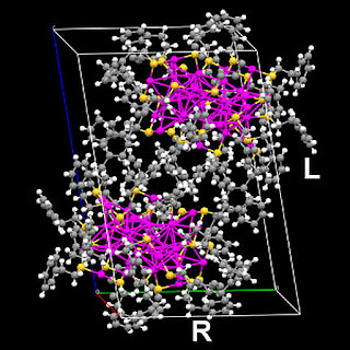
the crystal structure of a pair of gold nanoparticles that exist in a right-handed (bottom) and left-handed (top) configuration. These nanoparticles hold great promise as a chiral catalyst—a tool highly sought-after by the pharmaceutical industry.
"Growing a pure crystal from nanoparticles is very challenging, and you may not even be able to get a crystal at all," said Jin, an assistant professor of chemistry in CMU's Mellon College of Science. "In the nanoparticle community, the crystal structures of only three nanoparticles have been reported."

In Jin's case, x-ray crystallography revealed that the gold nanoparticle is chiral. Chemists typically probe the internal chiral structure of gold nanoparticles using a technique called circular dichoism spectroscopy. When pure chiral molecules are exposed to circularly polarized light, each isomer absorbs the light differently, resulting in a unique — and of opposite sign — spectrum for each isomer. The process of creating the gold nanoparticles, however, often results in a 50/50 mix of each isomer, known as racemates.

"Because the spectrum is of opposite sign for each isomer, they cancel each other out and the net optical response is zero.

This makes circular dichoism (CD) spectroscopy useless when it comes to determining the chirality of gold nanoparticles in 50/50 mixtures," said Gil, associate research professor of chemistry and director of the Department of Chemistry's NMR Facility.

Since Jin couldn't use circular dichoism spectroscopy, Gil was able to use NMR to help Jin distinguish between his gold nanoparticles' left- and right-handed isomers.

NMR spectroscopy takes advantage of the physical phenomenon wherein some nuclei wobble and spin like tops, emitting and absorbing a radio frequency signal in a magnetic field. By observing the behavior of these spinning nuclei, scientists can piece together the chemical structure of the compound.

In 1957, scientists observed that the hydrogen atoms of a freely rotating methylene (CH2) group produced two different frequencies if they were close to a chiral center. Jin's gold nanoparticles, which have a chiral core, are cushioned by several chemical groups, including freely rotating methylene groups. Gil reasoned that the nanoparticles' chiral core should induce the methylene group's two hydrogen atoms to give off different frequencies, a phenomenon known as diastereotopicity.

Gil and Jin compared the NMR signal from the hydrogen atoms in a non-chiral gold nanoparticle with the NMR signal from the hydrogen atoms in chiral gold nanoparticle. The non-chiral nanoparticle's NMR spectrum did not reveal any differences, but the chiral nanoparticle's NMR spectrum revealed two different hydrogen signals, providing a simple and efficient way of telling whether the particle is chiral or not, even for a 50/50 mixture of isomers.

"NMR is an alternative — and very efficient — method for providing useful information about how the atoms in nanoparticles form the molecular structure. Because NMR can determine chirality in some cases, it can readily be used to determine the purity of a nanoparticle mixture," Jin said.

In current work, Jin and Qian are striving to turn their 50/50 mixture of right- and left-handed isomers into a pure solution of one or the other.

###

By: Jocelyn Duffy, jhduffy@andrew.cmu.edu, 412-268-9982

Thursday, December 08, 2011

Taking advantage of graphene's outstanding strength, light weight and solubility to enhance fluids used to drill oil wells

{EAV:1bae502f1238fffe} Graphene's star is rising as a material that could become essential to efficient, environmentally sound oil production. Rice University researchers are taking advantage of graphene's outstanding strength, light weight and solubility to enhance fluids used to drill oil wells.

The Rice University lab of chemist James Tour and scientists at M-I SWACO, a Texas-based supplier of drilling fluids and subsidiary of oil-services provider Schlumberger, have produced functionalized graphene oxide to alleviate the clogging of oil-producing pores in newly drilled wells.

The patented technique took a step closer to commercialization with the publication of new research this month in the American Chemical Society journal Applied Materials and Interfaces. Graphene is a one-atom-thick sheet of carbon that won its discoverers a Nobel Prize last year.

Rice's relationship with M-I SWACO began more than two years ago when the company funded the lab's follow-up to research that produced the first graphene additives for drilling fluids known as muds. These fluids are pumped downhole as part of the process to keep drill bits clean and remove cuttings. With traditional clay-enhanced muds, differential pressure forms a layer on the wellbore called a filter cake, which both keeps the oil from flowing out and drilling fluids from invading the tiny, oil-producing pores.

When the drill bit is removed and drilling fluid displaced, the formation oil forces remnants of the filter cake out of the pores as the well begins to produce. But sometimes the clay won't budge, and the well's productivity is reduced.

flakes of functionalized graphene oxide

Microscopic, star-shaped flakes of functionalized graphene oxide plug holes in pores in a test of the material's ability to serve as a filter cake in fluids used to drill oil wells. The single-atom-thick flakes of treated carbon are pliable but among the strongest materials known. (Credit Tour Group/Rice University)
The Tour Group discovered that microscopic, pliable flakes of graphene can form a thinner, lighter filter cake. When they encounter a pore, the flakes fold in upon themselves and look something like starfish sucked into a hole. But when well pressure is relieved, the flakes are pushed back out by the oil.

All that was known two years ago. Since then, Tour and a research team led by Dmitry Kosynkin, a former Rice postdoctoral associate and now a petroleum engineer at Saudi Aramco, have been fine-tuning the materials.

They found a few issues that needed to be dealt with. First, pristine graphene is hard to disperse in water, so it is unsuitable for water-based muds. Graphene oxide (GO) turned out to be much more soluble in fresh water, but tended to coagulate in saltwater, the basis for many muds.

The solution was to "esterify" GO flakes with alcohol. "It's a simple, one-step reaction," said Tour, Rice's T.T. and W.F. Chao Chair in Chemistry as well as a professor of mechanical engineering and materials science and of computer science. "Graphene oxide functionalized with alcohol works much better because it doesn't precipitate in the presence of salts. There's nothing exotic about it."

In a series of standard American Petroleum Institute tests, the team found the best mix of functionalized GO to be a combination of large flakes and powdered GO for reinforcement. A mud with 2 percent functionalized GO formed a filter cake an average of 22 micrometers wide -- substantially smaller than the 278-micrometer cake formed by traditional muds. GO blocked pores many times smaller than the flakes' original diameter by folding.

Aside from making the filter cake much thinner, which would give a drill bit more room to turn, the Rice mud contained less than half as many suspended solids; this would also make drilling more efficient as well as more environmentally friendly. Tour and Andreas Lüttge, a Rice professor of Earth science and chemistry, reported last year that GO is reduced to graphite, the material found in pencil lead and a natural mineral, by common bacteria.

"The most exciting aspect is the ability to modify the GO nanoparticle with a variety of functionalities," said James Friedheim, corporate director of fluids research and development at M-I SWACO and a co-author of the research. "Therefore we can 'dial in' our application by picking the right organic chemistry that will suit the purpose. The trick is just choosing the right chemistry for the right purpose."

"There's still a lot to be worked out," Tour said. "We're looking at the rheological properties, the changes in viscosity under shear. In other words, we want to know how viscous this becomes as it goes through a drill head, because that also has implications for efficiency."

Muds may help graphene live up to its commercial promise, Tour said. "Everybody thinks of graphene in electronics or in composites, but this would be a use for large amounts of graphene, and it could happen soon," he said.

Friedheim agreed. "With the team we currently have assembled, Jim Tour's group and some development scientists at M-I SWACO, I am confident that we are close to both technical and commercial success."

###

Other authors of the paper are Rice graduate student Gabriel Ceriotti, former Rice research associates Kurt Wilson and Jay Lomeda, and M-I SWACO researchers Jason Scorsone and Arvind Patel.

Located on a 300-acre forested campus in Houston, Rice University is consistently ranked among the nation's top 20 universities by U.S. News & World Report. Rice has highly respected schools of Architecture, Business, Continuing Studies, Engineering, Humanities, Music, Natural Sciences and Social Sciences and is known for its "unconventional wisdom." With 3,708 undergraduates and 2,374 graduate students, Rice's undergraduate student-to-faculty ratio is less than 6-to-1. Its residential college system builds close-knit communities and lifelong friendships, just one reason why Rice has been ranked No. 1 for best quality of life multiple times by the Princeton Review and No. 4 for "best value" among private universities by Kiplinger's Personal Finance.

Contact: David Ruth druth@rice.edu 713-348-6327 Rice University

Wednesday, December 07, 2011

Designers of next-generation devices using nanowires to deliver electric currents

ALBUQUERQUE, N.M — Unexpected voltage increases of up to 25 percent in two barely separated nanowires have been observed at Sandia National Laboratories.

Designers of next-generation devices using nanowires to deliver electric currents — including telephones, handheld computers, batteries and certain solar arrays — may need to make allowances for such surprise boosts.

“People have been working on nanowires for 20 years,” says Sandia lead researcher Mike Lilly. “At first, you study such wires individually or all together, but eventually you want a systematic way of studying the integration of nanowires into nanocircuitry. That’s what’s happening now. It’s important to know how nanowires interact with each other rather than with regular wires.”

The work was reported online at DOI: 10.1038/NNANO.2011.182 (paste address into Google), and in the upcoming December 2011 issue of Nature Nanotechnology.

Though the gallium-arsenide nanowire structures used by Lilly’s team are fragile, nanowires in general have very practical characteristics — they may crack less than their bigger cousins, they’re cheaper to produce and they offer better electronic control.

For years, the best available test method required researchers to put a charged piece of material called a gate between two nanowires on a single shelf. The gate, flooded with electrons, acted as a barrier: It maintained the integrity, in effect, of the wires on either side of it by repelling any electrons attempting to escape across it. But the smallest wire separation allowed by the gate was 80 nanometers. Nanowires in future devices will be packed together much more closely, so a much smaller gap was necessary for testing.

two individually powered nanowires

Mike Lilly observes two individually powered nanowires, embedded one above the other, in a few atomic layers of Sandia-grown crystal. The unique test device already has yielded new information about nanoworld electrical flows. (Photo by Randy Montoya)

nanowires

The suitcase-like handle are the two nanowires, one above the other. The darkest areas are gallium arsenide crystal. The two lighter areas in the shape of “plus” signs are gold gates at the top and bottom of the device. (Sandia scanning electron microscope image)
The current test design has the brilliance of simplicity. What Lilly and co-workers at McGill University in Montreal envisioned was to put the nanowires one above the other, rather than side by side, by separating them with a few atomic layers of extremely pure, home-grown crystal. This allowed them to test nanowires separated vertically by only 15 nanometers — about the distance next-generation devices are expected to require. And because each wire sits on its own independent platform, each can be independently fed and controlled by electrical inputs varied by the researchers.

While applications for technical devices interest Lilly, it’s the characteristics of nanowires as a problem in one-dimensional (1-D) basic science that fascinates him.

A 1-D wire is not your common, thick-waisted, 3-D household wire, which allows current to move horizontally, vertically, and forward; nor is it your smaller, flattened micron-sized 2-D wires in typical electronic devices that allow electrons to move forward and across but not up and down. In 1-D wires, the electrons can only move in one direction: forward, like prisoners coming to lunch, one behind the other.

“In the long run, our test device will allow us to probe how 1-D conductors are different from 2-D and 3-D conductors,” Lilly said. “They are expected to be very different, but there are relatively few experimental techniques that have been used to study the 1-D ground state.”

One reason for the difference is the Coulomb force, responsible for what is termed the Coulomb “drag” effect, regardless of whether the force hastens or retards currents. Operating between wires, the force is inversely proportional to the square of the distance; that is, in ordinary microelectronics, the force is practically unnoticeable, but at nanodistances, the force is large enough that electrons in one wire can “feel” the individual electrons moving in another placed nearby.

The drag means that the first wire needs more energy because the Coulomb force creates, in effect, increased resistance. “The amount is very small,” said Lilly, “and we can’t measure it. What we can measure is the voltage of the other wire.”

There are no straightforward answers as to why the Coulomb force creates negative or positive drag, but it does. It was named for 18th century scientist Charles August Coulomb.

What’s known is that “enough electrons get knocked along that they provide positive source at one wire end, negative at the other,” Lilly said. A voltage builds up in the opposite direction to keep electrons in place,” thus increasing drag.

The so-called Fermi sea — a 3-D concept used to predict the average energy of electrons in metal — should totally break down in 1-D wires, which instead should form a Luttinger liquid, Lilly said. A Luttinger liquid is a theoretical model that describes the interactions of electrons in a 1-D conductor. To better understand the Luttinger liquid is Lilly’s underlying motive for the experiment. (Enrico Fermi was a leading theoretical physicist of the 20th century who played an important role in the development of the atomic bomb. Joaquin Luttinger was a 20th century physicist known for his theories of how electrons interact in one-dimensional metals.)

Having an interest on many levels proved useful because making the test device “took us a very long time,” he said. “It’s not impossible to do in other labs, but Sandia has crystal-growing capabilities, a microfabrication facility and support for fundamental research from DOE’s [the Department of Energy’s] Office of Basic Energy Sciences (BES). The BES core program is interested in new science and new discoveries, like the work we’re doing in trying to understand what is going on when you’re working with very small systems.”

Device fabrication was conducted under a user project at the Center for Integrated Nanotechnologies, a DOE Office of Science national user facility jointly run by Sandia and Los Alamos national laboratories. The device design and measurement were completed under the DOE Office of Science BES/Division of Materials Science and Engineering research program.

The work required the crystal-growing expertise of Sandia researcher John Reno, the fabrication and measurement skills of McGill doctoral student Dominique Laroche and elements of previous work by Sandia researcher Jerry Simmons.

Sandia National Laboratories is a multiprogram laboratory operated and managed by Sandia Corporation, a wholly owned subsidiary of Lockheed Martin Corporation, for the U.S. Department of Energy’s National Nuclear Security Administration. With main facilities in Albuquerque, N.M., and Livermore, Calif., Sandia has major R&D responsibilities in national security, energy and environmental technologies, and economic competitiveness.

Contact: neal singer nsinger@sandia.gov 505-845-7078 DOE/Sandia National Laboratories