Tuesday, August 30, 2011

Chang-Hwan Choi Mechanical Engineering Stevens Institute nanotech with multifunctional superhydrophobic properties repel water prevent corrosion

ONR Funds Dr. Chang-Hwan Choi to Study Nanoscale Wetting Dynamics of Superhydrophobic Surfaces.

This DURIP grant supports development of innovative anti-corrosion materials

With a fleet of ships and aircraft that work as hard as the sailors, pilots, and crew that operate them, the US Navy spends approximately $10-12 billion every year to fight corrosion on the hulls and bodies of these important vehicles. To support Office of Naval Research (ONR) development of hydrodynamically efficient and environmentally non-toxic anti-corrosion materials, Dr. Chang-Hwan Choi, Assistant Professor of Mechanical Engineering at Stevens Institute of Technology, researches nanotechnology with multifunctional superhydrophobic properties that repel water and prevent corrosion in robust and durable ways. Dr. Choi's work has recently been awarded a Defense University Research Instrumentation Program (DURIP) grant that backs this work.

"This award recognizes Stevens contributions to the world of multi-scale engineering in support of government defense initiatives. We are proud and honored to see the ever-growing number of faculty distinctions within the University," says Dr. Constantin Chassapis, Department Director of Mechanical Engineering and Deputy Dean for the School of Engineering and Science.

Dr. Choi's 2011 DURIP grant funds an environmental scanning electron microscope (ESEM) that will enhance his study of the functionalities of novel prototypes of nanostructured materials. The ESEM will allow his lab to study and observe the wetting dynamics of water—phenomena such as condensation and evaporation—on nano-patterned superhydrophobic surfaces.

Dr. Chang-Hwan Choi

Dr. Chang-Hwan Choi
ONR has already made long-term investments in Dr. Choi's superhydrophic surface research, including naming him to the prestigious Young Investigator Program. In 2010, he also received a DURIP grant to fund a state-of-the-art thin film deposition system. This instrumentation allows Dr. Choi to deposit layers of light metals such as aluminum, which is commonly used in naval applications, with engineered nanocharacteristics that create a water-repelling surface.

The capability of in-situ measurement of wetting dynamics via the ESEM will support many new experiment opportunities for faculty and students throughout Stevens and enable collaborations with industry and other universities for a variety of research topics in engineering, physics, chemistry, and biology.

In addition to research benefits, this instrumentation grant will also support educational initiatives through a new cross-disciplinary PhD concentration in Nanotechnology and the Nanotechnology Graduate Program.

As Director of the Nano and Microfluidics Laboratory at Stevens, Dr. Choi oversees international research collaborations to develop novel nanoscale materials with useful properties for a variety of applications in manufacturing, energy, and defense. Research projects in the lab are currently supported by the National Science Foundation, US Department of Energy, US Army, US Navy, and DARPA.

DURIP supports university research essential to the Department of Defense. It is one of several programs under the umbrella of University Research Initiatives to improve the quality of research and education in engineering and science disciplines critical to our national defense.

Learn more about related research at Stevens by visiting the Mechanical Engineering Department Web site or visit Undergraduate or Graduate Admissions to apply.

Contact Christine del Rosario Director of Academic Communications & Assessment Phone: 201.216.5561 Email: cdelrosa@stevens.edu

Sunday, August 28, 2011

Scientists probe the reactions that limit widespread deployment of fuel cell technologies

OAK RIDGE, Tenn., — A novel microscopy method at the Department of Energy's Oak Ridge National Laboratory is helping scientists probe the reactions that limit widespread deployment of fuel cell technologies.

ORNL researchers applied a technique called electrochemical strain microscopy that enables them to examine the dynamics of oxygen reduction/evolution reactions in fuel cell materials, which may reveal ways to redesign or cut the costs of the energy devices. The team's findings were published in Nature Chemistry.

"If we can find a way to understand the operation of the fuel cell on the basic elementary level and determine what will make it work in the most optimum fashion, it would create an entirely new window of opportunity for the development of better materials and devices," said co-author Amit Kumar, a research scientist at ORNL's Center for Nanophase Materials Sciences.

Although fuel cells have long been touted as a highly efficient way to convert chemical energy into electrical energy, their high cost -- in large part due to the use of platinum as a catalyst -- has constrained commercial production and consumption.

Large amounts of platinum are used to catalyze the fuel cell's key reaction -- -the oxygen-reduction reaction, which controls the efficiency and longevity of the cell. Yet exactly how and where the reaction takes place had not been probed because existing device-level electrochemical techniques are ill suited to study the reaction at the nanoscale. ORNL co-author Sergei Kalinin explains that certain methods like electron microscopy had failed to capture the dynamics of fuel cell operation because their resolution was effectively too high.

ORNL microscopy technique

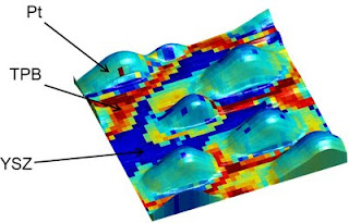
A new ORNL microscopy technique allows researchers to study key reactions in fuel cells at an unprecedented scale. The overlay shows electrochemical activity of platinum (Pt) nanoparticles on an yttria-stabilized zirconia (YSZ) surface, revealing enhanced activity along the triple-phase boundaries (TPB).
"When you want to understand how a fuel cell works, you are not interested in where single atoms are, you're interested in how they move in nanometer scale volumes," Kalinin said. "The mobile ions in these solids behave almost like a liquid. They don't stay in place. The faster these mobile ions move, the better the material is for a fuel cell application. Electrochemical strain microscopy is able to image this ion mobility."

Other electrochemical techniques are unable to study oxygen-reduction reactions because they are limited to resolutions of 10's of microns - 10,000 times larger than a nanometer.

"If the reaction is controlled by microstructure features that are much finer than a micron, let's say grain boundaries or single extended defects that are affecting the reaction, then you will never be able to catch what is giving rise to reduced or enhanced functionality of the fuel cell," said ORNL's Stephen Jesse, builder of the ESM microscope. "You would like to do this probing on a scale where you can identify each of these defects and correlate the functionality of the cell with these defects."

Although this study mainly focuses on the introduction of a technique, researchers explain their approach as a much-needed bridge between a theoretical and applied understanding of fuel cells.

"There is a huge gap between fundamental science and applied science for energy-related devices like fuel cells and batteries," Kalinin said. "The semiconducting industry, for example, is developing exponentially because the link between application and basic science is very well established. This is not the case in energy systems. They are usually much more complicated than semiconductors and therefore a lot of development is driven by trial and error type of work."

Co-authors on the study are University of Heidelberg's Francesco Ciucci and Anna Morozovska from the National Academy of Science of Ukraine, whose theoretical analysis was critical in explaining the ESM measurements.

This research was conducted at the Center for Nanophase Materials Sciences at ORNL. CNMS is one of the five DOE Nanoscale Science Research Centers supported by the DOE Office of Science, premier national user facilities for interdisciplinary research at the nanoscale. Together the NSRCs comprise a suite of complementary facilities that provide researchers with state-of-the-art capabilities to fabricate, process, characterize and model nanoscale materials, and constitute the largest infrastructure investment of the National Nanotechnology Initiative. The NSRCs are located at DOE's Argonne, Brookhaven, Lawrence Berkeley, Oak Ridge and Sandia and Los Alamos national laboratories. For more information about the DOE NSRCs, please visit science.energy.gov/nanoscale-science-research-centers/. ORNL is managed by UT-Battelle for the Department of Energy's Office of Science. ###

Thursday, August 25, 2011

Berkeley Lab researchers develop technique for dynamically controlling plasmonic airy beams

One of the earliest lessons in science that students learn is that a ray or beam of light travels in a straight line. Students also learn that light rays fan out or diffract as they travel. Recently it was discovered that light rays can travel without diffraction in a curved arc in free space. These rays of light were dubbed "Airy beams," after the English astronomer Sir George Biddell Airy, who studied what appears to be the parabolic trajectory of light in a rainbow.

Now, scientists with the Lawrence Berkeley National Laboratory (Berkeley Lab) have demonstrated the first technique that provides dynamic control in real-time of the curved trajectories of Airy beams over metallic surfaces. This development paves the way for fast-as-light, ultra-compact communication systems and optoelectronic devices,and could also stimulate revolutions in chemistry, biology and medicine.

The key to the success of this work was their ability to directly couple free-space Airy beams – using a standard tool of optics called a "grating coupler" - to quasi-particles called surface plasmon polaritons (SPPs). Directing a laser beam of light across the surface of a metal nanostructure generates electronic surface waves – called plasmons – that roll through the metal's conduction electrons (those loosely attached to molecules and atoms). The resulting interaction between plasmons and photons creates SPPs. By directly coupling Airy beams to SPPs, the researchers are able to manipulate light at an extremely small scale beyond the diffraction limit.

Plasmonic Airy Beams

Caption: Examples of the dynamic control of the plasmonic Airy beams shows switching the trajectories to different directions (a,b) and bypassing obstacles (gray solid circle in c). Left panels are numerical simulations, right panels are experimental demonstrations.

Credit: Courtesy of Xiang Zhang group. Usage Restrictions: None.

Plasmonic Airy Beams

Caption: The GIF animation shows the computer-based dynamical control of the trajectory and peak intensity position of plasmonic Airy beams achieved by Berkeley Lab’s Xiang Zhang.

Credit: courtesy of Xiang Zhang group. Usage Restrictions: None.
"Dynamic controllability of SPPs is extremely desirable for reconfigurable optical interconnections," says Xiang Zhang, the leader of this research. "We have provided a novel approach of plasmonic Airy beam to manipulate SPPs without the need of any waveguide structures over metallic surfaces, providing dynamic control of their ballistic trajectories despite any surface roughness and defects, or even getting around obstacles. This is promising not only for applications in reconfigurable optical interconnections but also for precisely manipulating particles on extremely small scales."

Zhang, a principal investigator with Berkeley Lab's Materials Sciences Division and director of the University of California at Berkeley's Nano-scale Science and Engineering Center (SINAM), is the corresponding author of a paper published in the journal Optics Letters. The paper is titled "Plasmonic Airy beams with dynamically controlled trajectories." Coauthoring the paper were Peng Zhang, Sheng Wang, Yongmin Liu, Xiaobo Yin, Changgui Lu and Zhigang Chen.

"Up to now, different plasmonic elements for manipulating surface plasmons were realized either through structuring metal surfaces or by placing dielectric structures on metals," says Peng Zhang, lead author of the Optics Letters paper and member of Xiang Zhang's research group. "Both approaches are based on the fabrication of permanent nanostructures on the metal surface, which are very difficult if not impossible to reconfigure in real time. Reconfigurability is crucial to optical interconnections, which in turn are crucial for high performance optical computing and communication systems. The reconfigurability of our technique is a huge advantage over previous approaches."

Adds co-author Zhigang Chen, a principal investigator with the Department of Physics and Astronomy at San Francisco State University, "With the reconfigurability of our plasmonic Airy beams, a small number of optical devices can be employed to perform a large number of functions within a compact system.

In addition, the unique properties of the plasmonic Airy beams open new opportunities for on-chip energy routing along arbitrary trajectories in plasmonic circuitry, and allows for dynamic manipulations of nano-particles on metal surfaces and in magneto-electronic devices."

Dynamic control of the plasmonic Airy beams is provided by a computer-controlled spatial light modulator, a device similar to a liquid crystal display that can be used to offset the incoming light waves from a laser beam with respect to a cubic phase system mask and a Fourier lens. This generates a plasmonic Airy beam on the surface of a metal whose ballistic motion can be modified.


IMAGE: The GIF animation shows the computer-based dynamical control of the trajectory and peak intensity position of plasmonic Airy beams achieved by Berkeley Lab’s Xiang Zhang.
Click here for more information.


"The direction and speed of the displacement between the incoming light and the cubic phase mask can be controlled with ease simply by displaying an animation of the shifting mask pattern as well as a shifting slit aperture in the spatial light modulator," Peng Zhang says. "Depending on the refresh rate of the spatial light modulator this can be done in real time. Furthermore, our spatial light modulator not only sets the plasmonic Airy beam into a general ballistic motion, it also enables us to control the Airy beam's peak intensity at different positions along its curved path."

The ability of the spatial light modulator to dynamically control the ballistic motions of plasmonic Airy beams without the need of any permanent guiding structures should open doors to a number of new technologies, according to Xiang and Peng Zhang and their collaborators. For example, in nano-photonics, it enables researchers to design practical reconfigurable plasmonic sensors or perform nano-particle tweezing on microchips. In biology and chemistry, it allows researchers to dynamically manipulate molecules.

Says Sheng Wang, second lead author of the Optics Letters paper, "The ultrafine nature of SPPs is extremely promising for applications of nanolithography or nanoimaging. Having dynamic tunable plasmonic Airy beams should also be useful for ultrahigh resolution bioimaging. For example, we can directly illuminate a target, for example a protein, bypassing any obstacles or reducing the background."

Adds co-author Yongmin Liu, "Our findings may inspire researchers to explore other types of non-diffracting surface waves, such as electron spin waves, in other two-dimensional systems, including graphene and topological insulators."

###

This work was supported by the U.S. Army Research Office, the U.S. Air Force Office of Scientific Research, and the National Science Foundation Nanoscale Science and Engineering Center.

Lawrence Berkeley National Laboratory addresses the world's most urgent scientific challenges by advancing sustainable energy, protecting human health, creating new materials, and revealing the origin and fate of the universe. Founded in 1931, Berkeley Lab's scientific expertise has been recognized with 12 Nobel prizes. The University of California manages Berkeley Lab for the U.S. Department of Energy's Office of Science. For more, visit

Contact: Lynn Yarris lcyarris@lbl.gov 510-486-5375 DOE/Lawrence Berkeley National Laboratory

Wednesday, August 24, 2011

Caltech researchers believe entropy can explain why water spontaneously (and unexpectedly) fills carbon nanotubes

PASADENA, Calif.—Scientists often find strange and unexpected things when they look at materials at the nanoscale—the level of single atoms and molecules. This holds true even for the most common materials, such as water.

Case in point: In the last couple of years, researchers have observed that water spontaneously flows into extremely small tubes of graphite or graphene, called carbon nanotubes. This unexpected observation is intriguing because carbon nanotubes hold promise in the emerging fields of nanofluidics and nanofiltration, where nanotubes might be able to help maintain tiny flows or separate impurities from water. However, no one has managed to explain why, at the molecular level, a stable liquid would want to confine itself to such a small area.

Now, using a novel method to calculate the dynamics of water molecules, Caltech researchers believe they have solved the mystery. It turns out that entropy, a measurement of disorder, has been the missing key.

"It's a pretty surprising result," says William Goddard, the Charles and Mary Ferkel Professor of Chemistry, Materials Science, and Applied Physics at Caltech and director of the Materials and Process Simulation Center. "People normally focus on energy in this problem, not entropy."

Increase in Disorder Leads Water to Fill Nanotubes

Caption: Caltech researchers believe entropy can explain why water spontaneously (and unexpectedly) fills carbon nanotubes. This image from the Caltech team's simulations features a cutaway of a 2.0 nanometer-diameter carbon nanotube, revealing confined water molecules.

Credit: Caltech/Tod Pascal. Usage Restrictions: None.
That's because water forms an extensive network of hydrogen bonds, which makes it very stable. Breaking those strong interactions requires energy. And since some bonds have to be broken in order for water to flow into small nanotubes, it would seem unlikely that water would do so freely.

"What we found is that it's actually a trade off," Goddard says. "You lose some of that good energy stabilization from the bonding, but in the process you gain in entropy."

Entropy is one of the driving forces that determine whether a process will occur spontaneously. It represents the number of ways a system can exist in a particular state. The more arrangements available to a system, the greater its disorder, and the higher the entropy. And in general, nature proceeds toward disorder.

When water is ideally bonded, all of the hydrogen bonds lock the molecules into place, restricting their freedom and keeping water's entropy low. What Goddard and postdoctoral scholar Tod Pascal found is that in the case of some nanotubes, water gains enough entropy by entering the tubes to outweigh the energy losses incurred by breaking some of its hydrogen bonds. Therefore, water flows spontaneously into the tubes.

Goddard and Pascal explain their findings in a paper recently published in the Proceedings of the National Academy of Sciences (PNAS). They looked at carbon nanotubes with diameters between 0.8 and 2.7 nanometers and found three different reasons why water would flow freely into the tubes, depending on diameter.

For the smallest nanotubes—those between 0.8 and 1.0 nanometers in diameter—the tubes are so minuscule that water molecules line up nearly single file within them and take on a gaslike state. That means the normal bonded structure of liquid water breaks down, giving the molecules greater freedom of motion. This increase in entropy draws water into the tubes.

At the next level, where the nanotubes have diameters between 1.1 and 1.2 nanometers, confined water molecules arrange themselves in stacked, icelike crystals. Goddard and Pascal found such nanotubes to be the perfect size—a kind of Goldilocks match—to accommodate crystallized water. These crystal-bonding interactions, not entropy, make it favorable for water to flow into the tubes.

On the largest scale studied—involving tubes whose diameters are still only 1.4 to 2.7 nanometers wide—the researchers found that the confined water molecules behave more like liquid water. However, once again, some of the normal hydrogen bonds are broken, so the molecules exhibit more freedom of motion within the tubes. And the gains in entropy more than compensate for the loss in hydrogen bonding energy.

Because the insides of the carbon nanotubes are far too small for researchers to examine experimentally, Goddard and Pascal studied the dynamics of the confined water molecules in simulations. Using a new method developed by Goddard's group with a supercomputer, they were able to calculate the entropy for the individual water molecules. In the past, such calculations have been difficult and extremely time-consuming. But the new approach, dubbed the two-phase thermodynamic model, has made the determination of entropy values relatively easy for any system.

"The old methods took eight years of computer processing time to arrive at the same entropies that we're now getting in 36 hours," Goddard says.

The team also ran simulations using an alternative description of water—one where water had its usual properties of energy, density, and viscosity, but lacked its characteristic hydrogen bonding. In that case, water did not want to flow into the nanotubes, providing additional proof that water's naturally occurring low entropy due to extensive hydrogen bonding leads to it spontaneously filling carbon nanotubes when the entropy increases.

Goddard believes that carbon nanotubes could be used to design supermolecules for water purification. By incorporating pores with the same diameters as carbon nanotubes, he thinks a polymer could be made to suck water out of solution. Such a potential application points to the need for a greater understanding of water transport through carbon nanotubes.

###

The paper, "Entropy and the driving force for the filling of carbon nanotubes with water," appeared in the July 19 issue of PNAS. Yousung Jung of the Korea Advanced Institute of Science and Technology (KAIST) also contributed to the study. Yousung completed a postdoctoral fellowship at Caltech under Nobel Prize winner Rudy Marcus before joining the faculty at KAIST, where he and Goddard are participating in the World Class University program of Korea. They are developing practical systems as part of the Energy, Environment, Water, and Sustainability Initiative, which provided the supercomputers used in this research.

Contact: Deborah Williams-Hedges debwms@caltech.edu 626-395-3227 California Institute of Technology

Monday, August 22, 2011

Key to the strength of precipitation-hardened alloys is the size, shape, and uniformity of the nanoparticles and how stable they are when heated

The nanoscale secret to stronger alloys, Scientists at Berkeley Lab find nanoparticle size is readily controlled to make stronger aluminum alloys.

Long before they knew they were doing it – as long ago as the Wright Brother's first airplane engine – metallurgists were incorporating nanoparticles in aluminum to make a strong, hard, heat-resistant alloy. The process is called solid-state precipitation, in which, after the melt has been quickly cooled, atoms of alloying metals migrate through a solid matrix and gather themselves in dispersed particles measured in billionths of a meter, only a few-score atoms wide.

Key to the strength of these precipitation-hardened alloys is the size, shape, and uniformity of the nanoparticles and how stable they are when heated. One alloy with a highly successful combination of properties is a particular formulation of aluminum, scandium, and lithium, whose precipitates are all nearly the same size. It was first made at the U.S. Department of Energy's Lawrence Berkeley National Laboratory (Berkeley Lab) in 2006 by a team led by Velimir Radmilović and Ulrich Dahmen of the Materials Sciences Division.

These scientists and their colleagues have now combined atomic-scale observations with the powerful TEAM microscope at Berkeley Lab's National Center for Electron Microscopy (NCEM) with atom-probe tomography and other experimental techniques, and with theoretical calculations, to reveal how nanoparticles consisting of cores rich in scandium and surrounded by lithium-rich shells can disperse in remarkably uniform sizes throughout a pure aluminum matrix.

Core-shell Nanoparticles

Caption: When aluminum is alloyed with the right proportions of scandium and lithium through a simple series of heat treatments, nanoparticle inclusions form in the aluminum matrix (dark background) whose cores, made of aluminum, scandium, and lithium (dark circles), vary in diameter and whose shells, made of aluminum and lithium (bright rings), vary in thickness. But their overall diameters are remarkably uniform.

Credit: Lawrence Berkeley National Laboratory. Usage Restrictions: None.

Core-shell Nanoparticle Structure

Caption: The L12 structure is shown at lower left, with aluminum atoms in gray and scandium or lithium atoms reddish green. In images of a core-shell nanoparticle made by NCEM’s TEAM microscope, each dot shows the top of a column of atoms; the kinds of atoms in each column can be calculated from the brightness and contrast of the dots. The aluminum matrix has a face-centered cubic structure in which all the atoms are aluminum, while in the L12 structure the face-centered positions are also aluminum. But in the core of the nanoparticle (upper right), the columns at the corners of the L12 unit cell are a mix of aluminum, lithium, and scandium atoms, while in the surrounding shell (lower right), the corner columns are a mix of aluminum and lithium.

Credit: Lawrence Berkeley National Laboratory. Usage Restrictions: None.
"With the TEAM microscope we were able to study the core-shell structure of these nanoprecipitates and how they form spheres that are nearly the same in diameter," says Dahmen, the director of NCEM and an author of the Nature Materials paper describing the new studies. "What's more, these particles don't change size over time, as most precipitates do. Typically, small particles get smaller and large particles get larger, a process called ripening or coarsening, which eventually weakens the alloys. But these uniform core-shell nanoprecipitates resist change."

Evolution of an alloy

In the aluminum-scandium-lithium system the researchers found that, after the initial melt, a simple two-step heating process creates first the scandium-rich cores and then the lithium-rich shells of the spherical particles. The spheres self-limit their growth to achieve the same outer dimensions, yielding a lightweight, potentially heat- and corrosion-resistant, superstrong alloy.

"Scandium is the most potent strengthener for aluminum," says NCEM's Radmilović, who is also a professor of metallurgy at the University of Belgrade, Serbia, and an author of the Nature Materials paper. "Adding less than one percent scandium can make a dramatic difference in mechanical strength, fracture resistance, corrosion resistance – all kinds of properties." Because scandium diffuses very slowly through the solid aluminum matrix, the solid mix must be heated to a high temperature (short of melting) before scandium will precipitate.

Lithium is the lightest of all metals (only hydrogen and helium are lighter) and brings not only lightness to an aluminum alloy but, potentially, strength as well. Lithium diffuses much more rapidly than scandium, at much lower temperature.

"The problem is that, by itself, lithium may not live up to its promise," says Dahmen, a long-time collaborator with Radmilović. "The trick is to convince the lithium to take on a useful crystalline structure, namely L12."

The L12 unit cell resembles a face-centered cubic cell, among the simplest and most symmetric of crystal structures. Atoms occupy each corner of an imaginary cube and are centered in the cube's six faces; in the L12 structure, the kinds of atoms at the corners may differ from those at the centers of the faces. For alloy inclusions it's one of the strongest and stablest of structures because, as Dahmen explains, "once atoms are in place in L12, it's difficult for them to move."

Dahmen credits Radmilović with the "intuition" to alloy both scandium and lithium with aluminum, heating and cooling the material in a specific series of steps. That intuition was based on Radmilović's long experience with the separate properties of aluminum-lithium and aluminum-scandium alloys and a deep understanding of how they were likely to interact. He drew up a recipe for the proportions of ingredients in the initial melt and how to cool and rewarm them.

The key to the process was to use lithium as a kind of catalyst to force a "burst of nucleation" in the scandium. After the three metals are mixed, melted, and quickly cooled or quenched, lithium serves to lower the heating needed to coax scandium to form dense core structures – although the solid mix must still be heated to 450 degrees Celsius (842 Fahrenheit) for 18 hours to form these cores, made of aluminum, lithium, and scandium. The cores average a little over nine nanometers in diameter but are not uniform in size.

Next the alloy is heated again, this time to 190˚ Celsius (374˚ F) for four hours. At the lower temperature the scandium is immobile; the freely-moving lithium forms a shell around the scandium-rich cores, much as water in a cloud crystallizes around a speck of dust to make a snowflake. The shells average about 10.5 nanometers in thickness, but their thickness is not uniform.

What's remarkable, though, is that when a core is thicker than the average, the shell is thinner than the average, and vice versa: the smaller the core, the faster the shell grows. Core size and shell size are "anticorrelated" and the result is "size focused." Whole spheres still vary somewhat, but the differences are much less than among the cores alone or the shells alone.

The structure of the cores and shells embedded in aluminum seems equally remarkable. Pure aluminum itself has a face-centered-cubic structure, and this structure is seamlessly repeated by the L12 structure of both the cores and the shells, perfectly joined with no dislocations at the interfaces between core, shell, and matrix.

Dahmen says, "It's the scandium-rich cores that convince the lithium to take on the useful L12 structure."

Joining experiment with theory

Using the TEAM microscope and a special imaging technique to look down at the tops of the regular rows of columns of atoms, the L12 structure reveals itself in groups of interlocking squares, with four columns of atoms at the corners and five columns of atoms at the lined-up centers of the faces.

In pure aluminum, all the dots are the same brightness. In the shells and cores, however, the corner columns and the face-centered columns differ in contrast – the face-centered columns are pure aluminum but the corner columns are mixed. By supplementing the high-resolution TEAM images with data from other experimental techniques it was possible to use brightness and contrast to calculate the kinds of atoms in each column.

By employing first-principles calculations, team members Colin Ophus and Mark Asta were able to model the effect of lithium on the solid-state precipitation of scandium, stimulating a sudden burst of nucleation, and also to understand why, because of the thermodynamic properties of the two metals interacting with aluminum and with each other, the precipitates are so uniform and stable.

Radmilović says, "Colin and Mark showed that lithium and scandium like each other. They also showed that by using the aluminum columns as a standard, we can calculate the intensity of the scandium and lithium by the brightness of the spot." In the shells, the corner columns contain aluminum and about 10 percent lithium. In the cores, the corner columns contain all three metals.

Dahmen says, "In recent years there has been a rapid increase in the use of 'integrative microscopy' - using a variety of techniques such as high-angular annular dark-field imaging, high-resolution phase contrast, and energy-filtered imaging and spectroscopy to attack a single problem. The TEAM microscope, which is corrected for both chromatic and spherical aberration, is unique in its ability to do all these techniques with high resolution. Understanding why nanoinclusions in aluminum-scandium-lithium are uniform is one of the best examples for the need to use integrative microscopy."

As good an alloy as aluminum-scandium-lithium is, its use may be limited by the cost of rare scandium, presently ten times the price of gold. By understanding how the alloy achieves its remarkable characteristics, the researchers fully expect that other systems with core-shell precipitates can be controlled by the same mechanisms, leading to new kinds of alloys with a range of desirable properties.

###

"Highly monodisperse core-shell particles created by solid-state reactions," by Velimir Radmilović, Colin Ophus, Emmanuelle Marquis, Marta-Dacil Rossell, Alfredo Tolley, Abhay Gautam, Mark Asta, and Ulrich Dahmen, appears in Nature Materials at www.nature.com/nmat/. Radmilović, Ophus, Rossell, Gautam, Asta, and Dahmen are presently or formerly with Berkeley Lab's Materials Sciences Division; Radmilović is also with the University of Belgrade, Marquis with the University of Michigan at Ann Arbor, Rossell with ETH Zurich, Tolley with Argentina's Comisión Nacional de Energia Atómica, and Asta with the University of California at Berkeley. This work was principally supported by DOE's Office of Science.

Lawrence Berkeley National Laboratory addresses the world's most urgent scientific challenges by advancing sustainable energy, protecting human health, creating new materials, and revealing the origin and fate of the universe. Founded in 1931, Berkeley Lab's scientific expertise has been recognized with 12 Nobel prizes. The University of California manages Berkeley Lab for the U.S. Department of Energy's Office of Science. For more, visit www.lbl.gov.

Contact: Paul Preuss paul_preuss@lbl.gov 510-486-6249 DOE/Lawrence Berkeley National Laboratory

Saturday, August 20, 2011

Newly synthesized polymer, fitted with molecular pincers of carefully tailored structure, effectively captures nicotine molecules and its analogues

Newly synthesized polymer, fitted with molecular pincers of carefully tailored structure, effectively captures nicotine molecules and its analogues. The polymer can be used for fabrication of sensitive and selective chemical sensors to determine nicotine in solutions, and in the near future also in gases. Moreover, the polymer is suitable for slow, controlled release of nicotine, e.g., for therapeutic purposes.

The collaboration of researchers of the Institute of Physical Chemistry of the Polish Academy of Sciences (IPC PAS) and of the Department of Chemistry, Wichita State University, Wichita, KS, has resulted in fabrication of a polymer trap for nicotine. Bearing molecular pincers, the polymer effectively captures nicotine molecules and its analogues, and can also release them in a controlled way. The compound will be used in reusable chemical sensors for determination of nicotine for industrial and biomedical purposes as well as in patches for smokers to evenly release nicotine to the body for a prolong time.

"The first nicotine trap has been synthesized by our US partner, Prof. Francis D'Souza, several years ago. It was a sort of molecular pincers, molecules that freely move in solution and form complexes with nicotine therein. Recently, our US-Polish team has been able to fix the pincers inside a polymer. The substance is solid, and that's why we could use it to construct chemosensors", says Prof. Włodzimierz Kutner from IPC PAS.

Polymer nicotine trap

Caption: Polymer nicotine trap is composed of a porphyrin derivative (black), in which amide pincers (green) are attached to the zinc (violet) containing macrocycle (blue). The nicotine molecule is shown in red.

Credit: IPC PAS/Tentaris/ACh. Usage Restrictions: With credit.

Polymer nicotine trap

Caption: Polymer nicotine trap is composed of a porphyrin derivative (black), in which amide pincers (green) are attached to the zinc (violet) containing macrocycle (blue). The nicotine molecule is shown in red.

Credit: IPC PAS/Tentaris/ACh. Usage Restrictions: With credit.
The core of the polymer nicotine trap, which has been recently filed for a patent, is a metalloporphyrin derivative, a substance present, i.a., in human blood. The molecule contains a ring (a macrocycle) with a centrally located zinc atom and amide pincers attached to this ring. Nicotine binds to this polymer with its two nitrogen atoms: one binds to the zinc atom, whereas the other to the pincers. "It is due to specific two-point binding that we are surer that the captured molecule is nicotine", stresses Dr. Krzysztof Noworyta from IPC PAS, adding that in one of the devised polymers the pincers are located on both sides of the zinc containing-ring plane. "Such a design clearly increases the efficiency of nicotine trapping", says Dr. Noworyta.

Beside nicotine, the polymer captures also a cotinine alkaloid produced in the metabolism of nicotine and other alkaloids often accompanying nicotine, e.g., myosmine. Polymer binding to nicotine is durable but reversible. It is the property why the new chemosensors for determination of nicotine and its analogues can be used repeatedly.

Nicotine is detected by means of a piezoelectric resonator coated by electropolymerization with a submicrometer thick polymer film. The captured nicotine increases the mass of the film resulting in a decrease in the resonant frequency of the resonator that is easy to measure.

"It can be said that we are weighing a film of our polymer all throughout the experiment. Because we know the initial polymer mass and we know that the polymer selectively captures nicotine and its analogues, an increased mass of the film means that these compounds are present in solution", explains Dr. Noworyta.

Quartz acoustic bulk wave resonators used in experiments with the new polymer allow determining nicotine in solutions. In the near future, the researchers from IPC PAS plan to establish collaboration with manufacturers of surface acoustic wave resonators. These resonators oscillate at significantly higher frequencies, thus being more sensitive, and after coating with the nicotine capturing polymer film could detect nicotine also in gases.

In the method described herein, the detection and determination of nicotine do not need to be confined to weighing. Because nicotine is electroactive, the researchers from IPC PAS are going to measure oxidation current of nicotine trapped in the polymer in parallel with the resonant frequency measurement. Simultaneous measurement with these two methods will increase the detection reliability.

The polymer with pincers for nicotine can be used, among others, in chemosensors devised to analyze nicotine content in tobacco leaves and in biomedical studies to determine nicotine metabolites in patients' body fluids. Another potential application is nicotine patches to help quit smoking. The new polymer could be used for prolong and smooth release of nicotine.

On the Polish side, the research described herein has been performed within the project "Quantum semiconductor nanostructures for applications in biology and medicine". The project, funded in 85% from the European Regional Development Fund, has been awarded to seven Polish research institutions for construction of prototype diagnostic devices on semiconductor substrates, designed for applications in biology, medicine, and environment protection as well as for the development of fundamentals of materials technologies for sensor applications and molecular diagnostics devices. Almost 50 researchers from IPC PAS participate in the project implementation.

###

The Institute of Physical Chemistry of the Polish Academy of Sciences (www.ichf.edu.pl/) was established in 1955 as one of the first chemical institutes of the PAS. The Institute's scientific profile is strongly related to the newest global trends in the development of physical chemistry and chemical physics. Scientific research is conducted in nine scientific departments. CHEMIPAN R&D Laboratories, operating as part of the Institute, implement, produce and commercialise specialist chemicals to be used, in particular, in agriculture and pharmaceutical industry. The Institute publishes approximately 200 original research papers annually.

CONTACTS:

Dr. Eng. Krzysztof Noworyta Institute of Physical Chemistry of the Polish Academy of Sciences
tel.: +48 22 3433217 e-mail: know@ichf.edu.pl

Prof. Włodzimierz Kutner Institute of Physical Chemistry of the Polish Academy of Sciences tel.: +48 22 3433217 e-mail: wkutner@ichf.edu.pl

Prof. Francis D'Souza Department of Chemistry, University of North Texas, 1155, Union Circle, #305070 Denton, TX 76203-5017 tel: (+) 940 369 8832 e-mail: francis.dsouza@unt.edu

Contact: Antoni Szafranski press@ichf.edu.pl WEB: Institute of Physical Chemistry of the Polish Academy of Sciences

Wednesday, August 17, 2011

Coating gold nanoparticles with antibodies that bind to strains of flu virus can detect influenza in minutes at a fraction of a penny per exam

Arriving at a rapid and accurate diagnosis is critical during flu outbreaks, but until now, physicians and public health officials have had to choose between a highly accurate yet time-consuming test or a rapid but error-prone test.

A new detection method developed at the University of Georgia and detailed in the August edition of the journal Analyst, however, offers the best of both worlds. By coating gold nanoparticles with antibodies that bind to specific strains of the flu virus and then measuring how the particles scatter laser light, the technology can detect influenza in minutes at a cost of only a fraction of a penny per exam.

"We've known for a long time that you can use antibodies to capture viruses and that nanoparticles have different traits based on their size," said study co-author Ralph Tripp, Georgia Research Alliance Eminent Scholar in Vaccine Development in the UGA College of Veterinary Medicine. "What we've done is combine the two to create a diagnostic test that is rapid and highly sensitive."

Working in the UGA Nanoscale Science and Engineering Center, Tripp and co-author Jeremy Driskell linked immune system proteins known as antibodies with gold nanoparticles. The gold nanoparticle-antibody complex aggregates with any virus present in a sample, and a commercially available device measures the intensity with which the solution scatters light.

Ralph Tripp

Ralph Tripp is the Georgia Research Alliance Eminent Scholar in Vaccine Development in the UGA College of Veterinary Medicine.
Driskell explained that gold nanoparticles, which are roughly a tenth of the width of a human hair, are extremely efficient at scattering light. Biological molecules such as viruses, on the other hand, are intrinsically weak light scatterers. The clustering of the virus with the gold nanoparticles causes the scattered light to fluctuate in a predictable and measurable pattern.

"The test is something that can be done literally at the point-of-care," said Driskell, who worked on the technology as an assistant research scientist in Tripp's lab. "You take your sample, put it in the instrument, hit a button and get your results."

Gold is often thought of as a costly metal, but the new diagnostic test uses such a small amount—less than what would fit on the head of the pin—that the cost is one-hundredth of a cent per test.

The researchers noted that the current standard for definitively diagnosing flu is a test known as PCR, for polymerase chain reaction. PCR can only be done in highly specialized labs and requires that specially trained personnel incubate the sample for three days, extract the DNA and then amplify it many times. The entire process, from sample collection to result, takes about a week and is too costly for routine testing.

The alternative is a rapid test known as a lateral flow assay. The test is cost effective and can be used at the point-of-care, but it can't identify the specific viral strain. It also misses up to 50 percent of infections and is especially error-prone when small quantities of virus are present, Driskell added.

By overcoming the weaknesses of existing diagnostic tests, the researchers hope to enable more timely diagnoses that can help halt the spread of flu by accurately identifying infections and allowing physicians to begin treatment early, when antiviral drugs, such as Tamiflu, are most effective.

Tripp and Driskell are planning to compare the new diagnostic test with another that Tripp and his colleagues developed that measures the change in frequency of a laser as it scatters off viral DNA or RNA. Tripp also is working to adapt the new technique so that poultry producers can rapidly detect levels of salmonella in bath water during processing. Poultry is the largest agricultural industry in Georgia, he pointed out, so the technology could have a significant impact on the state's economy.

"This test offers tremendous advantages for influenza, but we really don't want to stop there," Tripp said. "Theoretically, all we have to do is exchange our anti-influenza antibody out with an antibody for another pathogen that may be of interest, and we can do the same test for any number of infectious agents."

###

Contact: Ralph Tripp ratripp@uga.edu 706-542-1557 University of Georgia

Monday, August 15, 2011

Discovery of new magnetic data writing technique could lead to next generation computer memory

Computer files that allow us to watch videos, store pictures, and edit all kinds of media formats are nothing else but streams of "0" and "1" digital data, that is, bits and bytes. Modern computing technology is based on our ability to write, store, and retrieve digital information as efficiently as possible. In a computer hard disk, this is achieved in practice by writing information on a thin magnetic layer, where magnetic domains pointing "up" represent a "1" and magnetic domains pointing down represent a "0".

The size of these magnetic domains has now reached a few tens of nanometers, allowing us to store a Terabyte of data in the space of just about 4 square centimeters. Miniaturization, however, has created numerous problems that physicists and engineers worldwide struggle to solve at the pace demanded by an ever-growing information technology industry. The process of writing information on tiny magnetic bits one by one, as fast as possible, and with little energy consumption, represents one of the biggest hurdles in this field.

As reported this week in Nature, a team of scientists from the Catalan Institute of Nanotechnology, ICREA, and Universitat Autonoma de Barcelona, Mihai Miron, Kevin Garello, and Pietro Gambardella, in collaboration with Gilles Gaudin and colleagues working at SPINTEC in Grenoble, France, have discovered a new method to write magnetic data that fulfils all of these requirements.

Schematic of a magnetic bit fabricated by sandwiching a thin ferromagnetic Co film between Pt and AlOx layers

Schematic of a magnetic bit fabricated by sandwiching a thin ferromagnetic Co film between Pt and AlOx layers. Current pulses injected through one of the Pt strips switch the magnetization from up to dowand viceversa depending on the sign of the current.

Scanning electron micrograph of a reprogrammable magnetic switch

Figure 2: a. Scanning electron micrograph of a reprogrammable magnetic switch fabricated by placing two "bar magnets" (light blue) on top of the current injection line (light gray). The magnetic bit is shown at the center (blue). b. The polarity of the current pulses (top panel) determines the direction of the magnetization (bottom panel). The amplitude and duration of each current pulse are about 2 mA and 9 ns, respectively.
Magnetic writing is currently performed using magnetic fields produced by wires and coils, a methodology suffering severe limitations in scalability and energy efficiency. The new technique eliminates the need for cumbersome magnetic fields and provides extremely simple and reversible writing of memory elements by injecting an electric current parallel to the plane of a magnetic bit. The key to this effect lies in engineering asymmetric interfaces at the top and bottom of the magnetic layer, which induces an electric field across the material, in this case a cobalt film less than one nanometer thick sandwiched between platinum and aluminum oxide.

Due to subtle relativistic effects, electrons traversing the Co layer effectively see the material's electric field as a magnetic field, which in turn twists their magnetization. Depending on the intensity of the current and the direction of the magnetization, one can induce an effective magnetic field, intrinsic to the material that is strong enough to reverse the magnetization. The research team showed that this method works reliably at room temperature using current pulses that last less than 10 ns in magnetic bits as small as 200 x 200 square nanometers, while further miniaturization and faster switching appear easily within reach. Although there is currently no theory describing this effect, this work has many interesting applications for the magnetic recording industry, and in particular for the realization of magnetic random access memories, so-called MRAMs. By replacing standard RAMs, which need to be refreshed every few milliseconds, non-volatile MRAMs would allow instant power up of a computer and also save a substantial amount of energy.

An additional advantage of the discovery reported here is that current-induced magnetic writing is more efficient in "hard" magnetic layers than in "soft" ones.
This is somehow counterintuitive, as soft magnetic materials are by definition the easier to switch using external magnetic fields, but very practical since hard magnets can be miniaturized to nanometer dimensions without losing their magnetic properties. This would allow the information storage density to be increased without compromising the ability to write it. The results of this work have also led to three patent applications dealing with the fabrication of magnetic storage and logic devices.

###

Discovery of new magnetic data writing technique could lead to next generation computer memory
Ioan Mihai Miron1, Kevin Garello1, Gilles Gaudin2, Pierre-Jean Zermatten2, Marius V. Costache1, Stéphane Auffret2, Sebastien Bandiera2, Bernard Rodmacq2, Alain Schuhl2, and Pietro Gambardella1,3,4

1 Catalan Institute of Nanotechnology (ICN-CIN2), E-08193 Barcelona, Spain
2 SPINTEC, UMR-8191, CEA/CNRS/UJF/GINP, INAC, F-38054 Grenoble, France
3 Departament de Física, Universitat Autonoma de Barcelona (UAB), E-08193 Barcelona, Spain
4 Institució Catalana de Recerca i Estudis Avançats (ICREA), E-08010 Barcelona, Spain

DOI: 10.1038/nature10309 On-line version: was Published Sunday 31 July at 18h00 GMT Paper version: will be published in Nature on 11 August 2011.

CATALAN INSTITUTE OF NANOTECHNOLOGY (ICN)

The Catalan Institute of Nanotechnology (ICN) is a private foundation created in 2003 and forms part of CERCA, the Network of Research Centers launched by the Catalan Government as a key plank of the long-term strategy to foster the development of a knowledge-based economy. The ICN´s multicultural team of scientists, representing over 20 nationalities, aims to produce cutting-edge science and develop next-generation technologies by investigating the new properties of matter that arise from the fascinating behavior at the nanoscale.

Research is devoted on one side to the study and understanding of fundamental physical phenomena associated to state variables (electrons, spin, phonons, photons, plasmons, etc.), the investigation of new properties derived from tailored nanostructures, and the opening of new routes and fabrication processes for the conception of new nanodevices.

On the other side, researchers also explore the state of aggregation at the nanometric scale, the development of nanoproduction methods, synthesis, analysis, and manipulation of aggregates and structures of nanometric dimension, and the development of techniques for characterizing and manipulating nanostructures.

These lead to commercially relevant studies such as the functionalization of nanoparticles, the encapsulation of active agents, novel drugs and vaccines, new nanodevices and nanosensors, with applications in health, food, energy, environment, etc.

The Institute actively promotes collaboration among scientists from diverse areas of specialization (physics, chemistry, biology, engineering), and trains new generations of scientists, offering studentships, doctoral and post-doctoral positions.

More information: Institut Catala de Nanotecnologia Tel: +(34) 93 581 4408, Email: info@icn.cat, Web: www.icn.cat Communicacion Dept.: Ana de la Osa, ana.delaosa.icn@uab.es
Principal Researcher: Dr. Pietro Gambardella, ICREA Prof. and Physics Dep. Professor at Autonomous University of Barcelona (UAB), pietro.gambardella.icn@uab.es

Saturday, August 13, 2011

Nanostructure promotes growth of new blood vessels, mimics natural protein

Tissue deprived of oxygen (ischemia) is a serious health condition that can lead to damaged heart tissue following a heart attack and, in the case of peripheral arterial disease in limbs, amputation, particularly in diabetic patients.

Northwestern University researchers have developed a novel nanostructure that promotes the growth of new blood vessels and shows promise as a therapy for conditions where increased blood flow is needed to supply oxygen to tissue.

"An important goal in regenerative medicine is the ability to grow blood vessels on demand," said Samuel I. Stupp, Board of Trustees Professor of Chemistry, Materials Science and Engineering, and Medicine. "Enhancing blood flow at a given site is important where blood vessels are constricted or obstructed as well as in organ transplantation where blood is needed to feed the cells properly."

Stupp led the study that will be published the week of Aug. 1 by the Proceedings of the National Academy of Sciences (PNAS).

Stupp and his team designed an artificial structure that, like the natural protein it mimics, can trigger a cascade of complex events that promote the growth of new blood vessels. The protein the nanostructure mimics is called vascular endothelial growth factor, or VEGF.

The nanostructure, however, exhibits important advantages over VEGF: it remains in the tissue where it is needed for a longer period of time; it is easily injected as a liquid to the tissue; and, relative to the protein, it is inexpensive to produce. (VEGF was tested in human clinical trials but without good results, possibly due to it remaining in the tissue for only a few hours.)

Samuel Stupp"One of the major challenges in the field of ischemic tissue repair is sustained delivery of therapeutic agents to target tissue," said Douglas W. Losordo, M.D., a co-author of the paper and director of Northwestern's Feinberg Cardiovascular Research Institute. "Native VEGF has a very short tissue half-life, limiting its potency and requiring repeat dosing. By virtue of its engineering, this nanomaterial mimics VEGF but is capable of much longer life in the tissue, greatly enhancing its potency."

Losordo also is the Eileen M. Foell Professor of Heart Research at Northwestern's Feinberg School of Medicine and director of the Program in Cardiovascular Regenerative Medicine at Northwestern Memorial Hospital.

"We approached this as an engineering problem," said first author Matthew Webber, a doctoral student in Stupp's research group at the Institute for BioNanotechnology in Medicine (IBNAM). "To be able to design and create a small molecule that can assemble into nanostructures that function therapeutically is rewarding."

Stupp and his team created a nanostructure in the form of a fiber that displays on its surface a high density of peptides (potentially hundreds of thousands) per fiber. The peptides mimic the biological effect of VEGF, initiating the signaling process in cells that leads to blood vessel growth.

The extremely large number of active peptides results in a very potent therapeutic, and the size and stability of the nanofiber ensure the structure is retained longer in the tissue after injection.

After developing the nanostructure, Stupp and Webber teamed up with Losordo to test the nanostructures in vivo.

The researchers used an animal model of peripheral arterial disease and demonstrated the effectiveness of the nanofiber in treating the condition. In animals whose limbs were restricted to only 5 to 10 percent of normal blood flow, treatment with the nanofiber resulted in blood flow being restored to 75 to 80 percent of normal levels.

Treatment with the peptide alone did not produce the same therapeutic effect; the nanostructure was needed to display the peptides to produce results.

"Using simple chemistry, we have produced an artificial structure by design that can trigger complex events," said Stupp, who is director of IBNAM. "Our nanostructure shows the promise of a general approach to mimicking proteins for broader use in medicine and biotechnology."

The researchers next plan to investigate the protein mimic in a heart attack animal model.

###

The National Institutes of Health supported the research.

The paper is titled "Supramolecular Nanostructures that Mimic VEGF as a Strategy for Ischemic Tissue Repair." In addition to Stupp, Losordo and Webber, other authors of the paper are Jörn Tongers, Christina Newcomb and Katja-Theres Marquardt, of Northwestern University; and Johan Bauersachs, of Hannover Medical School, Hannover, Germany.

Contact: Megan Fellman is the science and engineering editor. Contact her at fellman@northwestern.edu 847-491-3115 Northwestern University

Thursday, August 11, 2011

Samuel K. Sia Columbia Engineering developed an innovative strategy for an integrated microfluidic-based diagnostic device—in effect, a lab on a chip

Columbia engineering innovative hand-held lab-on-a-chip could streamline blood testing worldwide. Successfully tested in Rwanda, mChip diagnoses infectious diseases like HIV and syphilis at patients' bedsides; new device could streamline blood testing worldwide

New York, NY — Samuel K. Sia, assistant professor of biomedical engineering at Columbia Engineering, has developed an innovative strategy for an integrated microfluidic-based diagnostic device—in effect, a lab-on-a-chip—that can perform complex laboratory assays, and do so with such simplicity that these tests can be carried out in the most remote regions of the world. In a paper published in Nature Medicine online on July 31, Sia presents the first published field results on how microfluidics—the manipulation of small amounts of fluids—and nanoparticles can be successfully leveraged to produce a functional low-cost diagnostic device in extreme resource-limited settings.

Sia and his team performed testing in Rwanda over the last four years in partnership with Columbia's Mailman School of Public Health and three local non-government organizations in Rwanda, targeting hundreds of patients. His device, known as mChip (mobile microfluidic chip), requires only a tiny finger prick of blood, effective even for a newborn, and gives—in less than 15 minutes—quantitative objective results that are not subject to user interpretation. This new technology significantly reduces the time between testing patients and treating them, providing medical workers in the field results that are much easier to read at a much lower cost. New low-cost diagnostics like the mChip could revolutionize medical care around the world.


"We have engineered a disposable credit card-sized device that can produce blood-based diagnostic results in minutes," said Sia. "The idea is to make a large class of diagnostic tests accessible to patients in any setting in the world, rather than forcing them to go to a clinic to draw blood and then wait days for their results."

Sia's lab at Columbia Engineering has developed the mChip devices in collaboration with Claros Diagnostics Inc., a venture capital-backed startup that Sia co-founded in 2004. (The company has recently been named by MIT's Technology Review as one of the 50 most innovative companies in the world.) The microchip inside the device is formed through injection molding and holds miniature forms of test tubes and chemicals; the cost of the chip is about $1 and the entire instrument about $100.

Sia hopes to use the mChip to help pregnant women in Rwanda who, while they may be suffering from AIDS and sexually transmitted diseases, cannot be diagnosed with any certainty because they live too far away from a clinic or hospital with a lab. "Diagnosis of infectious diseases is very important in the developing world," said Sia. "When you're in these villages, you may have the drugs for many STDs, but you don't know who to give treatments to, so the challenge really comes down to diagnostics." A version of the mChip that tests for prostate cancer has also been developed by Claros Diagnostics and was approved in 2010 for use in Europe.

Sia's work also focuses on developing new high-resolution tools to control the extracellular environments around cells, in order to study how they interact to form human tissues and organs. His lab uses techniques from a number of different fields, including biochemistry, molecular biology, microfabrication, microfluidics, materials chemistry, and cell and tissue biology.

###

Sia was named one of the world's top young innovators for 2010 by MIT's Technology Review for his work in biotechnology and medicine, and by NASA as one of 10 innovators in human health and sustainability. In 2008, he received a CAREER award from the National Science Foundation that included a $400,000 grant to support his other research specialty in three-dimensional tissue engineering. A recipient of the Walter H. Coulter Early Career Award in 2008, Sia participated in the National Academy of Engineering's U.S. Frontiers of Engineering symposium for the nation's brightest young engineers in 2007. He earned his B.Sc. in biochemistry from the University of Alberta, and his Ph.D. in biophysics from Harvard University, where he was also a postdoctoral fellow in chemistry and chemical biology.

The mChip project has been supported by funding from the National Institutes of Health and Wallace Coulter Foundation.

Columbia Engineering

Columbia University's Fu Foundation School of Engineering and Applied Science, founded in 1864, offers programs in nine departments to both undergraduate and graduate students. With facilities specifically designed and equipped to meet the laboratory and research needs of faculty and students, Columbia Engineering is home to NSF-NIH funded centers in genomic science, molecular nanostructures, materials science, and energy, as well as one of the world's leading programs in financial engineering. These interdisciplinary centers are leading the way in their respective fields while individual groups of engineers and scientists collaborate to solve some of society's more vexing challenges. www.engineering.columbia.edu/

Contact: Holly Evarts holly@engineering.columbia.edu 212-854-3206 Columbia University

Wednesday, August 10, 2011

Pulickel Ajayan has packed an entire lithium ion energy storage device into a single nanowire

Rice scientists build battery in a nanowire. Hybrid energy storage device is as small as it can possibly get

The world at large runs on lithium ion batteries. New research at Rice University shows that tiny worlds may soon do the same.

The Rice lab of Professor Pulickel Ajayan has packed an entire lithium ion energy storage device into a single nanowire, as reported this month in the American Chemical Society journal Nano Letters. The researchers believe their creation is as small as such devices can possibly get, and could be valuable as a rechargeable power source for new generations of nanoelectronics.

In their paper, researchers described testing two versions of their battery/supercapacitor hybrid. The first is a sandwich with nickel/tin anode, polyethylene oxide (PEO) electrolyte and polyaniline cathode layers; it was built as proof that lithium ions would move efficiently through the anode to the electrolyte and then to the supercapacitor-like cathode, which stores the ions in bulk and gives the device the ability to charge and discharge quickly.

The second packs the same capabilities into a single nanowire. The researchers built centimeter-scale arrays containing thousands of nanowire devices, each about 150 nanometers wide. A nanometer is a billionth of a meter, thousands of times smaller than a human hair.

ultrathin battery supercapacitor

An ultrathin battery/supercapacitor hybrid contains thousands of nanowires, each of which is a fully functional battery. The Rice University lab of Pulickel Ajayan developed the device. (Credit: Jeff Fitlow/Rice University)

nanoscale battery supercapacitor

A schematic shows nanoscale battery/supercapacitor devices in an array, as constructed at Rice University. The devices show promise for powering nanoscale electronics and as a research tool for understanding electrochemical phenomenon at the nanoscale. (Credit: Ajayan Lab/Rice University)
Ajayan's team has been inching toward single-nanowire devices for years. The researchers first reported the creation of three-dimensional nanobatteries last December. In that project, they encased vertical arrays of nickel-tin nanowires in PMMA, a widely used polymer best known as Plexiglas, which served as an electrolyte and insulator. They grew the nanowires via electrodeposition in an anodized alumina template atop a copper substrate. They widened the template's pores with a simple chemical etching technique that created a gap between the wires and the alumina, and then drop-coated PMMA to encase the wires in a smooth, consistent sheath. A chemical wash removed the template and left a forest of electrolyte-encased nanowires.

In that battery, the encased nickel-tin was the anode, but the cathode had to be attached on the outside.

The new process tucks the cathode inside the nanowires, said Ajayan, a professor of mechanical engineering and materials science. In this feat of nanoengineering, the researchers used PEO as the gel-like electrolyte that stores lithium ions and also serves as an electrical insulator between nanowires in an array.

After much trial and error, they settled on an easily synthesized polymer known as polyaniline (PANI) as their cathode. Drop-coating the widened alumina pores with PEO coats the insides, encases the anodes and leaves tubes at the top into which PANI cathodes could also be drop-coated. An aluminum current collector placed on top of the array completes the circuit.

"The idea here is to fabricate nanowire energy storage devices with ultrathin separation between the electrodes," said Arava Leela Mohana Reddy, a research scientist at Rice and co-author of the paper. "This affects the electrochemical behavior of the device. Our devices could be a very useful tool to probe nanoscale phenomenon."

The team's experimental batteries are about 50 microns tall -- about the diameter of a human hair and almost invisible when viewed edge-on, Reddy said. Theoretically, the nanowire energy storage devices can be as long and wide as the templates allow, which makes them scalable.

The nanowire devices show good capacity; the researchers are fine-tuning the materials to increase their ability to repeatedly charge and discharge, which now drops off after a about 20 cycles.

"There's a lot to be done to optimize the devices in terms of performance," said the paper's lead author, Sanketh Gowda, a chemical engineering graduate student at Rice. "Optimization of the polymer separator and its thickness and an exploration of different electrode systems could lead to improvements."

Rice graduate student Xiaobo Zhan is a co-author of the paper.

###

The Hartley Family Foundation, Rice University, National Institutes of Health, Army Research Office and Multidisciplinary University Research Initiative supported the research.

Contact: David Ruth druth@rice.edu 713-348-6327 Rice University

Tuesday, August 09, 2011

Bats can separate the cavalcade of echoes returning from their sonar pulses by distinguishing changes in amplitude VIDEO

PROVIDENCE, R.I. [Brown University] — In a paper published this week in Science, researchers at Brown University and from the Republic of Georgia have learned how bats can home in on a target, while nearly instantaneously taking account of and dismissing other objects in their midst. The trick lies in their neurons: Bats can separate the cavalcade of echoes returning from their sonar pulses by distinguishing changes in amplitude — the intensity of the sound — between different parts of each echo within 1.5 decibels, to decide whether the object is a target or just background clutter.

The minute change in amplitude is enough to cause a delay in the bats' neural response to an echo, letting the bat know what is clutter and what is the target. It is as if the bat is using two screens — a main screen that keeps it locked in on its target by virtue of its neural response to the echo and another, secondary screen that keeps note of surrounding objects but doesn't fixate on them.

"Everything the bat sees using sonar is based on the timing of the neural responses and nothing else," said James Simmons, professor of neuroscience at Brown and an author on the paper.

The research is important because it could help refine the maneuverability of sonar-led vehicles and improve their ability to remain fixed on a target even in dense, distracting surroundings.


Caption: Neuroscientists at Brown University have learned how bats can remain on target despite obstacles in their midst. The key lies in bats' neural response to echoes from their sonar pulses.

Credit: U.S. National Science Foundation. Usage Restrictions: None.

Bats use harmonic variation

Caption: Bats use harmonic variation to distinguish the echoes of obstacles or other background noise from the chosen target. It happens instantaneously.

Credit: Simmons Lab, Brown University. Usage Restrictions: None.
In a paper in the Proceedings of the National Academy of Sciences last year, Simmons and Mary Bates, who studied under Simmons and earned her doctorate last May, showed how bats avoid colliding with objects while flying in tight quarters. The key, they determined, is that bats tweak their sounds (chirps) and thus the echoes they receive to differentiate one broadcast/echo set from another. Building on that research, Bates and Simmons sought to determine how bats take note of objects in their sonar surroundings without being deterred by them — how bats prioritize the waves of echoes they are receiving from their broadcasts.

"The problem the bat is facing is that it's flying around in this really complicated environment. It's getting all these echoes back [from the sonar broadcasts it emits], and the echoes are all arriving at almost the same time," said Bates, lead author on the Science paper. "And they have no trouble at all dealing with that. We're trying to figure out perceptually how these bats distinguish an echo from a nearby target from all the background echoes that are arriving within a similar time window."

In a series of experiments, the researchers studied those times when the bats would encounter a "blind spot," when the echoes were so close together that the bat could not distinguish its target from the surrounding clutter. The range in which the bats can detect when one echo interferes with another is a mere 50 milliseconds, the researchers report.

Harmonics plays a major role. Bat chirps — sounds — generally have two harmonics. When a bat chirps, it waits for the corresponding echo. It makes a mental fingerprint of the emitted sound and its echo; if the broadcast/echo fingerprints match up precisely, then the bat "will process it and produce an image," Simmons said. In many cases, that image is an object it is targeting. But when the second harmonic is weaker in the echo fingerprint, the neurons' response is delayed by as few as 3 microseconds. That delay, while undetectable to humans, is enough to tell the bat that the object is present, but it is not its primary interest.

"What the bat does is it takes clutter and defocuses it, like a camera would, so the target remains highly defined and in focus," Simmons said.

###

Tengiz Zorikov from the Institute of Cybernetics in the Republic of Georgia contributed to the research. The U.S. Office of Naval Research, National Institutes of Health, and the National Science Foundation funded the work.

Contact: Richard Lewis Richard_Lewis@brown.edu 401-863-3766 Brown University

Monday, August 08, 2011

Eui-Hyeok Yang Stevens Institute of Technology, has been announced as a recipient of a Defense University Research Instrumentation Program grant 2011

Dr. Eui-Hyeok (EH) Yang, Associate Professor of Mechanical Engineering at Stevens Institute of Technology, has been announced as a recipient of a Defense University Research Instrumentation Program (DURIP) grant for 2011. This highly competitive award from the Air Force Office of Scientific Research (AFOSR) will enable the purchase of state-of-the-art equipment to support ongoing research in nanotechnology and nanoscale engineering.

"This award recognizes Stevens contributions to the world of multi-scale engineering in support of government defense initiatives. We are proud and honored to see the ever-growing number of faculty distinctions within the University," says Dr. Constantin Chassapis, Department Director of Mechanical Engineering and Deputy Dean for the School of Engineering and Science.

Dr. Yang's proposal funds the purchase of a high-resolution scanning probe microscope (SPM) capable of imaging in ambient conditions to directly support the needs of current federally funded research programs. These programs are involved in the development of a diverse range of technologies, including nanoelectronics, optoelectronics, and nanosensing devices based on low dimensional electronic materials including carbon nanotubes, graphene, and smart polymers. The ability to image nanoscale materials at extremely high resolutions is intrinsic to Dr. Yang's research at Stevens.

Dr. Eui-Hyeok (EH) YangFurther, this DURIP funding will significantly contribute to the overall capabilities of the Micro Device Laboratory (MDL), a multi-user facility directed by Dr. Yang. MDL hosts nanotechnology projects that will benefit from this SPM acquisition. The system will also serve as an important higher-education tool, promoting interdisciplinary collaborations and fostering a multidisciplinary research and education-intense environment among an increasing number of faculty, senior research personnel, and graduate and undergraduate students at Stevens.

Currently the Director of MDL as well as the Nanoelectronics and Nanomechatronics Laboratory, Dr. Yang has many years of experience in microscale and nanoscale technologies.
He has received additional grants and contracts from AFOSR, NASA, US Army ARDEC, and the National Science Foundation (NSF), including a recent NSF Major Research Instrumentation grant for a nanoimprint lithography system.

DURIP supports university research infrastructure essential to high quality Department of Defense relevant research by providing funding for research instrumentation that is necessary to carry out cutting-edge research. It is one of several programs under the umbrella of University Research Initiatives to improve the quality of defense research conducted by universities and support the education of engineers and scientists in disciplines critical to our national defense.

Learn more about Mechanical Engineering research by visiting the Department Web site

Contact: Christine del Rosario Director of Academic Communications & Assessment Phone: 201.216.5561 Email: cdelrosa@stevens.edu