Friday, July 22, 2011

Sandia Laboratories has developed a new technology with potential to dramatically alter air-cooling landscape in computing and microelectronics

Sandia’s “Cooler” technology offers fundamental breakthrough in heat transfer for microelectronics, other cooling applications.

Licensing opportunities now available

LIVERMORE, Calif. — Sandia National Laboratories has developed a new technology with the potential to dramatically alter the air-cooling landscape in computing and microelectronics, and lab officials are now seeking licensees in the electronics chip cooling field to license and commercialize the device.

The “Sandia Cooler,” also known as the “Air Bearing Heat Exchanger,” is a novel, proprietary air-cooling invention developed by Sandia researcher Jeff Koplow, who was recently selected by the National Academy of Engineering (NAE) to take part in the NAE’s 17th annual U.S. Frontiers of Engineering symposium.

Koplow said the Sandia Cooler technology, which is patent-pending, will significantly reduce the energy needed to cool the processor chips in data centers and large-scale computing environments. The yearly electricity bill paid by the information technology sector in the U.S. is currently on the order of seven billion dollars and continues to grow.

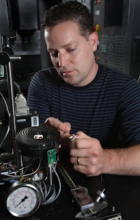
Jeff Koplow

Sandia’s Jeff Koplow makes an adjustment to an earlier prototype of his Air Bearing Heat Exchanger invention. The technology, as known as the “Sandia Cooler,” will significantly reduce the energy needed to cool the processor chips in data centers and large-scale computing environments. (Photo by Dino Vournas)
Dramatic improvements in cooling, other benefits

In a conventional CPU cooler, the heat transfer bottleneck is the boundary layer of “dead air” that clings to the cooling fins. With the Sandia Cooler, heat is efficiently transferred across a narrow air gap from a stationary base to a rotating structure. The normally stagnant boundary layer of air enveloping the cooling fins is subjected to a powerful centrifugal pumping effect, causing the boundary layer thickness to be reduced to ten times thinner than normal. This reduction enables a dramatic improvement in cooling performance within a much smaller package.

Additionally, the high speed rotation of the heat exchanger fins minimizes the problem of heat exchanger fouling. The way the redesigned cooling fins slice through the air greatly improves aerodynamic efficiency, which translates to extremely quiet operation. The Sandia Cooler’s benefits have been verified by lab researchers on a proof-of-concept prototype approximately sized to cool computer CPUs. The technology, Koplow said, also shows great potential for personal computer applications.

Broader energy sector applications

The Sandia Cooler also offers benefits in other applications where thermal management and energy efficiency are important, particularly heating, ventilation and air-conditioning (HVAC). Koplow said that if Air Bearing Heat Exchanger technology proves amenable to size scaling, it has the potential to decrease overall electrical power consumption in the U.S. by more than seven percent.

Companies interested in licensing the Sandia Cooler are invited to review and respond to the solicitation through July 15. The solicitation can be found here. Although it is first focused on licensing opportunities in the field of electronics chip cooling, Sandia will soon establish a separate process for exploring partnering and/or licensing opportunities in other fields.

A technical white paper on the Sandia Cooler technology can be found here.

Sandia’s work on the cooler technology was funded initially through internal investments. Follow-on funding is also being provided by the Department of Energy’s Office of Energy Efficiency and Renewable Energy (EERE).

Sandia National Laboratories is a multiprogram laboratory operated by Sandia Corporation, a wholly owned subsidiary of Lockheed Martin Corporation, for the U.S. Department of Energy’s National Nuclear Security Administration. With main facilities in Albuquerque, N.M., and Livermore, Calif., Sandia has major R&D responsibilities in national security, energy and environmental technologies, and economic competitiveness.

Sandia media relations contact: Mike Janes, mejanes@sandia.gov (925) 294-2447

Tuesday, July 19, 2011

The more widely and uniformly dispersed nanoscale plates of clay are in a polymer, the more fire protection the nanocomposite material provides

If materials scientists accompanied their research with theme songs, a team from the National Institute of Standards and Technology (NIST) and the University of Maryland (UMD) might be tempted to choose the garage punk song "Don't Crowd Me"* as the anthem for the promising, but still experimental nanocomposite fire retardants they are studying.

That's because the collaborators have demonstrated that the more widely and uniformly dispersed nanoscale plates of clay are in a polymer, the more fire protection the nanocomposite material provides.

Writing in the journal Polymer,** the team reports that in tests of five specimens—each with the same amount of the nanoscale filler (5 percent by weight)—the sample with the most widely dispersed clay plates was far more resistant to igniting and burning than the specimen in which the plates mostly clustered in crowds. In fact, when the two were exposed to the same amount of heat for the same length of time, the sample with the best clay dispersion degraded far more slowly. Additionally, its reduction in mass was about a third less.

In the NIST/UMD experiments, the material of interest was a polymer—a type of polystyrene, used in packaging, insulation, plastic cutlery and many other products—imbued with nanometer scale plates of montmorillonite, a type of clay with a sandwich-like molecular structure. The combination can create a material with unique properties or properties superior to those achievable by each component—clay or polymer—on its own.


Polymer-montmorillonite nanocomposites have attracted much research and commercial interest over the last decade or so. Studies have suggested that how the clay plates disperse, stack or clump in polymers dictates the properties of the resultant material. However, the evidence—especially when it comes to the flammability properties of the nanocomposites—has been somewhat muddy.

Led by NIST guest researcher Takashi Kashiwagi, the NIST-UMD team subjected their clay-dispersion-varying samples to an exhaustive battery of characterization methods and flammability tests. Affording views from the nanoscopic to the microscopic, the array of measurements and flammability tests yielded a complete picture of how the nanoscale clay plates dispersed in the polymer and how the resultant material responded when exposed to an influx of heat.

The researchers found that with better dispersion, clay plates entangle more easily when exposed to heat, thereby forming a network structure that is less likely to crack and leading to fewer gaps in the material. The result, they say, is a heat shield that slows the rate of degradation and reduces flammability. The NIST team, led by Rick Davis, is now exploring other approaches to reduce flammability, including the use of advanced materials and novel coating techniques.

* Keith Kessler, "Don't Crowd Me."
** M. Liu, X. Zhang, M. Zammarano, J.W. Gilman, R.D. Davis and T. Kashiwagi. Effect of Montmorillonite dispersion on flammability properties of poly(styrene-co-acrylonitrile) nanocomposites. Polymer. Vol. 52, Issue 14, June 22, 2011.

Contact: Mark Bello mark.bello@nist.gov 301-975-3776 National Institute of Standards and Technology (NIST)

Sunday, July 17, 2011

NIST demonstrates flexible, broadly usable technique for steadily calming vibrations of engineered mechanical objects down to the quantum ground state

BOULDER, Colo. – Showcasing new tools for widespread development of quantum circuits made of mechanical parts, scientists from the National Institute of Standards and Technology (NIST) have demonstrated a flexible, broadly usable technique for steadily calming the vibrations of an engineered mechanical object down to the quantum "ground state," the lowest possible energy level.

Described in a Nature paper posted online July 6,* the NIST experiments nearly stop the beating motion of a microscopic aluminum drum made of about 1 trillion atoms, placing the drum in a realm governed by quantum mechanics with its energy below a single quantum, or one unit of energy. Like a plucked guitar string that plays the same tone while the sound dissipates, the drum continues to beat 11 million times per second, but its range of motion approaches zero. The cooling technique and drum device together promise new machinery for quantum computing and tests of quantum theory, and could help advance the field of quantum acoustics exploring the quantum nature of mechanical vibrations.

NIST scientists used the pressure of microwave radiation, or light, to calm the motion of the drum, which is embedded in a superconducting circuit.** The circuit is designed so that the drum motion can influence the microwaves inside an electromagnetic cavity. The cooling method takes advantage of the microwave light's tendency to change frequency, if necessary, to match the frequency, or tone, at which the cavity naturally resonates.

Micro Drum Chip

Caption: Multiple versions of NIST's superconducting circuit containing a "micro drum" were fabricated on this sapphire chip, shown next to a penny for scale. NIST scientists cooled one such drum to the lowest possible energy level, the quantum ground state.

Credit: Teufel / NIST. Usage Restrictions: Please use proper credit.
"I put in the light at the wrong frequency, and it comes out at the right frequency, and it does that by stealing energy from the drum motion," says John Teufel, a NIST research affiliate who designed the drum. Teufel led the cooling experiments in NIST physicist and co-author Konrad Lehnert's lab at JILA, a joint institute of NIST and the University of Colorado Boulder.

Compared to the first engineered object to be coaxed into the quantum ground state, reported by California researchers last year, the NIST drum has a higher quality factor, so it can hold a beat longer, and it beats at a much slower rate, or lower frequency.

As a result, individual packets of energy, or quanta, can be stored 10,000 times longer (about 100 microseconds)—long enough to serve as a temporary memory for a quantum computer and a platform for exploring complex mechanical and quantum states.

In addition, the drum motion is 40 times greater per quantum, offering the possibility, for instance, of generating larger entangled "cat states"—objects that are in two places at once and also entangled, with properties that are linked even at a distance—for tests of theories such as quantum gravity. The NIST apparatus also allows researchers to measure the position of the drum directly, which is useful for force detection, with a precision closer than ever to the ultimate limit allowed by quantum mechanics.

To make engineered bulk objects obey the rules of quantum mechanics, typically observed only in atoms and smaller particles, scientists must lower an object's temperature beyond the reach of conventional refrigeration. The California researchers were able to use a passive cryogenic refrigeration technique to chill their high-frequency device enough to reach the ground state, avoiding the need for specialized techniques.

NIST's drum required the use of "sideband cooling" to reach much colder temperatures, taking advantage of strong interactions between the drum and the microwaves. This is the same idea as laser cooling of individual atoms, first demonstrated at NIST in 1978.*** Now a basic tool of atomic physics worldwide, laser cooling enabled many significant advances by allowing researchers to reduce the vibrational motion of trapped atoms to less than a single quantum. Sideband refers to a collection of light particles (photons) just above or below a specific target frequency. In the case of NIST's superconducting circuit, this stray radiation pressure, as it adjusts to the surrounding environment of the cavity, steadily removes energy from the drum motion in the same way that laser cooling slows atoms in a gas.

In the NIST experiments, the drum is first chilled in a cryogenic refrigerator using liquid helium. This lowers the drum energy to about 30 quanta. Sideband cooling then reduces the drum temperature from 20 milliKelvin (thousandths of a degree above absolute zero) to below 400 microKelvin (millionths of a degree above absolute zero), steadily lowering the drum energy to just one-third of 1 quantum.

Scientists begin the sideband cooling process by applying a drive tone to the circuit at a particular frequency below the cavity resonance. The drumbeats generate sideband photons, which naturally convert to the higher frequency of the cavity. These photons leak out of the cavity as it fills up. Each departing photon takes with it one mechanical unit of energy—one phonon—from the drum motion. At a drive intensity that corresponds to 4,000 photons in the cavity, the drum motion slows to less than 1 quantum. By detecting the scattered photons leaving the cavity, scientists can measure the mechanical motion near the lowest possible limits of uncertainty. Collectively, these steps proved that the mechanical drum entered the quantum regime.

The drum apparatus has applications in quantum computers, which could someday solve certain problems that are intractable today, even with the best supercomputers. Quantum information can be stored in the mechanical state for more than 100 microseconds before absorbing one phonon from the environment—much longer than conventional superconducting quantum bits can maintain information. The drum, thus, might serve as a short-term memory device in a superconducting quantum computer circuit, a technology under development by the same NIST research group. In addition, because mechanical oscillators can interact with light of any frequency, they could act as intermediaries for transferring quantum information between microwave and optical components.

###

Contact: Laura Ost laura.ost@nist.gov WEB: National Institute of Standards and Technology (NIST)

Saturday, July 16, 2011

Energy-storage capacity of ancient microorganism could lead to power source for synthetic cells

Energy-storage capacity of ancient microorganism could lead to power source for synthetic cells

Archaea are among the oldest known life-forms, but they are not well understood. It was only in the 1970s that these single-celled microorganisms were designated as a domain of life distinct from bacteria and multicellular organisms called eukaryotes.

Robert Gunsalus, a UCLA professor of microbiology, immunology and molecular genetics, developed an interest in Archaea because of their ability to thrive in harsh environments. Now, using state-of-the-art imaging equipment at the California NanoSystems Institute (CNSI) at UCLA, he has shown for the first time that a type of Archaea known as Methanosprillum hungatei contains incredibly efficient energy-storage structures.

The findings are published in the current issue of the journal Environmental Microbiology.

M. hungatei is of considerable environmental significance because of its unique ability to form symbiotic relationships with syntrophic bacteria to break down organic matter and produce methane gas. Yet while their important role in the food chain has been studied, little has been known about how they generate and store energy.

3-D model of M. hungatei

3-D model of M. hungatei, with granule (green)
Gunsalus has researched anaerobic organisms like M. hungatei — microbes that thrive in oxygen-depleted environments where energy is often extremely limited — for a number of years. And when Hong Zhou, a professor of microbiology, immunology and molecular genetics, arrived at UCLA in 2006, Gunsalus saw an opportunity to delve further into their mysteries.

"When Hong came to UCLA, his reputation in imaging nanoscale structures was already well established," said Gunsalus, who is also a member of the UCLA–Department of Energy Institute for Genomics and Proteomics. "His arrival on campus brought together the expertise to do what no one had yet done — a detailed study of the sub-cellular structures in M. hungatei."

Much of the actual imaging work for the study was performed by Dan Toso, a graduate student in Zhou's lab, using equipment from the Electron Imaging Center for Nanomachines (EICN), a core lab at the CNSI directed by Zhou. When Toso and the rest of the team produced the most detailed images yet made of the M. hungatei interior, they were surprised by the appearance of granules, structures measuring approximately 150 nanometers in diameter that store energy.

"Once we imaged the M. hungatei, we noticed how dark the granules appeared," said Zhou, a researcher at the CNSI. "The darkness arises from their density, and by studying this density, we discovered their energy-storage capacity."

The group was able to determine the granule density — about four times that of water — by using a Titan scanning transmission electron tomography (STEM) microscope, cryo-electron microscopy, and energy-dispersive X-ray spectroscopy, all part of the EICN lab's extensive tool set.

The tiny granules, which account for less than 0.5 percent of the cell, are so efficient that they each store 100-fold more energy than the entire rest of the cell. Each M. hungatei produces two granules, one at each end of the cell. Because all M. hungatei produce granules in the same location, and typically at the same time in their life-cycle, it is likely that their DNA contains specific genetic instructions for the creation and positioning of the granules.

The researchers hope to utilize knowledge gained from the recent sequencing of the M. hungatei genome by the U.S. Department of Energy Joint Genome Institute to further study the structures. If the specific genetic instructions for creating granules can be found in the genome, it might be possible to use the granules as a sort of chemical battery for engineered synthetic cells.

Beyond their energy-storage capacity, M. hungatei still have more secrets to reveal, according to the researchers. They also produce a distinct nanostructure sheath around their cell membrane that might serve as a sort of protection, or "cell armor," against the harsh environments in which they are typically found. Though the sheaths were discovered in the 1970s, the technology necessary for studying them in detail had yet to be developed at that time.

"M. hungatei have evolved unique features in order to survive in very harsh and low-energy environments," Gunsalus said. "The presence of cutting-edge equipment and world-class experts at UCLA allows us to closely study them, hopefully revealing their myriad of secrets."

The researchers' next goals are to elucidate the exact biological function of the granules and sheaths in M. hungatei. Many functions have been proposed for the granules, including as energy sources for cell division, or to power flagella that move the cells, or even as a protection against metal toxicity from heavy metals like iron or copper.

###

The California NanoSystems Institute at UCLA is an integrated research facility located at UCLA and UC Santa Barbara. Its mission is to foster interdisciplinary collaborations in nanoscience and nanotechnology; to train a new generation of scientists, educators and technology leaders; to generate partnerships with industry; and to contribute to the economic development and the social well-being of California, the United States and the world. The CNSI was established in 2000 with $100 million from the state of California. An additional $850 million of support has come from federal research grants and industry funding. CNSI members are drawn from UCLA's College of Letters and Science, the David Geffen School of Medicine, the School of Dentistry, the School of Public Health and the Henry Samueli School of Engineering and Applied Science. They are engaged in measuring, modifying and manipulating atoms and molecules — the building blocks of our world. Their work is carried out in an integrated laboratory environment. This dynamic research setting has enhanced understanding of phenomena at the nanoscale and promises to produce important discoveries in health, energy, the environment and information technology.

Contact: Jennifer Marcus jmarcus@cnsi.ucla.edu 310-267-4839 University of California - Los Angeles

Friday, July 15, 2011

Semiconductor nanowire laser technology that could potentially do everything from kill viruses to increase storage capacity of DVDs

University of California, Riverside engineering professor leads team that has discovered new semiconductor nanowire laser technology

RIVERSIDE, Calif. (www.ucr.edu) -- A team led by a professor at the University of California, Riverside Bourns College of Engineering has made a discovery in semiconductor nanowire laser technology that could potentially do everything from kill viruses to increase storage capacity of DVDs.

Ultraviolet semiconductor diode lasers are widely used in data processing, information storage and biology. Their applications have been limited, however, by size, cost and power. The current generation of ultraviolet lasers is based on a material called gallium nitride, but Jianlin Liu, a professor of electrical engineering, and his colleagues have made a breakthrough in zinc oxide nanowire waveguide lasers, which can offer smaller sizes, lower costs, higher powers and shorter wavelengths.

Until now, zinc oxide nanowires couldn't be used in real world light emission applications because of the lack of p-type, or positive type, material needed by all semiconductors. Liu solved that problem by doping the zinc oxide nanowires with antimony, a metalloid element, to create the p-type material.

Jianlin Liu

From left, Guoping Wang, a graduate student, Jianlin Liu, a professor of electrical engineering, and Sheng Chu, a graduate student.
The p-type zinc oxide nanowires were connected with n-type, or negative type, zinc oxide material to form a device called p-n junction diode. Powered by a battery, highly directional laser light emits only from the ends of the nanowires.

"People in the zinc oxide research community throughout the world have been trying hard to achieve this for the past decade," Liu said. "This discovery is likely to stimulate the whole field to push the technology further."

Liu's findings have been published in the July issue of Nature Nanotechnology. Co-authors are: Sheng Chu, Guoping Wang, Jieying Kong, Lin Li and Jingjian Ren, all graduate students at UC Riverside; Weihang Zhou, a student at Fudan University in China; Leonid Chernyak, a professor of physics at the University of Central Florida; Yuqing Lin, a graduate student at the University of Central Florida; and Jianze Zhao, a visiting student from Dalian University of Technology in China.

The discovery could have a wide-range of impacts.

For information storage, the zinc oxide nanowire lasers could be used to read and process much denser data on storage media such as DVDs because the ultraviolet has shorter wavelength than other lights, such as red. For example, a DVD that would store two hours of music could store four or six hours using the new type of laser.

For biology and medical therapeutics, the ultra-small laser light beam from a nanowire laser can penetrate a living cell, or excite or change its function from a bad cell to a good cell. The light could also be used to purify drinking water.

For photonics, the ultraviolet light could provide superfast data processing and transmission. Reliable small ultraviolet semiconductor diode lasers may help develop ultraviolet wireless communication technology, which is potentially better than state-of-the-art infrared communication technologies used in various electronic information systems.

While Liu and the students in his laboratory have demonstrated the p-type doping of zinc oxide and electrically powered nanowire waveguide lasing in the ultraviolet range, he said more work still needs to be done with the stability and reliability of the p-type material.

###

The work on the ZnO device was in part supported by Army Research Office Young Investigator Program and the National Science Foundation. The work on p-type ZnO was supported by the Department of Energy.

Contact: Sean Nealon sean.nealon@ucr.edu 951-827-1287 University of California - Riverside

Wednesday, July 13, 2011

Researchers developing technologies that combine laser and electric fields to manipulate fluids and tiny particles such as bacteria, , viruses and DNA

WEST LAFAYETTE, Ind. - Researchers are developing new technologies that combine a laser and electric fields to manipulate fluids and tiny particles such as bacteria, viruses and DNA for a range of potential applications, from drug manufacturing to food safety.

The technologies could bring innovative sensors and analytical devices for "lab-on-a-chip" applications, or miniature instruments that perform measurements normally requiring large laboratory equipment, said Steven T. Wereley, a Purdue University professor of mechanical engineering.

The method, called "hybrid optoelectric manipulation in microfluidics," is a potential new tool for applications including medical diagnostics, testing food and water, crime-scene forensics, and pharmaceutical manufacturing.

"This is a cutting-edge technology that has developed over the last decade from research at a handful of universities," said Aloke Kumar, a Wigner Fellow and staff member at Oak Ridge National Laboratory.

He is lead author of an article about the technology featured on the cover of the July 7 issue of Lab on a Chip magazine, published by the Royal Society of Chemistry. The article also has been flagged by the publication as a "HOT Article" and has been made free to access at blogs.rsc.org/issue-13-now-online/


This graphic illustrates a new technology that combines a laser and electric fields to manipulate fluids and tiny particles such as bacteria, viruses and DNA for a range of potential applications from drug manufacturing to food safety. The technologies could bring innovative sensors and analytical devices for "lab-on-a-chip" applications. (Stuart J. Williams, University of Louisville)
The article is written by Wereley; Kumar; Stuart J. Williams, an assistant professor of mechanical engineering at the University of Louisville; Han-Sheng Chuang, an assistant professor in the Department of Biomedical Engineering at National Cheng Kung University; and Nicolas G. Green, a researcher at the University of Southampton.

"A very important aspect is that we have achieved an integration of technologies that enables manipulation across a very wide length scale spectrum," Kumar said. "This enables us to manipulate not only big-sized objects like droplets but also tiny DNA molecules inside droplets by using one combined technique. This can greatly enhance efficiency of lab-on-a-chip sensors."

Kumar, Williams and Chuang are past Purdue doctoral students who worked with Wereley. Much of the research has been based at the Birck Nanotechnology Center at Purdue's Discovery Park.

The technologies are ready for some applications, including medical diagnostics and environmental samples, Williams said.

"There are two main thrusts in applications," he said. "The first is micro- and nanomanufacturing and the second is lab-on-a-chip sensors. The latter has demonstrated biologically relevant applications in the past couple of years, and its expansion in this field is immediate and ongoing."

The technology works by first using a red laser to position a droplet on a platform specially fabricated at Purdue. Next, a highly focused infrared laser is used to heat the droplets, and then electric fields cause the heated liquid to circulate in a "microfluidic vortex." This vortex is used to isolate specific types of particles in the circulating liquid, like a micro centrifuge. Particle concentrations replicate the size, location and shape of the infrared laser pattern.

"This works very fast," Wereley said. "It takes less than a second for particles to respond and get pulled out of solution."

Systems using the hybrid optoelectric approach can be designed to precisely detect, manipulate and screen certain types of bacteria, including particular strains that render heavy metals less toxic.

"We are shooting for biological applications, such as groundwater remediation," Wereley said. "Even within the same strain of bacteria some are good at the task and some are not, and this technology makes it possible to efficiently cull those bacteria from others. The bacteria could be injected into the contaminated ground. You seed the ground with the bacteria, but first you need to find an economical way to separate it."

Purdue researchers also are pursuing the technology for pharmaceutical manufacturing, he said.

"These types of technology are good at being very dynamic, which means you can decide in real time to grab all particles of one size or one type and put them somewhere," Wereley said. "This is important for the field of pharmacy because a number of drugs are manufactured from solid particles suspended in liquid. The particles have to be collected and separated from the liquid."

This process is now done using filters and centrifuges.

"A centrifuge does the same sort of thing but it's global, it creates a force on every particle, whereas this new technology can specifically isolate only certain particles," Wereley said. "We can, say, collect all the particles that are one micron in diameter or get rid of anything bigger than two microns, so you can dynamically select which particles you want to keep."

The technology also may be used as a tool for nanomanufacturing because it shows promise for the assembly of suspended particles, called colloids. The ability to construct objects with colloids makes it possible to create structures with particular mechanical and thermal characteristics to manufacture electronic devices and tiny mechanical parts. The nanomanufacturing applications are at least five years away, he said.

The technology also can be used to learn fundamental electrokinetic forces of molecules and biological structures, which is difficult to do with existing technologies.

"Thus there are very fundamental science applications of these technologies as well," Kumar said.

Writer: Emil Venere, 765-494-4709, venere@purdue.edu

Sources: Steven T. Wereley, 765-494-5624, wereley@purdue.edu Aloke Kumar, 865-574-8661, alokek@gmail.com, Stuart J Williams, 502-852-6340, stuart.williams@louisville.edu, Han-Sheng Chuang, 215-746-2993, hchuan@seas.upenn.edu

Note to Journalists: An electronic copy of the research paper is available from the journal or by contacting Emi Venere, Purdue News Service, at 765-494-4709, venere@purdue.edu

Tuesday, July 12, 2011

Utilising the full colour spectrum of synchrotron light, opening the way for faster 3D nanoimaging

Researchers can now see objects more precisely and faster at the nanoscale due to utilising the full colour spectrum of synchrotron light, opening the way for faster 3D nanoimaging.

This new methodology will provide for enhanced nanoimaging for studying bio samples for medical research, improved drug development and advanced materials for engineering.

Using the Advanced Photon Source, a synchrotron facility in Chicago, USA, researchers from the ARC Centre of Excellence for Coherent X-ray Science (CXS), headquartered at the University of Melbourne, Australia, revealed that by utilizing the full spectrum of colours of the synchrotron, they increased the clarity of biological samples and obtained a 60-fold increase in the speed of imaging.

Professor Keith Nugent, Laureate Professor of Physics at the University of Melbourne and Research Director of CXS, said the discovery was an exciting development.

"Typically for best imaging, researchers need to convert samples to crystals, but this is not always possible in all samples," he said.

"This discovery of utilising full colour synchrotron light to improve precision and speed of imaging has huge potential in the field," he said.

Dr Brian Abbey

Dr Brian Abbey
The international project was led by Dr Brian Abbey of the University of Melbourne's School of Physics and CXS, whose team made the discovery.

"We will now be able to see things in detail at the nanoscale much more easily. It is like going from an old film camera to the latest digital SLR.'

"The increase in speed, in particular, opens the way for us to see things faster in 3D at the nanoscale, which has previously taken an impracticably long time," Dr Abbey said.

The paper was published in the international journal Nature Photonics.

###

Contact: Rebecca Scott rebeccas@unimelb.edu.au 61-383-440-181 University of Melbourne

Thursday, July 07, 2011

Physicists say possible to create a quantum dot that is magnetic under surprising circumstances

BUFFALO, N.Y. -- At the smallest scales, magnetism may not work quite the way scientists expected, according to a recent paper in Physical Review Letters by Rafal Oszwaldowski and Igor Zutic of the University at Buffalo and Andre Petukhov of the South Dakota School of Mines and Technology.

The three physicists have proposed that it would be possible to create a quantum dot -- a kind of nanoparticle -- that is magnetic under surprising circumstances.

Magnetism is determined by a property all electrons possess: spin. Individual spins are akin to tiny bar magnets, which have north and south poles. Electrons can have an "up" or "down" spin, and a material is magnetic when most of its electrons have the same spin.

Mobile electrons can act as "magnetic messengers," using their own spin to align the spins of nearby atoms. If two mobile electrons with opposite spins are in an area, conventional wisdom says that their influences should cancel out, leaving a material without magnetic properties.

But the UB-South Dakota team has proposed that at very small scales, magnetism may be more nuanced than that. It is possible, the physicists say, to observe a peculiar form of magnetism in quantum dots whose mobile electrons have opposing spins.

Igor Zutic

Theoretical physicist Igor Zutic and colleagues hope to create a quantum dot that is magnetic.
In their Physical Review Letters article, the researchers describe a theoretical scenario involving a quantum dot that contains two free-floating, mobile electrons with opposite spins, along with manganese atoms fixed at precise locations within the quantum dot.

The quantum dot's mobile electrons act as "magnetic messengers," using their own spins to align the spins of nearby manganese atoms.

Under these circumstances, conventional thinking would predict a stalemate: Each mobile electron exerts an equal influence over spins of manganese atoms, so neither is able to "win."

Through complex calculations, however, Oszwaldowski, Zutic and Petukhov show that the quantum dot's two mobile electrons will actually influence the manganese spins differently.

That's because while one mobile electron prefers to stay in the middle of the quantum dot, the other prefers to locate further toward the edges. As a result, manganese atoms in different parts of the quantum dot receive different messages about which way to align their spins.

In the "tug-of-war" that ensues, the mobile electron that interacts more intensely with the manganese atoms "wins," aligning more spins and causing the quantum dot, as a whole, to be magnetic. (For a visual representation of this tug-of-war, see Figure 1.)

This prediction, if proven, could "completely alter the basic notions that we have about magnetic interactions," Zutic says.

"When you have two mobile electrons with opposite spins, the assumption is that there is a nice balance of up and down spins, and therefore, there is no magnetic message, or nothing that could be sent to align nearby manganese spins," he says. "But what we are saying is that it is actually a tug of war. The building blocks of magnetism are still mysterious and hold many surprises."

Scientists including UB Professor Athos Petrou, UB College of Arts and Sciences Dean Bruce McCombe and UB Vice President for Research Alexander Cartwright have demonstrated experimentally that in a quantum dot with just one mobile electron, the mobile electron will act as a magnetic messenger, robustly aligning the spins of adjacent manganese atoms.

Now, Petrou and his collaborators are interested in taking their research a step further and testing the tug-of-war prediction for two-electron quantum dots, Zutic says.

Zutic adds that learning more about magnetism is important as society continues to find novel uses for magnets, which could advance technologies including lasers, medical imaging devices and, importantly, computers.

He explains the promise of magnet- or spin-based computing technology -- called "spintronics" -- by contrasting it with conventional electronics. Modern, electronic gadgets record and read data as a blueprint of ones and zeros that are represented, in circuits, by the presence or absence of electrons. Processing information requires moving electrons, which consumes energy and produces heat.

Spintronic gadgets, in contrast, store and process data by exploiting electrons' "up" and "down" spins, which can stand for the ones and zeros devices read. Future energy-saving improvements in data processing could include devices that process information by "flipping" spin instead of shuttling electrons around.

Studying how magnetism works on a small scale is particularly important, Zutic says, because "we would like to pack more information into less space."

And, of course, unraveling the mysteries of magnetism is satisfying for other, simpler reasons.

"Magnets have been fascinating people for thousands of years," Zutic says. "Some of this fascination was not always related to how you can make a better compass or a better computer hard drive. It was just peculiar that you have materials that attract one another, and you wanted to know why."

Zutic's research on magnetism is funded by the Department of Energy, Office of Naval Research, Air Force Office of Scientific Research and the National Science Foundation.

The University at Buffalo is a premier research-intensive public university, a flagship institution in the State University of New York system and its largest and most comprehensive campus. UB's more than 28,000 students pursue their academic interests through more than 300 undergraduate, graduate and professional degree programs. Founded in 1846, the University at Buffalo is a member of the Association of American Universities.

Contact: Charlotte Hsu chsu22@buffalo.edu 716-645-4655 University at Buffalo

Monday, July 04, 2011

Nano-sized sensors that detect volatile organic compounds—harmful pollutants released from paints, cleaners, pesticides and other products

A team of researchers from the National Institute of Standards and Technology (NIST), George Mason University and the University of Maryland has made nano-sized sensors that detect volatile organic compounds—harmful pollutants released from paints, cleaners, pesticides and other products—that offer several advantages over today's commercial gas sensors, including low-power room-temperature operation and the ability to detect one or several compounds over a wide range of concentrations.

The recently published work* is proof of concept for a gas sensor made of a single nanowire and metal oxide nanoclusters chosen to react to a specific organic compound. This work is the most recent of several efforts at NIST that take advantage of the unique properties of nanowires and metal oxide elements for sensing dangerous substances.

Modern commercial gas sensors are made of thin, conductive films of metal oxides. When a volatile organic compound like benzene interacts with titanium dioxide, for example, a reaction alters the current running through the film, triggering an alarm. While thin-film sensors are effective, many must operate at temperatures of 200° C (392° F) or higher. Frequent heating can degrade the materials that make up the films and contacts, causing reliability problems. In addition, most thin-film sensors work within a narrow range: one might catch a small amount of toluene in the air, but fail to sniff out a massive release of the gas. The range of the new nanowire sensors runs from just 50 parts per billion up to 1 part per 100, or 1 percent of the air in a room.

Nanowire-based Sensors

Caption: Scanning electron microscope image of a gas sensor segment fabricated of a semiconducting nanowire of gallium nitride. The nanowire of less than 500 nanometers across is coated with nanoclusters of titanium dioxide, which alters the current in the nanowire in the presence of a volatile organic compound and ultraviolet light.

Credit: NIST. Usage Restrictions: None.
These new sensors, built using the same fabrication processes that are commonly used for silicon computer chips, operate using the same basic principle, but on a much smaller scale: the gallium nitride wires are less than 500 nanometers across and less than 10 micrometers in length. Despite their microscopic size, the nanowires and titanium dioxide nanoclusters they're coated with have a high surface-to-volume ratio that makes them exquisitely sensitive.

"The electrical current flowing through our nanosensors is in the microamps range, while traditional sensors require milliamps," explains NIST's Abhishek Motayed. "So we're sensing with a lot less power and energy. The nanosensors also offer greater reliability and smaller size. They're so small that you can put them anywhere." Ultraviolet light, rather than heat, promotes the titanium dioxide to react in the presence of a volatile organic compound.

Further, each nanowire is a defect-free single crystal, rather than the conglomeration of crystal grains in thin-film sensors, so they're less prone to degradation. In reliability tests over the last year, the nano-sized sensors have not experienced failures. While the team's current experimental sensors are tuned to detect benzene as well as the similar volatile organic compounds toluene, ethylbenzene and xylene, their goal is to build a device that includes an array of nanowires and various metal oxide nanoclusters for analyzing mixtures of compounds. They plan to collaborate with other NIST teams to combine their ultraviolet light approach with heat-induced nanowire sensing technologies.

###

The portion of this work conducted at George Mason University was funded by the National Science Foundation.

* G.S. Aluri, A. Motayed, A.V. Davydov, V.P. Oleshko, K.A. Bertness, N.A. Sanford and M.V. Rao. Highly selective GaN-nanowire/TiO2-nanocluster hybrid sensors for detection of benzene and related environment pollutants. Nanotechnology. 22 295503 doi: 10.1088/0957-4484/22/29/295503

Contact: Michael Baum michaek.baum@nist.gov 301-975-2763 National Institute of Standards and Technology (NIST)

Nanoscale testing technique for irradiated materials that provides macroscale materials-strength properties

Nuclear power is a major component of our nation's long-term clean-energy future, but the technology has come under increased scrutiny in the wake of Japan's recent Fukushima disaster. Indeed, many nations have called for checks and "stress tests" to ensure nuclear plants are operating safely.

In the United States, about 20 percent of our electricity and almost 70 percent of the electricity from emission-free sources, including renewable technologies and hydroelectric power plants, is supplied by nuclear power. Along with power generation, many of the world's nuclear facilities are used for research, materials testing, or the production of radioisotopes for the medical industry. The service life of structural and functional material components in these facilities is therefore crucial for ensuring reliable operation and safety.

Now scientists at Berkeley Lab, the University of California at Berkeley, and Los Alamos National Laboratory have devised a nanoscale testing technique for irradiated materials that provides macroscale materials-strength properties. This technique could help accelerate the development of new materials for nuclear applications and reduce the amount of material required for testing of facilities already in service.

compression tests of copper specimens irradiated with high-energy protons

Caption: Scientists at Lawrence Berkeley National Laboratory and the University of California at Berkeley conducted compression tests of copper specimens irradiated with high-energy protons, designed to model how damage from radiation affects the mechanical properties of copper. By using a specialized in situ mechanical testing device in a transmission electron microscope at the National Center for Electron Microscopy, the team could examine -- with nanoscale resolution -- the localized nature of this deformation. (Scales in nanometers, millionths of a meter.)

Credit: Minor et al, Lawrence Berkeley National Laboratory. Usage Restrictions: with credit as given.
"Nanoscale mechanical tests always give you higher strengths than the macroscale, bulk values for a material. This is a problem if you actually want use a nanoscale test to tell you something about the bulk-material properties," said Andrew Minor, a faculty scientist in the National Center for Electron Microscopy (NCEM) and an associate professor in the materials science and engineering department at UC Berkeley. "We have shown you can actually get real properties from irradiated specimens as small as 400 nanometers in diameter, which really opens up the field of nuclear materials to take advantage of nanoscale testing."

In this study, Minor and his colleagues conducted compression tests of copper specimens irradiated with high-energy protons, designed to model how damage from radiation affects the mechanical properties of copper. By using a specialized in situ mechanical testing device in a transmission electron microscope at NCEM, the team could examine — with nanoscale resolution — the nature of the deformation and how it was localized to just a few atomic planes.

Three-dimensional defects within the copper created by radiation can block the motion of one-dimensional defects in the crystal structure, called dislocations. This interaction causes irradiated materials to become brittle, and alters the amount of force a material can withstand before it eventually breaks. By translating nanoscale strength values into bulk properties, this technique could help reactor designers find suitable materials for engineering components in nuclear plants.

"This small-scale testing technique could help extend the lifetime of a nuclear reactor," said co-author Peter Hosemann, an assistant professor in the nuclear engineering department at UC Berkeley. "By using a smaller specimen, we limit any safety issues related to the handling of the test material and could potentially measure the exact properties of a material already being used in a 40-year-old nuclear facility to make sure this structure lasts well into the future."

Minor adds, "Understanding how materials fail is a fundamental mechanistic question. This proof of principle study gives us a model system from which we can now start to explore real, practical materials applicable to nuclear energy. By understanding the role of defects on the mechanical properties of nuclear reactor materials, we can design materials that are more resistant to radiation damage, leading to more advanced and safer nuclear technologies."

###

A paper reporting this research titled, "In situ nanocompression testing of irradiated copper," appears in Nature Materials and is available to subscribers online. Co-authoring the paper with Minor and Hosemann were Daniel Kiener and Stuart Maloy. Portions of this work at the National Center for Electron Microscopy were supported by DOE's Office of Science.

Lawrence Berkeley National Laboratory addresses the world's most urgent scientific challenges by advancing sustainable energy, protecting human health, creating new materials, and revealing the origin and fate of the universe. Founded in 1931, Berkeley Lab's scientific expertise has been recognized with 12 Nobel prizes. The University of California manages Berkeley Lab for the U.S. Department of Energy's Office of Science. For more, visit www.lbl.gov.

Contact: Aditi Risbud asrisbud@lbl.gov 510-486-4861 DOE/Lawrence Berkeley National Laboratory

Saturday, July 02, 2011

When semiconductor nanorods are exposed to light, they blink in a seemingly random pattern, Penn Physicists Observe “Campfire Effect”

PHILADELPHIA — When semiconductor nanorods are exposed to light, they blink in a seemingly random pattern. By clustering nanorods together, physicists at the University of Pennsylvania have shown that their combined “on” time is increased dramatically providing new insight into this mysterious blinking behavior.

The research was conducted by associate professor Marija Drndic’s group, including graduate student Siying Wang and postdoctorial fellows Claudia Querner and Tali Dadosh, all of the Department of Physics and Astronomy in Penn’s School of Arts and Sciences. They collaborated with Catherine Crouch of Swarthmore College and Dmitry Novikov of New York University’s School of Medicine.

Their research was published in the journal Nature Communications.

When provided with energy, whether in the form of light, electricity or certain chemicals, many semiconductors emit light. This principle is at work in light-emitting diodes, or LEDs, which are found in any number of consumer electronics.

At the macro scale, this electroluminescence is consistent; LED light bulbs, for example, can shine for years with a fraction of the energy used by even compact-fluorescent bulbs. But when semiconductors are shrunk down to nanometer size, instead of shining steadily, they turn “on” and “off” in an unpredictable fashion, switching between emitting light and being dark for variable lengths of time. For the decade since this was observed, many research groups around the world have sought to uncover the mechanism of this phenomenon, which is still not completely understood.

Blinking Nanorod Semiconductors

As more nanorods are added to a cluster, the cluster's "on" time dramatically increases. (Art: Robert Johnson)
“Blinking has been studied in many different nanoscale materials for over a decade, as it is surprising and intriguing, but it’s the statistics of the blinking that are so unusual,” Drndic said. “These nanorods can be ‘on’ and ‘off’ for all scales of time, from a microsecond to hours. That’s why we worked with Dmitry Novikov, who studies stochastic phenomena in physical and biological systems. These unusual Levi statistics arise when many factors compete with each other at different time scales, resulting in a rather complex behavior, with examples ranging from earthquakes to biological processes to stock market fluctuations.”

Drndic and her research team, through a combination of imaging techniques, have shown that clustering these nanorod semiconductors greatly increases their total “on” time in a kind of “campfire effect.” Adding a rod to the cluster has a multiplying effect on the “on” period of the group.

“If you put nanorods together, if each one blinks in rare short bursts, you would think the maximum ‘on’ time for the group will not be much bigger than that for one nanorod, since their bursts mostly don’t overlap,” Novikov said. “What we see are greatly prolonged ‘on’ bursts when nanorods are very close together, as if they help each other to keep shining, or ‘burning.’”

Drndic’s group demonstrated this by depositing cadmium selenide nanorods onto a substrate, shining a blue laser on them, then taking video under an optical microscope to observe the red light the nanorods then emitted. While that technique provided data on how long each cluster was “on,” the team needed to use transmission electron microscopy, or TEM, to distinguish each individual, 5-nanometer rod and measure the size of each cluster.

A set of gold gridlines allowed the researchers to label and locate individual nanorod clusters. Wang then accurately overlaid about a thousand stitched-together TEM images with the luminescence data that she took with the optical microscope. The researchers observed the “campfire effect” in clusters as small as two and as large as 110, when the cluster effectively took on macroscale properties and stopped blinking entirely.

While the exact mechanism that causes this prolonged luminescence can’t yet be pinpointed, Drndic’s team’s findings support the idea that interactions between electrons in the cluster are at the root of the effect.

“By moving from one end of a nanorod to the other, or otherwise changing position, we hypothesize that electrons in one rod can influence those in neighboring rods in ways that enhance the other rods’ ability to give off light,” Crouch said. “We hope our findings will give insight into these nanoscale interactions, as well as helping guide future work to understand blinking in single nanoparticles.”

As nanorods can be an order of magnitude smaller than a cell, but can emit a signal that can be relatively easily seen under a microscope, they have been long considered as potential biomarkers. Their inconsistent pattern of illumination, however, has limited their usefulness.

“Biologists use semiconductor nanocrystals as fluorescent labels. One significant disadvantage is that they blink,” Drndic said. “If the emission time could be extended to many minutes it makes them much more usable. With further development of the synthesis, perhaps clusters could be designed as improved labels.”

Future research will use more ordered nanorod assemblies and controlled inter-particle separations to further study the details of particle interactions.

This research was supported by the National Science Foundation.

Contact: Evan Lerner elerner@upenn.edu 215-573-6604 University of Pennsylvania

The phase behavior of confined water in the cylindrical pores of carbon nanotubes

COLLEGE PARK, MD —Water and ice may not be among the first things that come to mind when you think about single-walled carbon nanotubes (SWCNTs), but a Japan-based research team hoping to get a clearer understanding of the phase behavior of confined water in the cylindrical pores of carbon nanotubes zeroed in on confined water's properties and made some surprising discoveries.

The team, from Tokyo Metropolitan University, Nagoya University, Japan Science and Technology Agency, and National Institute of Advanced Industrial Science and Technology, describes their findings in the American Institute of Physics' Journal of Chemical Physics.

Although carbon nanotubes consist of hydrophobic (water repelling) graphene sheets, experimental studies on SWCNTs show that water can indeed be confined in open-ended carbon nanotubes.

This discovery gives us a deeper understanding of the properties of nanoconfined water within the pores of SWCNTs, which is a key to the future of nanoscience. It's anticipated that nanoconfined water within carbon nanotubes can open the door to the development of a variety of nifty new nanothings—nanofiltration systems, molecular nanovalves, molecular water pumps, nanoscale power cells, and even nanoscale ferroelectric devices.

Figure of Temperature-diameter Phase Diagram

Caption: This global temperature-diameter (T-D) phase diagram of water inside SWCNTs shows that, depending on the water content, hollow or filled ice will form. On the right, hollow- and filled-ice nanotubes can be calculated at low temperature for SWCNTs with diameters indicated with (a) and (b) in the lower portion of the phase diagram.

Credit: Yutaka Maniwa. Usage Restrictions: None.
"When materials are confined at the atomic scale they exhibit unusual properties not otherwise observed, due to the so-called 'nanoconfinement effect.' In geology, for example, nanoconfined water provides the driving force for frost heaves in soil, and also for the swelling of clay minerals," explains Yutaka Maniwa, a professor in the Department of Physics at Tokyo Metropolitan University. "We experimentally studied this type of effect for water using SWCNTs."

Water within SWCNTs in the range of 1.68 to 2.40 nanometers undergoes a wet-dry type of transition when temperature is decreased. And the team discovered that when SWCNTs are extremely narrow, the water inside forms tubule ices that are quite different from any bulk ices known so far. Strikingly, their melting point rises as the SWCNT diameter decreases—contrary to that of bulk water inside a large-diameter capillary. In fact, tubule ice occurred even at room temperature inside SWCNTs.

"We extended our studies to the larger diameter SWCNTs up to 2.40 nanometers and successfully proposed a global phase behavior of water," says Maniwa. "This phase diagram (See Figure) covers a crossover from microscopic to macroscopic regions. In the macroscopic region, a novel wet-dry transition was newly explored at low temperature."

Results such as these contribute to a greater understanding of fundamental science because nanoconfined water exists and plays a vital role everywhere on Earth—including our bodies. "Understanding the nanoconfined effect on the properties of materials is also crucial to develop new devices, such as proton-conducting membranes and nanofiltration," Maniwa notes.

Next up, the team plans to investigate the physical properties of confined water discovered so far inside SWCNTs (such as dielectricity and proton conduction). They will pursue this to obtain a better understanding of the molecular structure and transport properties in biological systems.

###

About AIP

The American Institute of Physics is an organization of 10 physical science societies, representing more than 135,000 scientists, engineers, and educators and is one of the world's largest publishers of scientific information in physics. AIP pursues innovation in electronic publishing of scholarly journals and offers full-solution publishing services for its Member Societies. AIP publishes 13 journals; two magazines, including its flagship publication Physics Today; and the AIP Conference Proceedings series.

About JCP

The Journal of Chemical Physics publishes concise and definitive reports of significant research in methods and applications of chemical physics. Innovative research in traditional areas of chemical physics such as spectroscopy, kinetics, statistical mechanics, and quantum mechanics continue to be areas of interest to readers of JCP. In addition, newer areas such as polymers, materials, surfaces/interfaces, information theory, and systems of biological relevance are of increasing importance. Routine applications of chemical physics techniques may not be appropriate for JCP. Content is published online daily, collected into four monthly online and printed issues (48 issues per year); the journal is published by the American Institute of Physics.

Contact: Charles E. Blue cblue@aip.org 301-209-3091 American Institute of Physics