Wednesday, June 29, 2011

Compact microspectrometer architecture achieves high resolution and wide bandwidth integrated lab-on-chip sensing systems

A new microspectrometer architecture that uses compact disc-shaped resonators could address the challenges of integrated lab-on-chip sensing systems that now require a large off-chip spectrometer to achieve high resolution.

Spectrometers have conventionally been expensive and bulky bench-top instruments used to detect and identify the molecules inside a sample by shining light on it and measuring different wavelengths of the emitted or absorbed light. Previous efforts toward miniaturizing spectrometers have reduced their size and cost, but these reductions have typically resulted in lower-resolution instruments.

"For spectrometers, it is better to be small and cheap than big and bulky -- provided that the optical performance targets are met," said Ali Adibi, a professor in the School of Electrical and Computer Engineering at the Georgia Institute of Technology. "We were able to achieve high resolution and wide bandwidth with a compact single-mode on-chip spectrometer through the use of an array of microdonut resonators, each with an outer radius of two microns."

The 81-channel on-chip spectrometer designed by Georgia Tech engineers achieved 0.6-nanometer resolution over a spectral range of more than 50 nanometers with a footprint less than one square millimeter. The simple instrument -- with its ultra-small footprint -- can be integrated with other devices, including sensors, optoelectronics, microelectronics and microfluidic channels for use in biological, chemical, medical and pharmaceutical applications.

Microspectrometer Micrograph

Caption: This is a micrograph of the microspectrometer developed Ali Adibi, a professor in the School of Electrical and Computer Engineering at Georgia Tech. The intstrument achieved 0.6-nanometer resolution over a spectral range of more than 50 nanometers with a footprint less than one square millimeter.

Credit: Georgia Tech/Zhixuan Xia. Usage Restrictions: None.

Microspectrometer Experimental Setup

Caption: Experimental setup used to test the 81-channel on-chip microspectrometer designed by Georgia Tech engineers led by Ali Adibi, a professor in the School of Electrical and Computer Engineering.

Credit: Georgia Tech/Zhixuan Xia. Usage Restrictions: None.
The microspectrometer architecture was described in a paper published on June 20 in the journal Optics Express. The research was supported by the Air Force Office of Scientific Research and the Defense Advanced Research Projects Agency.

"This architecture is promising because the quality-factor of the microdonut resonators is higher than that of microrings of the same size," said Richard Soref, a research scientist in the U.S. Air Force Research Laboratory at Hanscom Air Force Base who was not directly involved in the research. "Having such small resonators is also an advantage because they can be densely packed on a chip, enabling a large spectrum to be sampled."

Adibi's group is currently developing the next generation of these spectrometers, which are being designed to contain up to 1000 resonators and achieve 0.15-nanomater resolution with a spectral range of 150 nanometers and footprint of 200 micrometers squared.

Adibi, current graduate student Zhixuan Xia and research engineer Ali A. Eftekhar, and former research engineers Babak Momeni and Siva Yegnanarayanan designed and implemented the microspectrometer using CMOS-compatible fabrication processes. The key building element they used to construct the device was an array of miniaturized microdonut resonators, which were essentially microdiscs perforated in their centers. This research built on former Georgia Tech graduate student Mohammad Soltani's work to develop miniature microresonators, which was published in the Sept. 13, 2010 issue of the journal Optics Express.

The researchers adjusted the resonance wavelengths of different microdonut resonators by engineering their geometry. While the resonance was very sensitive to variations in the outer radius, fine-tuning could be achieved by adjusting the inner radius.

The microdonut resonators were carefully designed so that each of the resonators only tapped a small portion of the incoming spectrum, thus enabling measurement of the entire spectrum of desired wavelengths in real time.

A key advantage of this microspectrometer design, according to the researchers, is the ability to independently control and configure the resolution and operating bandwidth of each channel for different applications. The device can cover a wide range of wavelengths from approximately one to three micrometers. Extending this concept to the silicon nitride platform also enables spectrometers for visible light applications.

"The microspectrometer we designed may allow individuals to replace the big, bulky, high- resolution spectrometers with a large bandwidth they are currently using with an on-chip spectrometer the size of a penny," noted Adibi. "Our device has the potential to be a high-resolution, lightweight, compact, high-speed and versatile microspectrometer with a large dynamic range that can be used for many applications."

###

Current graduate students Qing Li and Maysamreza Chamanzar also contributed to this work.

This research was supported by the Defense Advanced Research Projects Agency (DARPA) (Award No. HR 0011-10-1-0075) and the Air Force Office of Scientific Research (AFOSR) (Award No. FA9550-06-01-2003). The content is solely the responsibility of the principal investigator and does not necessarily represent the official views of DARPA or AFOSR.

Contact: Abby Robinson abby@innovate.gatech.edu 404-385-3364 Georgia Institute of Technology Research News

Tuesday, June 28, 2011

Method of disguising nanoparticles as red blood cells enables them to evade body’s immune system and deliver cancer-fighting drugs straight to a tumor

Hello Nanotechnology Today Subscribers sookietex here. As twitter's @sookietex, please follow. i'm taking part in a promotion by Klout.com, [great service] and the new TNT show "Falling Skies" [great show]. i was chosen, along with other tweeters, to receive swag, an ‘Alien Invasion Survival Kit’ and to be part of the Show's Army of Influence.

The goal for our Army of Tweeters is to inspire interest and watchers for Falling Skies using Social Media. Participants are listed on the "Army of Influence Leaderboard" and whomever is at the top of board at the end of the promotion wins a walk-on role in a upcoming episode of Falling Skies.

Now Gentle Readers here’s what I would like YOU TO DO:

During the promotion, i’ll be tweeting A LOT about alien invasion, Falling Skies and the Human resistance movement known as the 2nd Mass [because of their location in Boston, Mass.] using the #fsincentivized hashtag. Please Retweet [RT] those tweets. Or if that's not your thing, please tweet this for me:

I want @Sookietex to win a walk-on role in the new TNT show #FallingSkies #fsincentivized

Just click the above link and hit ‘Tweet’!

Thank You and we return to our usual program,


Researchers at the University of California, San Diego have developed a novel method of disguising nanoparticles as red blood cells, which will enable them to evade the body's immune system and deliver cancer-fighting drugs straight to a tumor. Their research will be published next week in the online Early Edition of the Proceedings of the National Academy of Sciences.

The method involves collecting the membrane from a red blood cell and wrapping it like a powerful camouflaging cloak around a biodegradable polymer nanoparticle stuffed with a cocktail of small molecule drugs. Nanoparticles are less than 100 nanometers in size, about the same size as a virus.

"This is the first work that combines the natural cell membrane with a synthetic nanoparticle for drug delivery applications." said Liangfang Zhang, a nanoeningeering professor at the UC San Diego Jacobs School of Engineering and Moores UCSD Cancer Center. "This nanoparticle platform will have little risk of immune response".

polymeric nanoparticles

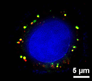
Scanning fluorescence microscopy image shows the integrity of the RBC-membrane-cloaked polymeric nanoparticles after being taken up by a cancer cell. The RBC membrane was visualized with green dye, polymeric core with red dye, and cancer cell with blue dye.
Image Credit: PNAS Early Edition

Che-Ming Hu and nanoengineering Professor Liangfang Zhang

(L-R) UCSD Ph.D. candidate in bioengineering Che-Ming Hu and nanoengineering Professor Liangfang Zhang in the lab.
Image Credit: UCSD Jacobs School of Engineering
Researchers have been working for years on developing drug delivery systems that mimic the body's natural behavior for more effective drug delivery. That means creating vehicles such as nanoparticles that can live and circulate in the body for extended periods without being attacked by the immune system. Red blood cells live in the body for up to 180 days and, as such, are "nature's long-circulation delivery vehicle," said Zhang's student Che-Ming Hu, a UCSD Ph.D. candidate in bioengineering, and first author on the paper.

Stealth nanoparticles are already used successfully in clinical cancer treatment to deliver chemotherapy drugs. They are coated in a synthetic material such as polyethylene glycol that creates a protection layer to suppress the immune system so that the nanoparticle has time to deliver its payload. Zhang said today's stealth nanoparticle drug delivery vehicles can circulate in the body for hours compared to the minutes a nanoparticle might survive without this special coating.

But in Zhang's study, nanoparticles coated in the membranes of red blood cells circulated in the bodies of lab mice for nearly two days. The study was funded through a grant from the National Institute of Health.

A shift towards personalized medicine

Using the body's own red blood cells marks a significant shift in focus and a major breakthrough in the field of personalized drug delivery research. Trying to mimic the most important properties of a red blood cell in a synthetic coating requires an in-depth biological understanding of how all the proteins and lipids function on the surface of a cell so that you know you are mimicking the right properties. Instead, Zhang's team is just taking the whole surface membrane from an actual red blood cell.

"We approached this problem from an engineering point of view and bypassed all of this fundamental biology," said Zhang. "If the red blood cell has such a feature and we know that it has something to do with the membrane -- although we don't fully understand exactly what is going on at the protein level -- we just take the whole membrane. You put the cloak on the nanoparticle, and the nanoparticle looks like a red blood cell."

Using nanoparticles to deliver drugs also reduces the hours it takes to slowly drip chemotherapy drug solutions through an intravenous line to just a few minutes for a single injection of nanoparticle drugs. This significantly improves the patient's experience and compliance with the therapeutic plan. The breakthrough could lead to more personalized drug delivery wherein a small sample of a patient's own blood could produce enough of the essential membrane to disguise the nanoparticle, reducing the risk of immune response to almost nothing.

Zhang said one of the next steps is to develop an approach for large-scale manufacturing of these biomimetic nanoparticles for clinical use, which will be done through funding from the National Science Foundation. Researchers will also add a targeting molecule to the membrane that will enable the particle to seek and bind to cancer cells, and integrate the team's technology for loading drugs into the nanoparticle core so that multiple drugs can be delivered at the same time.

Zhang said being able to deliver multiple drugs in a single nanoparticle is important because cancer cells can develop a resistance to drugs delivered individually. By combining them, and giving the nanoparticle the ability to target cancer cells, the whole cocktail can be dropped like a bomb from within the cancer cell.

###

Contact: Catherine Hockmuth chockmuth@ucsd.edu 858-822-1359 University of California - San Diego

Monday, June 27, 2011

Illuminating graphene with a mid-infrared laser could be a key to switch off conduction, thereby improving the possibilities for novel optoelectronic

College Park, MD --A team of researchers has proposed a way to turn the material graphene into a semiconductor, enabling it to control the flow of electrons with a laser "on-off switch".

Graphene is thinnest and strongest material ever discovered. It's a layer of carbon atoms only one-atom thick, but 200 times stronger than steel. It also conducts electricity extremely well and heat better than any other known material. It is almost completely transparent, yet so dense that not even atoms of helium can penetrate it. In spite of the impressive list of promising prospects, however, graphene appears to lack a critical property -- it doesn't have a "band gap."

A band gap is the basic property of semiconductors, enabling materials to control the flow of electrons. This on-off property is the foundation of computers, encoding the 0s and 1s of computer languages.

Now, a team of researchers at the National University of Córdoba and CONICET in Argentina; the Institut Catala de Nanotecnologia in Barcelona, Spain; and RWTH Aachen University, Germany; suggest that illuminating graphene with a mid-infrared laser could be a key to switch off conduction, thereby improving the possibilities for novel optoelectronic devices.

In an article featured in Applied Physics Letters, the researchers report on the first atomistic simulations of electrical conduction through a micrometer-sized graphene sample illuminated by a laser field. Their simulations show that a laser in the mid-infrared can open an observable band gap in this otherwise gapless material.

Graphene and Laser

Caption: Graphene is illuminated by a laser field (artist image). Credit: Luis E. F. Foa Torres. Usage Restrictions: None.
"Imagine that by turning on the light, graphene conduction is turned off, or vice versa. This would allow the transduction of optical into electrical signals," says Luis Foa Torres, the researcher leading this collaboration. "The problem of graphene interacting with radiation is also of current interest for the understanding of more exotic states of matter such as the topological insulators."

About AIP

The American Institute of Physics is an organization of 10 physical science societies, representing more than 135,000 scientists, engineers, and educators and is one of the world's largest publishers of scientific information in physics.

AIP pursues innovation in electronic publishing of scholarly journals and offers full-solution publishing services for its Member Societies. AIP publishes 13 journals; two magazines, including its flagship publication Physics Today; and the AIP Conference Proceedings series.

Contact: Charles E. Blue cblue@aip.org 301-209-3091 American Institute of Physics

Sunday, June 26, 2011

The world's first three-dimensional plasmon rulers, capable of measuring nanometer-scale spatial changes in macrmolecular systems VIDEO

The world's first three-dimensional plasmon rulers, capable of measuring nanometer-scale spatial changes in macrmolecular systems, have been developed by researchers with the U.S. Department of Energy (DOE)'s Lawrence Berkeley National Laboratory (Berkeley Lab), in collaboration with researchers at the University of Stuttgart, Germany. These 3D plasmon rulers could provide scientists with unprecedented details on such critical dynamic events in biology as the interaction of DNA with enzymes, the folding of proteins, the motion of peptides or the vibrations of cell membranes.

"We've demonstrated a 3D plasmon ruler, based on coupled plasmonic oligomers in combination with high-resolution plasmon spectroscopy, that enables us to retrieve the complete spatial configuration of complex macromolecular and biological processes, and to track the dynamic evolution of these processes," says Paul Alivisatos, director of Berkeley Lab and leader of this research.

Alivisatos, who is also the Larry and Diane Bock Professor of Nanotechnology at the University of California (UC), Berkeley, is the senior author of a paper in the journal Science describing this research. The paper is titled "Three-Dimensional Plasmon Rulers." Co-authoring this paper were Laura Na Liu, who at the time the work was done was a member of Alivisatos' research group but is now with Rice University, and Mario Hentschel, Thomas Weiss and Harald Giessen with the University of Stuttgart.


Caption: In this animation of a 3-D plasmon ruler, developed by a collaboration of researchers with the Lawrence Berkeley National Laboratory and the University of Stuttgart, the plasmonic assembly acts as a transducer to deliver optical information about the structural dynamics of an attached protein.

Credit: The video is courtesy of Berkeley Lab. Usage Restrictions: credit to the Paul Alivisatos research group, Lawrence Berkeley National Laboratory.

3-D Plasmon Ruler Graphic

Caption: The 3-D plasmon ruler is constructed from five gold nanorods in which one nanorod (red) is placed perpendicular between two pairs of parallel nanorods (yellow and green).

Credit: courtesy of Paul Alivisatos research group, Berkeley, CA. Usage Restrictions: None.
The nanometer scale is where the biological and materials sciences converge. As human machines and devices shrink to the size of biomolecules, scientists need tools by which to precisely measure minute structural changes and distances. To this end, researchers have been developing linear rulers based on the electronic surface waves known as "plasmons," which are generated when light travels through the confined dimensions of noble metal nanoparticles or structures, such as gold or silver.

"Two noble metallic nanoparticles in close proximity will couple with each other through their plasmon resonances to generate a light-scattering spectrum that depends strongly on the distance between the two nanoparticles," Alivisatos says. "This light-scattering effect has been used to create linear plasmon rulers that have been used to measure nanoscale distances in biological cells."

Compared to other types of molecular rulers, which are based on chemical dyes and fluorescence resonance energy transfer (FRET), plasmon rulers neither blink nor photobleach, and also offer exceptional photostability and brightness. However, until now plasmon rulers could only be used to measure distances along one dimension, a limitation that hampers any comprehensive understanding of all the biological and other soft-matter processes that take place in 3D.

"Plasmonic coupling in multiple nanoparticles placed in proximity to each other leads to light scattering spectra that are sensitive to a complete set of 3D motions," says Laura Na Liu, corresponding author of the Science paper. "The key to our success is that we were able to create sharp spectral features in the otherwise broad resonance profile of plasmon-coupled nanostructures by using interactions between quadrupolar and dipolar modes."

Liu explains that typical dipolar plasmon resonances are broad because of radiative damping. As a result, the simple coupling between multiple particles produces indistinct spectra that are not readily converted into distances.

She and her co-authors overcame this problem with a 3D ruler constructed from five gold nanorods of individually controlled length and orientation, in which one nanorod is placed perpendicular between two pairs of parallel rod nanorods to form a structure that resembles the letter H.

"The strong coupling between the single nanorod and the two parallel nanorod pairs suppresses radiative damping and allows for the excitation of two sharp quadrupolar resonances that enable high-resolution plasmon spectroscopy," Liu says. "Any conformational change in this 3D plasmonic structure will produce readily observable changes in the optical spectra."

Not only did conformational changes in their 3D plasmon rulers alter light scattering wavelengths, but the degrees of spatial freedom afforded its five nanorod structure also enabled Liu and her colleagues to distinguish the direction as well as the magnitude of structural changes.

"As a proof of concept, we fabricated a series of samples using high-precision electron beam lithography and layer-by-layer stacking nanotechniques, then embedded them with our 3D plasmon rulers in a dielectric medium on a glass substrate," Liu says. "Experimental results were in excellent agreement with the calculated spectra."

Alivisatos, Liu and their Stuttgart collaborators envision a future in which 3D plasmon rulers would, through biochemical linkers, be attached to a sample macromolecule, for example, to various points along a strand of DNA or RNA, or at different positions on a protein or peptide. The sample macromolecule would then be exposed to light and the optical responses of the 3D plasmon rulers would be measured via dark field microspectroscopy.

"The realization of 3D plasmon rulers using nanoparticles and biochemical linkers is challenging, but 3D nanoparticle assemblies with desired symmetries and configurations have been already been demonstrated," Liu says. "We believe these exciting experimental achievements along with the introduction of our new concept will pave the road toward the realization of 3D plasmon rulers in biological and other soft-matter systems."

###

This research was supported by grants from the National Institutes of Health Plasmon Rulers Project and the German Ministry of Science.

Lawrence Berkeley National Laboratory addresses the world's most urgent scientific challenges by advancing sustainable energy, protecting human health, creating new materials, and revealing the origin and fate of the universe. Founded in 1931, Berkeley Lab's scientific expertise has been recognized with 12 Nobel prizes. The University of California manages Berkeley Lab for the U.S. Department of Energy's Office of Science. For more, visit www.lbl.gov.

Contact: Lynn Yarris lcyarris@lbl.gov 510-486-5375 DOE/Lawrence Berkeley National Laboratory

Friday, June 24, 2011

Smart film that not only can be used to turn bacterial adhesion on and off, but also may be used for detecting bacteria

Rigoberto Advincula honored with 3 fellowships for polymer, nanomaterials advances.

HOUSTON, June 15, 2011 – A University of Houston (UH) chemist who is developing materials for detecting and repelling E. coli has published papers in two high-impact journals this month.

Rigoberto "Gobet" Advincula, a polymer chemist, says he and his colleagues have developed two different materials that are both equally effective against E. coli. He discusses the findings in the June issues of Chemical Communications (ChemComm) and Chemistry of Materials.

The ChemComm paper, Advincula says, describes a graphene material that is proving to be an effective antimicrobial, while the research appearing in the journal Chemistry of Materials uses a conducting polymer that can repel E. coli. He says his team has created a smart film that not only can be used to turn bacterial adhesion on and off, but also may be used for detecting bacteria. The work was done in collaboration with Debora Rodrigues and her group from UH's department of civil and environmental engineering.

Prolific in inventing new and smart materials such as these, Advincula has compiled an impressive record as a leading polymer, thin films and nanomaterials researcher. In addition to these most recent publications, three other papers were cover stories in top journals in April. In May, he released a new book with Wolfgang Knoll of the Austrian Institute of Technology titled "Functional Polymer Films" that Advincula considers to be akin to an encyclopedia on polymer thin films.

Gobet Advincula

Caption: Gobet Advincula, who is developing materials for detecting and repelling E. coli, was recently honored as a “triple fellow” with the American Chemical Society.

Credit: Thomas Campbell. Usage Restrictions: None
Additionally, Advincula was recently inducted as a fellow of the American Chemical Society (ACS), as well as being named a fellow in two of its technical divisions – the Polymer Chemistry Division and the Polymer Materials Science and Engineering Division. The ACS is the world's largest scientific society and one of the world's leading sources of authoritative scientific information. Achieving fellow status is a competitive process, based on research, contribution and service accomplishments to science and society.

"It is a rare distinction to become a triple fellow with the ACS, which has more than 163,000 members," Advincula said. "With only one out of every 1,000 members qualifying for selection as a fellow, I am extremely honored to achieve this trifecta for my work in advancing polymer and nanomaterial research and applications."

He asserts that much of this is really a tribute to his research group at UH, saying that his discovery-driven laboratory provides an environment that allows for readily filing patents, authoring publications and mentoring future scholars and inventors. He says the joy of working with students and budding scientists and engineers is reflected in his record of mentoring, with nearly 20 Ph.D. students, 50 undergraduates and dozens of high school students coming through his lab over the years.

"It is an extraordinary achievement to be named a fellow of the ACS and two ACS divisions," said David Hoffman, professor and chair of the chemistry department in the College of Natural Sciences and Mathematics at UH. "The honors are a reflection of the respect Gobet's colleagues have for him personally and for his scientific work."

In addition to his lab research, Advincula has been active in ACS, giving hundreds of presentations, organizing symposia and serving on the editorial advisory board of several scientific journals. He has nine U.S. patents and has authored more than 300 papers. Advincula, who is both a professor of chemistry and chemical engineering, has been continuously funded by the National Science Foundation, Robert A. Welch Foundation and several companies interested in the applications of his work.

###

About the University of Houston

The University of Houston is a Carnegie-designated Tier One public research university recognized by The Princeton Review as one of the nation's best colleges for undergraduate education. UH serves the globally competitive Houston and Gulf Coast Region by providing world-class faculty, experiential learning and strategic industry partnerships. Located in the nation's fourth-largest city, UH serves more than 38,500 students in the most ethnically and culturally diverse region in the country.

About the College of Natural Sciences and Mathematics

The UH College of Natural Sciences and Mathematics, with 181 ranked faculty and approximately 4,500 students, offers bachelor's, master's and doctoral degrees in the natural sciences, computational sciences and mathematics. Faculty members in the departments of biology and biochemistry, chemistry, computer science, earth and atmospheric sciences, mathematics and physics conduct internationally recognized research in collaboration with industry, Texas Medical Center institutions, NASA and others worldwide.

Contact: Lisa Merkl lkmerkl@uh.edu 713-743-8192 University of Houston

Thursday, June 23, 2011

Polaritons have increased coupling strength when confined to nanoscale semiconductors

PHILADELPHIA—New engineering research at the University of Pennsylvania demonstrates that polaritons have increased coupling strength when confined to nanoscale semiconductors. This represents a promising advance in the field of photonics: smaller and faster circuits that use light rather than electricity.

The research was conducted by assistant professor Ritesh Agarwal, postdoctoral fellow Lambert van Vugt and graduate student Brian Piccione of the Department of Materials Science and Engineering in Penn’s School of Engineering and Applied Science. Chang-Hee Cho and Pavan Nukala, also of the Materials Science department, contributed to the study.

Their work was published in the journal Proceedings of the National Academy of Sciences.

Polaritons are quasiparticles, combinations of physical particles and the energy they contribute to a system that can be measured and tracked as a single unit. Polaritons are combinations of photons and another quasiparticle, excitons. Together, they have qualities of both light and electric charge, without being fully either.

“An exciton is a combination of a an electron, which has negative charge and an electron hole, which has a positive charge. Light is an oscillating electro-magnetic field, so it can couple with the excitons,” Agarwal said. “When their frequencies match, they can talk to one another; both of their oscillations become more pronounced.”

computer simulation of a one-dimensional cavity wave in a 200nm nanowire

A computer simulation of a one-dimensional cavity wave in a 200nm nanowire.
High light-matter coupling strength is a key factor in designing photonic devices, which would use light instead of electricity and thus be faster and use less power than comparable electronic devices. However, the coupling strength exhibited within bulk semiconductors had always been thought of as a fixed property of the material they were made of.

Agarwal’s team proved that, with the proper fabrication and finishing techniques, this limit can be broken.

“When you go from bulk sizes to one micron, the light-matter coupling strength is pretty constant,” Agarwal said. “But, if you try to go below 500 nanometers or so, what we have shown is that this coupling strength increases dramatically.“

The difference is a function of one of nanotechnology’s principle phenomena: the traits of a bulk material are different than structures of the same material on the nanoscale.

“When you’re working at bigger sizes, the surface is not as important. The surface to volume ratio — the number of atoms on the surface divided by the number of atoms in the whole material — is a very small number,” Agarwal said. “But when you make a very small structure, say 100 nanometers, this number is dramatically increased. Then what is happening on the surface critically determines the device’s properties.”

Other researchers have tried to make polariton cavities on this small a scale, but the chemical etching method used to fabricate the devices damages the semiconductor surface. The defects on the surface trap the excitons and render them useless.

“Our cadmium sulfide nanowires are self-assembled; we don’t etch them. But the surface quality was still a limiting factor, so we developed techniques of surface passivation. We grew a silicon oxide shell on the surface of the wires and greatly improved their optical properties,” Agarwal said.

The oxide shell fills the electrical gaps in the nanowire surface, preventing the excitons from getting trapped.

“We also developed tools and techniques for measuring this light-matter coupling strength,” Piccione said. “We’ve quantified the light-matter coupling strength, so we can show that it’s enhanced in the smaller structures,”

Being able to quantify this increased coupling strength opens the door for designing nanophotonic circuit elements and devices.

“The stronger you can make light-matter coupling, the better you can make photonic switches,” Agarwal said. “Electrical transistors work because electrons care what other electrons are doing, but, on their own, photons do not interact with each other. You need to combine optical properties with material properties to make it work”

This research was supported by the Netherlands Organization for Scientific Research Rubicon Programme, the U.S. Army Research Office, the National Science Foundation, Penn’s Nano/Bio Interface Center and the National Institutes of Health.

Contact: Evan Lerner elerner@upenn.edu 215-573-6604 University of Pennsylvania

Wednesday, June 22, 2011

John A. Rogers, the Lee J. Flory-Founder Chair in Engineering at the University of Illinois, has won the 2011 Lemelson-MIT Prize

CHAMPAIGN, Ill. — John A. Rogers, the Lee J. Flory-Founder Chair in Engineering at the University of Illinois, has won the 2011 Lemelson-MIT Prize. The annual award recognizes outstanding innovation and creativity.

Rogers will accept the $500,000 prize – one of the world’s largest single cash prizes for invention – and present his accomplishments to the public at a ceremony during the Lemelson-MIT program’s annual EurekaFest at the Massachusetts Institute of Technology June 15-18.

Renowned for his recent pioneering work with semiconductor materials and flexible, stretchable electronics, Rogers applies his expertise to devise technology solutions across such broad fields as solar power, biointegrated electronics, sensing, thin film metrology and fiber optics.

Rogers combines soft, stretchable materials with micro-and nanoscale electronic components to create classes of devices with a wide range of practical applications. His recent work has produced devices from tiny eye-like cameras to less-invasive surgical tools to biocompatible sensor arrays.

John Rogers

Illinois professor John Rogers has been awarded the 2011 Lemelson-MIT Prize honoring invention and creativity. | Photo by Thompson-McClellan.
Ilesanmi Adesida, the dean of the College of Engineering at Illinois, cited Rogers’ ability to span across incongruent fields of work as a reason for his success.

“Rogers can move effortlessly from science to technology and to practical applications with a unique vision for the translation of science to products,” Adesida said.

“His work exemplifies how to effectively bolster sciences and technology so the United States can successfully compete and prosper in the global community of the 21st century.”

Not content to merely invent, Rogers also is an entrepreneur. He is co-founder and director of the device companies MC10 Inc. and Semprius Inc., both of which work to apply and commercialize technology he has invented. Previously, he co-founded a successful company, Active Impulse Systems Inc., that commercialized his picosecond laser techniques for analysis of thin films used in the semiconductor industry and was later acquired by a large company.

The son of a physicist and a poet, Rogers earned his doctorate in physical chemistry from MIT in 1995. Since joining the Illinois faculty in January 2003, he has distinguished himself as a mentor, encouraging his large group of students to collaboration, perseverance and innovation. He is a professor of materials science and engineering, of chemistry, of mechanical science and engineering, of bioengineering and of electrical and computer engineering.

Rogers, who is affiliated with the U. of I. Beckman Institute for Advanced Science and Technology and the Frederick Seitz Materials Research Lab, has written more than 300 published papers and holds more than 80 patents. Among his many honors, he has been elected to the National Academy of Engineering, awarded a MacArthur fellowship, and named a fellow of the Institute for Electrical and Electronics Engineers, the American Physical Society, the Materials Research Society, and the American Association for the Advancement of Science.

TEXT CREDIT: University of Illinois at Urbana-Champaign Editor's note: To contact John A. Rogers, call 217-244-4979; email jrogers@illinois.edu. || Liz Ahlberg, Physical Sciences Editor || 217-244-1073; eahlberg@illinois.edu

Tuesday, June 21, 2011

Prototype Thermal activated cooling system

CORVALLIS, Ore. – With the completion of a successful prototype, engineers at Oregon State University have made a major step toward addressing one of the leading problems in energy use around the world today – the waste of half or more of the energy produced by cars, factories and power plants.

New technology is being developed at OSU to capture and use the low-to-medium grade waste heat that’s now going out the exhaust pipe of millions of automobiles, diesel generators, or being wasted by factories and electrical utilities.

The potential cost savings, improved energy efficiency and broad application of such technology is enormous, experts say. The new systems now being perfected at OSU should be able to use much of that waste heat either in cooling or the production of electricity.

A prototype device has been finished to demonstrate the efficacy of this technology, and the findings just published in Applied Thermal Engineering, a professional journal.

“This could become a very important new energy source and way to improve energy efficiency,” said Hailei Wang, a research associate in the School of Mechanical, Industrial and Manufacturing Engineering at OSU. “The prototype shows that these systems work as well as we expected they would.”

Thermal activated cooling system

This prototype of a "thermal activated cooling system" has been developed by engineers at Oregon State University, and promises important new advances in energy efficiency by using wasted heat. (Photo courtesy of Oregon State University)
More than half of the heat generated by industrial activities is now wasted, Wang said, and even very advanced electrical power plants only convert about 40 percent of the energy produced into electricity. The internal combustion engines of automobiles are even worse – they generally operate around 25-40 percent conversion efficiency. The very function of an automobile radiator is to dissipate wasted heat.

Various approaches have been attempted, and are sometimes used, to capture and use at least some of that waste heat to produce cooling. The new system being developed at OSU may do that as, or more efficiently than past approaches, be more portable, and also have one major advantage – the ability to also produce electricity.

It’s called a “thermally activated cooling system” that gains much of its efficiency by using extraordinarily small microchannels which help to better meet the performance, size and weight challenges. It effectively combines a vapor compression cycle with an “organic Rankine cycle,” an existing energy conversion technology.

The new prototype completed at OSU succeeded in turning 80 percent of every kilowatt of waste heat into a kilowatt of cooling capability. Researchers say the conversion efficiency wouldn’t be nearly as high if the goal is to produce electricity – about 15-20 percent – but it’s still much better than the current approach, which is to waste the energy potential of all of the heat.

“This technology would be especially useful if there’s a need to have cooling systems where heat is being wasted,” Wang said. “That’s one reason the research has been supported by the Department of Defense, because they see it being used to provide needed air conditioning for electronics and other purposes when they are using generators in the field.”

However, the OSU scientists said that may be just the beginning. Factories often produce enormous amounts of wasted heat in their operations. The systems could also be incorporated into alternative energy technologies such as solar or geothermal, scientists say, in addition to fossil fuel use.

Conceptually, it should also be possible for such systems to be used in hybrid automotive technology, taking waste heat from the gasoline engine and using it not only for air conditioning but also to help recharge the battery that powers the vehicle, Wang said.

Continued research will be needed to perfect the technology and adapt it to different uses, the scientists said.

The work takes advantage of OSU’s advanced programs in microchannel technology, a key focus of the Microproducts Breakthrough Institute operated by OSU and the Pacific Northwest National Laboratory. This study was co-authored by Rich Peterson, an OSU professor of mechanical engineering, expert in thermal sciences and energy systems, and associate director of the Microproducts Breakthrough Institute.

“There continues to be significant potential for reducing energy consumption and greenhouse gas emission by improving overall energy efficiency for various energy systems,” the scientists said in their study. “One route toward satisfying both paths is to develop technology able to recover waste heat that would be otherwise rejected to the atmosphere without usage.”

About the OSU College of Engineering: The OSU College of Engineering is among the nation’s largest and most productive engineering programs. In the past six years, the College has more than doubled its research expenditures to $27.5 million by emphasizing highly collaborative research that solves global problems, spins out new companies, and produces opportunity for students through hands-on learning.

Media Contact: David Stauth, 541-737-0787 Source: Hailei Wang, 541-713-1354

TEXT CREDIT: Oregon State University

IMAGE CREDIT: Oregon State University

Sunday, June 19, 2011

Atomic layer deposition, coatings of inorganic materials, typically used in devices such as microelectronics, were grown on the surface of textiles

Imagine plugging a USB port into a sheet of paper, and turning it into a tablet computer. It might be a stretch, but ideas like this have researchers at North Carolina State University examining the use of conductive nanocoatings on simple textiles – like woven cotton or even a sheet of paper.

“Normally, conductive nanocoatings are applied to inorganic materials like silicon. If we can find a way to apply them to textiles – cheap, flexible materials with a contorted surface texture – it would represent a cost-effective approach and framework for improving current and future types of electronic devices,” says Dr. Jesse Jur, assistant professor of textile engineering, chemistry and science, and lead author of a paper describing the research.

Using a technique called atomic layer deposition, coatings of inorganic materials, typically used in devices such as solar cells, sensors and microelectronics, were grown on the surface of textiles like woven cotton and nonwoven polypropylene – the same material that goes into reusable grocery store bags. “Imagine coating a textile fabric so that each fiber has the same nanoscale-thick coating that is thousands of times thinner than a human hair – that’s what atomic layer deposition is capable of doing,” Jur says. The research, done in collaboration with the laboratory of Dr. Gregory Parsons, NC State Alcoa Professor of Chemical and Biomolecular Engineering, shows that common textile materials can be used for complex electronic devices.

Jesse S. Jur, Ph.D.

Jesse S. Jur, Ph.D. Assistant Professor College of Textiles. Textile Engineering, Chemistry & Science Department. e-mail: phone: 919-515-1676
As part of their study, the researchers created a procedure to quantify effective electrical conductivity of conductive coatings on textile materials. The current standard of measuring conductivity uses a four-point probe that applies a current between two probes and senses a voltage between the other two probes. However, these probes were too small and would not give the most accurate reading for measurements on textiles. In the paper, researchers describe a new technique using larger probes that accurately measures the conductivity of the nanocoating. This new system gives researchers a better understanding of how to apply coatings on textiles to turn them into conductive devices.

“We’re not expecting to make complex transistors with cotton, but there are simple electronic devices that could benefit by using the lightweight flexibility that some textile materials provide,” Jur explains.

“Research like this has potential health and monitoring applications since we could potentially create a uniform with cloth sensors embedded in the actual material that could track heart rate, body temperature, movement and more in real time. To do this now, you would need to stick a bunch of wires throughout the fabric – which would make it bulky and uncomfortable.

“In the world of electronics, smaller and more lightweight is always the ideal. If we can improve the process of how to apply and measure conductive coatings on textiles, we may move the needle in creating devices that have the requisite conductive properties, with all the benefits that using natural textile materials affords us,” Jur says.

A paper describing the research is published in the June issue of Advanced Functional Materials. Fellow NC State researchers include Parsons, post-doctoral researcher Christopher Oldham, and graduate student William Sweet. Funding for the study came from the Department of Energy and the Nonwovens Cooperative Research Center.

-barnhill-

Note: An abstract of the paper follows.

“Atomic Layer Deposition of Conductive Coatings on Cotton, Paper, and Synthetic Fibers: Conductivity Analysis and Functional Chemical Sensing Using ‘All-Fiber’ Capacitors”

Authors: Jesse S. Jur, William J. Sweet, III, Christopher J. Oldham, and Gregory N. Parsons, North Carolina State University.

Published: June 2011, Advanced Functional Materials

Abstract: Conductive coatings on complex fibrous systems are attracting interest for new electronic and other functional systems. Obtaining a quantitative conductivity value for complex surface coatings is often difficult. This work describes a procedure to quantify the effective electrical conductivity of conductive coatings on non-conductive fibrous networks. By applying a normal force orthogonal to the current and field direction, fiber/fiber contact is improved and consistent conductance values can be measured.

Nylon fibers coated with an electroless silver plating shows effective conductivity up to 1950 S cm?1, and quartz fibers coated with tungsten by atomic layer deposition (ALD) show values up to ?1150 S cm?1. Cotton fibers and paper coated with a range of ZnO film thicknesses by ALD show effective conductivity of up to 24 S cm?1 under applied normal force, and conductivity scaled as expected with film coating thickness. Furthermore, we use the conductive coatings to produce an “all-fiber” metal–insulator–metal capacitor that functions as a liquid chemical sensor. The ability to reliably analyze the effective conductivity of coatings on complex fiber systems will be important to design and improve performance of similar devices and other electronic textiles structures.

For Immediate Release Caroline Barnhill || News Services || 919.515.6251 Dr. Jesse Jur || College of Textiles || 919.515.1676

Saturday, June 18, 2011

Changes in the electron structure of a material; thus hard and brittle matter, for example, can become soft and malleable

A world premiere: a material which changes its strength, virtually at the touch of a button. This transformation can be achieved in a matter of seconds through changes in the electron structure of a material; thus hard and brittle matter, for example, can become soft and malleable. What makes this development revolutionary, is that the transformation can be controlled by electric signals. This world-first has its origins in Hamburg. Jörg Weißmüller, a materials scientist at both the Technical University of Hamburg and the Helmholtz Center Geesthacht, has carried out research on this groundbreaking development, working in cooperation with colleagues from the Institute for Metal Research in Shenyang, China.

The 51-year-old researcher from the Saarland referred to his fundamental research, which opens the door to a multitude of diverse applications, as “a breakthrough in the material sciences”. The new metallic high-performance material is described by Prof. Dr. Jörg Weißmüller and the Chinese research scientist Hai-Jun Jin in the latest issue of the renowned scientific journal “Science" (DOI: 10.1126/science.1202190). Their research findings could, for example, make future intelligent materials with the ability of self healing, smoothing out flaws autonomously.

The firmness of a boiled egg can be adjusted at will through the cooking time. Some decisions are, however, irrevocable – a hard-boiled egg can never be reconverted into a soft-boiled one. There would be less annoyance at the breakfast table if we could simply switch back and forth between the different degrees of firmness of the egg.

The Nanomaterial changes its strength by electric signals

The Nanomaterial changes its strength by electric signals.

nanomaterial under the scanning electron microscope

The nanomaterial under the scanning electron microscope.
Similar issues arise in the making of structural materials such as metals and alloys. The materials properties are set once and for all during production. This forces engineers to make compromises in the selection of the mechanical properties of a material. Greater strength is inevitably accompanied by increased brittleness and a reduction of the damage tolerance.

Professor Weißmüller, head of the Institute of Materials Physics and Technology at the Technical University of Hamburg and also of the department for Hybrid Material Systems at the Helmholtz Center Geesthacht, stated: “This is a point where significant progress is being made. For the first time we have succeeded in producing a material which, while in service, can switch back and forth between a state of strong and brittle behavior and one of soft and malleable. We are still at the fundamental research stage but our discovery may bring significant progress in the development of so-called smart materials.”

A Marriage of Metal and Water
In order to produce this innovative material, material scientists employ a comparatively simple process: corrosion. The metals, typically precious metals such as gold or platinum, are placed in an acidic solution.

As a consequence of the onset of the corrosion process, minute ducts and holes are formed in the metal. The emerging nanostructured material is pervaded by a network of pore channels.

The pores are impregnated with a conductive liquid, for example a simple saline solution or a diluted acid, and a true hybrid material of metal and liquid is thus created. It is the unusual “marriage”, as Weißmüller calls this union of metal and water which, when triggered by an electric signal, enables the properties of the material to change at the touch of a button.

As ions are dissolved in the liquid, the surfaces of the metal can be electrically charged. In other words, the mechanical properties of the metallic partner are changed by the application of an electric potential in the liquid partner. The effect can be traced back to a strengthening or weakening of the atomic bonding in the surface of the metal when extra electrons are added to or withdrawn from the surface atoms. The strength of the material can be as much as doubled when required. Alternatively, the material can be switched to a state which is weaker, but more damage tolerant, energy-absorbing and malleable.

Specific applications are still a matter for the future. However, researchers are already thinking ahead. In principle, the material can create electric signals spontaneously and selectively, so as to strengthen the matter in regions of local stress concentration. Damage, for instance in the form of cracks, could thereby be prevented or even healed. This has brought scientists a great step closer to their objective of ‘intelligent’ high performance materials.

Press Release Technical University of Hamburg and the Helmholtz Center Geesthacht.

Contact: Prof. Dr. Joerg Weissmueller weissmueller@tu-harburg.de 49-404-287-83035 Helmholtz Association of German Research Centres Contact: Heidrun Hillen. Helmholtz-Center Geesthacht. Press and PR Phone: +49 (0)4152 / 87-1648.

Thursday, June 16, 2011

Molecular mechanism driving the immune response identified for the first time

Using the only microscope of its kind in Australia, medical scientists have been able for the first time to see the inner workings of T-cells, the front-line troops that alert our immune system to go on the defensive against germs and other invaders in our bloodstream.

The discovery overturns prevailing understanding, identifying the exact molecular 'switch' that spurs T-cells into action — a breakthrough that could lead to treatments for a range of conditions from auto-immune diseases to cancer.

The findings, by researchers at the University of New South Wales (UNSW), are reported this week in the high-impact journal Nature Immunology.

Studying a cell protein important in early immune response, the researchers led by Associate Professor Katharina Gaus from UNSW's Centre for Vascular Research at the Lowy Cancer Research Centre, used Australia's only microscope capable of super-resolution fluorescence microscopy to image the protein molecule-by-molecule to reveal the immunity 'switch'.

The technology is a major breakthrough for science, Dr Gaus said. Currently there are only half a dozen of the 'super' microscopes in use around the world.

Katharina Gaus

A/Prof Gaus ... discovery explains how
the immune response occurs so quickly
"Previously you could see T-cells under a microscope but you couldn't see what their individual molecules were doing," Dr Gaus said.

Using the new microscope the scientists were able to image molecules as small as 10 nanometres. Dr Gaus said that what the team found overturns the existing understanding of T-cell activation.

"Previously it was thought that T-cell signalling was initiated at the cell surface in molecular clusters that formed around the activated receptor.

"In fact, what happens is that small membrane-enclosed sacks called vesicles inside the cell travel to the receptor, pick up the signal and then leave again," she said.

Dr Gaus said the discovery explained how the immune response could occur so quickly.

"There is this rolling amplification. The signalling station is like a docking port or an airport with vesicles like planes landing and taking off. The process allows a few receptors to activate a cell and then trigger the entire immune response," she said.

PhD candidate David Williamson, whose research formed the basis of the paper, said the discovery showed what could be achieved with the new generation of super-resolution fluorescence microscopes.

"In conventional microscopy, all the target molecules are lit up at once and individual molecules become lost amongst their neighbours – it's like trying to follow a conversation in a crowd where everyone is talking at once.

"With our microscope we can make the target molecules light up one at a time and precisely determine their location while their neighbours remain dark. This 'role call' of all the target molecules means we can then build a 'super resolution' image of the sample," he said.

The next step was to pinpoint other key proteins to get a complete picture of T-cell activity and to extend the microscope to capture 3-D images with the same unprecedented resolution.

"Being able to see the behaviour and function of individual molecules in a live cell is the equivalent of seeing atoms for the first time. It could change the whole concept of molecular and cell biology," Mr Williamson said.

###

Other research team members were physicist Dr Dylan Owen, cell biologists Dr Jérémie Rossy and Dr Astrid Magenau, from the Centre for Vascular Research, and Professor Justin Gooding and Matthias Wehrmann, from UNSW's School of Chemistry and the Australian Centre for Nanomedicine. The research was supported by funding from the National Health and Medical Research Council, Australian Research Council and Human Frontier Science Program.

Contact: Dr. Katharina Gaus k.gaus@unsw.edu.au 61-293-851-377 University of New South Wales

Wednesday, June 15, 2011

Quantum mechanics how can we know reality if we cannot measure it without distorting it?

TORONTO, ON - Quantum mechanics is famous for saying that a tree falling in a forest when there's no one there doesn't make a sound. Quantum mechanics also says that if anyone is listening, it interferes with and changes the tree. And so the famous paradox: how can we know reality if we cannot measure it without distorting it?

An international team of researchers, led by University of Toronto physicist Aephraim Steinberg of the Centre for Quantum Information and Quantum Control, have found a way to do just that by applying a modern measurement technique to the historic two-slit interferometer experiment in which a beam of light shone through two slits results in an interference pattern on a screen behind.

That famous experiment, and the 1927 Neils Bohr and Albert Einstein debates, seemed to establish that you could not watch a particle go through one of two slits without destroying the interference effect: you had to choose which phenomenon to look for.

"Quantum measurement has been the philosophical elephant in the room of quantum mechanics for the past century," says Steinberg, who is lead author of Observing the Average Trajectories of Single Photons in a Two-Slit Interferometer, to be published in Science on June 2. "However, in the past 10 to 15 years, technology has reached the point where detailed experiments on individual quantum systems really can be done, with potential applications such as quantum cryptography and computation."

quantum particle

This 3D plot shows where a quantum particle is most likely to be found as it passes through a double-slit apparatus and exhibits wave-like behaviour. The lines overlaid on top of the 3D surface are the experimentally reconstructed average paths that the particles take through the experiment.
With this new experiment, the researchers have succeeded for the first time in experimentally reconstructing full trajectories which provide a description of how light particles move through the two slits and form an interference pattern. Their technique builds on a new theory of weak measurement that was developed by Yakir Aharonov's group at Tel Aviv University. Howard Wiseman of Griffith University proposed that it might be possible to measure the direction a photon (particle of light) was moving, conditioned upon where the photon is found. By combining information about the photon's direction at many different points, one could construct its entire flow pattern ie. the trajectories it takes to a screen.

"In our experiment, a new single-photon source developed at the National Institute for Standards and Technology in Colorado was used to send photons one by one into an interferometer constructed at Toronto. We then used a quartz calcite, which has an effect on light that depends on the direction the light is propagating, to measure the direction as a function of position. Our measured trajectories are consistent, as Wiseman had predicted, with the realistic but unconventional interpretation of quantum mechanics of such influential thinkers as David Bohm and Louis de Broglie," said Steinberg.

The original double-slit experiment played a central role in the early development of quantum mechanics, leading directly to Bohr's formulation of the principle of complementarity. Complementarity states that observing particle-like or wave-like behaviour in the double-slit experiment depends on the type of measurement made: the system cannot behave as both a particle and wave simultaneously. Steinberg's recent experiment suggests this doesn't have to be the case: the system can behave as both.

"By applying a modern measurement technique to the historic double-slit experiment, we were able to observe the average particle trajectories undergoing wave-like interference, which is the first observation of its kind. This result should contribute to the ongoing debate over the various interpretations of quantum theory," said Steinberg. "It shows that long-neglected questions about the different types of measurement possible in quantum mechanics can finally be addressed in the lab, and weak measurements such as the sort we use in this work may prove crucial in studying all sorts of new phenomena.

"But mostly, we are all just thrilled to be able to see, in some sense, what a photon does as it goes through an interferometer, something all of our textbooks and professors had always told us was impossible."

###

Research partners include the University of Toronto's Centre for Quantum Information and Quantum Control, Department of Physics and Institute for Optical Sciences, the National Institute of Standards and Technology in Boulder, Colorado, the Institute for Quantum Computing at the University of Waterloo, Griffith University, Australia, and the Laboratoire Charles Fabry in Orsay, France. Research was funded by the Natural Sciences and Engineering Research Council of Canada, the Canadian Institute for Advanced Research, and Quantum Works.

MEDIA CONTACTS:

Aephraim Steinberg* steinberg@physics.utoronto.ca U of T Centre for Quantum Information and Quantum Control * currently in Japan, contact by email to arrange phone or skype interview +81-080-4418-3458;

Krister Shalm IQC-Waterloo kshalm@uwaterloo.ca (519) 888-4567 ext. 38861 (519) 725-0576

Kim Luke, Communications U of T Faculty of Arts & Science kim.luke@utoronto.ca 416 978 4352

Contact: Kim Luke kim.luke@utoronto.ca 416-978-4352 University of Toronto

Tuesday, June 14, 2011

Peizhen Kathy Lu, associate professor of materials science and engineering at Virginia Tech recipient of the Friedrich Wilhelm Bessel Research Award

Peizhen Kathy Lu, associate professor of materials science and engineering at Virginia Tech is a 2011 recipient of the Friedrich Wilhelm Bessel Research Award presented by the Alexander von Humboldt Foundation.

This award is for scholars, internationally renowned in their field, who completed their doctorates less than 18 years ago and who are expected to continue to produce cutting-edge achievements which will have a seminal influence on their discipline.

As an award recipient, Lu is invited to spend a year cooperating on a long-term research project with Ralf Riedel at the Technische Universität Darmstadt's Institute for Materials Science in Germany.

Lu directs Virginia Tech's Innovative Particulate Materials Laboratory and concentrates her research on nanomaterials, fuel cell material design, composites, materials design, and powder synthesis. Virginia Tech's Institute for Critical Technology and Applied Science supports this laboratory, as well as a number of external sponsors. http://www.lu.mse.vt.edu/

Previously she has received the 2008 Karl Schwartzwalder Professional Achievement Award ion Ceramic Engineering, the 2005 Ralph E. Powe Junior Faculty Enhancement Award, and a 2005 National Science Foundation Fellowship to attend a summer institute on nanotechnology mechanics and materials.

Peizhen Kathy Lu, Virginia Tech

Caption: Peizhen Kathy Lu, associate professor of materials science and engineering at Virginia Tech, will collaborate with Ralf Riedel at the Technische Universität Darmstadt’s Institute for Materials Science in Germany.

Credit: Virginia Tech Photo. Usage Restrictions: The photo of Dr. Lu may be used with any announcement or discussion of her Humboldt award.
She obtained her bachelor's and master's degrees in ceramics from Tianjin University, China in 1990 and in 1993, respectively. She obtained a second master's degree and her doctorate in MSE from Ohio State University in 1999 and in 2000.

From 1989-1993, Lu served as a research associate for the Department of Materials Science and Engineering at Tianjin University. From 1993-1996, she was employed as an assistant professor in the MSE Department at the Beijing University of Aeronautics and Astronautics, Beijing, China.

She was a research associate at Ohio State University in the Department of Materials Science and Engineering from 1996-2000. At Pennsylvania State University, Lu worked as a postdoctoral researcher in the Center for Innovative Sintered Products.

###

Contact: Lynn Nystrom tansy@vt.edu 540-231-4371 Virginia Tech

Monday, June 13, 2011

Physicists use electric fields generated by intersecting laser beams to manipulate spheres creating 3-D arrays of optically induced crystals VIDEO

ANN ARBOR, Mich.—University of Michigan physicists used the electric fields generated by intersecting laser beams to trap and manipulate thousands of microscopic plastic spheres, thereby creating 3-D arrays of optically induced crystals. Video: showing microscope images of the crystals forming in WMV FORMAT

The technique could someday be used to analyze the structure of materials of biological interest, including bacteria, viruses and proteins, said U-M physicist Georg Raithel.

Raithel is co-author of a research paper on the topic published online May 31 in the journal Physical Review E. The other author is U-M research fellow Betty Slama-Eliau.

The standard method used to characterize biological molecules like proteins involves crystallizing them, then analyzing their structure by bombarding the crystals with X-rays, a technique called X-ray crystallography. But the method cannot be used on many of the proteins of highest interest—such as cell-membrane proteins—because there's no way to crystallize those molecules.

"So we came up with this idea that one could use, instead of a conventional crystal, an optically induced crystal in order to get the crystallization of a sample that could be suitable for structural analysis," said Raithel, professor of physics and associate chair of the department.

3-D arrays of optically induced crystalsTo move toward that goal, Raithel and his colleagues are developing the laser technique using microscopically small plastic spheres instead of the molecules. Other researchers have created 3-D optically induced crystals, but Raithel said the crystals his team created are denser than those previously achieved.

The process involves shining laser beams through two opposed microscope lenses, one directly beneath the other. Two infrared laser beams are directed through each lens, and they meet at a common focal point on a microscope slide that holds thousands of plastic nanoparticles suspended in a drop of water.

The intersecting laser beams create electric fields that vary in strength in a regular pattern that forms a 3-D grid called an optical lattice. The nanoparticles get sucked into regions of high electric-field strength, and thousands of them align to form optically induced crystals. The crystals are spherical in shape and about 5 microns in diameter. A micron is one millionth of a meter.

Imagine an egg crate containing hundreds of eggs. The cardboard structure of the crate is the optical lattice, and each of the eggs represents one of the nanoparticles. Stack several crates on top of each other and you get a 3-D crystal structure.

"The crate is the equivalent of the optical lattice that the laser beams make," Raithel said. "The structure of the crystal is determined by the egg carton, not by the eggs."

The optical crystals dissipate as soon as the laser is switched off.

The research was funded by the National Science Foundation.

Contact: Jim Erickson ericksn@umich.edu 734-647-1842 University of Michigan

Sunday, June 12, 2011

A simple technique for stamping a special class of nanomaterials provides a new, cost-effective way to produce novel devices

A simple technique for stamping patterns invisible to the human eye onto a special class of nanomaterials provides a new, cost-effective way to produce novel devices in areas ranging from drug delivery to solar cells.

The technique was developed by Vanderbilt University engineers and described in the cover article of the May issue of the journal Nano Letters.

The new method works with materials that are riddled with tiny voids that give them unique optical, electrical, chemical and mechanical properties. Imagine a stiff, sponge-like material filled with holes that are too small to see without a special microscope.

For a number of years, scientists have been investigating the use of these materials – called porous nanomaterials – for a wide range of applications including drug delivery, chemical and biological sensors, solar cells and battery electrodes. There are nanoporous forms of gold, silicon, alumina, and titanium oxide, among others.

Simple stamping

A major obstacle to using the materials has been the complexity and expense of the processing required to make them into devices.

Jason Ryckman, Vanderbilt University

Caption: Vanderbilt graduate student Jason Ryckman demonstrating the operation of a diffraction-based biosensor produced out of a nanoporous material by the new imprinting process.

Credit: Anne Raynor / Vanderbilt University. Usage Restrictions: None.
Now, Associate Professor of Electrical Engineering Sharon M. Weiss and her colleagues have developed a rapid, low-cost imprinting process that can stamp out a variety of nanodevices from these intriguing materials.

"It's amazing how easy it is. We made our first imprint using a regular tabletop vise," Weiss said. "And the resolution is surprisingly good."

The traditional strategies used for making devices out of nanoporous materials are based on the process used to make computer chips. This must be done in a special clean room and involves painting the surface with a special material called a resist, exposing it to ultraviolet light or scanning the surface with an electron beam to create the desired pattern and then applying a series of chemical treatments to either engrave the surface or lay down new material. The more complicated the pattern, the longer it takes to make.

About two years ago, Weiss got the idea of creating pre-mastered stamps using the complex process and then using the stamps to create the devices. Weiss calls the new approach direct imprinting of porous substrates (DIPS). DIPS can create a device in less than a minute, regardless of its complexity. So far, her group reports that it has used master stamps more than 20 times without any signs of deterioration.

Process can produce nanoscale patterns

The smallest pattern that Weiss and her colleagues have made to date has features of only a few tens of nanometers, which is about the size of a single fatty acid molecule. They have also succeeded in imprinting the smallest pattern yet reported in nanoporous gold, one with 70-nanometer features.

The first device the group made is a "diffraction-based" biosensor that can be configured to identify a variety of different organic molecules, including DNA, proteins and viruses. The device consists of a grating made from porous silicon treated so that a target molecule will stick to it. The sensor is exposed to a liquid that may contain the target molecule and then is rinsed off. If the target was present, then some of the molecules stick in the grating and alter the pattern of reflected light produced when the grating is illuminated with a laser.

According to the researchers' analysis, when such a biosensor is made from nanoporous silicon it is more sensitive than those made from ordinary silicon.

The Weiss group collaborated with colleagues in Chemical and Biomolecular Engineering to use the new technique to make nano-patterned chemical sensors that are ten times more sensitive than another type of commercial chemical sensor called Klarite that is the basis of a multimillion-dollar market.

The researchers have also demonstrated that they can use the stamps to make precisely shaped microparticles by a process called "over-stamping" that essentially cuts through the nanoporous layer to free the particles from the substrate. One possible application for microparticles made this way from nanoporous silicon are as anodes in lithium-ion batteries, which could significantly increase their capacity without adding a lot of weight.

Vanderbilt University has applied for a patent on the DIPS method.

###

Vanderbilt graduate student Judson D. Ryckman, Marco Liscidini, University of Pavia and John E. Sipe, University of Toronto, contributed to the research, which was supported by grants from the U.S. Army Research Office, INNESCO project, The National Sciences and Engineering Research Council of Canada and a Graduate Research Fellowship from the National Science Foundation.

Contact: David F Salisbury david.salisbury@vanderbilt.edu 615-343-6803 Vanderbilt University

Saturday, June 11, 2011

University of Pennsylvania has now developed a method of computationally selecting the best Self-Assembling Proteins

PHILADELPHIA — Engineering structures on the smallest possible scales — using molecules and individual atoms as building blocks — is both physically and conceptually challenging. An interdisciplinary team of researchers at the University of Pennsylvania has now developed a method of computationally selecting the best of these blocks, drawing inspiration from the similar behavior of proteins in making biological structures.

The team was led by postdoctoral fellow Gevorg Grigoryan and professor William DeGrado of the Department of Biochemistry and Biophysics in Penn’s Perelman School of Medicine, as well as graduate student Yong Ho Kim of the Department of Chemistry in Penn’s School of Arts and Sciences. Their colleagues included members of the Department of Physics and Astronomy in SAS.

Their research was published in the journal Science.

The team set out to design proteins that could wrap around single-walled carbon nanotubes. Consisting of a cylindrical pattern of carbon atoms tens of thousands of times thinner than a human hair, nanotubes are enticing to nanoengineers as they are extraordinarily strong and could be useful as platform for other nano-structures.

“We wanted to achieve a specific geometric pattern of the atoms that these proteins are composed of on the surface of the nanotube,” Grigoryan said. “If you know the underlying atomic lattice, it means that you know how to further build around it, how to attach things to it. It's like scaffolding for future building.”

Self-Assembling Proteins

The researchers’ designed structure, left, was inspired by natural viruses, such as the tobacco mosaic virus, right.
The hurdle in making such scaffolds isn’t a lack of information, but a surfeit of it: researchers have compiled databases that list hundreds of thousands of actual and potential protein structures in atomic detail. Picking the building materials for a particular structure from this vast array and assuring that they self-assemble into the desired shape was beyond the abilities of powerful computers, much less humans.

“There's just an enormous space of structural possibilities to weed through trying to figure out which are feasible,” Grigoryan said. “To have a process that can do that quickly, that can look at a structure and say ‘that's not reasonable, that can't be built out of common units,’ would solve that problem.”

The researchers’ algorithm works in three steps, which, given the parameters of the desired scaffolding, successively eliminate proteins that will not produce the right shape. The elimination criteria were based on traits like symmetry, periodicity of binding sites and similarity to protein “motifs” found in nature.

After separating the wheat from the chaff, the result is a list of thousands of candidate proteins. While still a daunting amount, the algorithm makes the protein selection process merely difficult, rather than impossible.

The research team tested their algorithm by designing a protein that would not only stably wrap around a nanotube in a helix but also provide a regular pattern on its exterior to which gold particles could be attached.

“You could use this to build a gold nanowire, for instance, or modulate the optical properties of the underlying tube in desired ways” Grigoryan said.

Next steps will include applying this algorithm for designing proteins that can attach to graphene, which is essentially an unrolled nanotube. Being able to make scaffolds out of customizable array of proteins in a variety of shapes could lead to advances in everything from miniaturization of circuitry to drug delivery.

Engineering these materials in the lab requires a tremendous amount of precision and computational power, but such efforts are essentially mimicking a phenomenon found in even the simplest forms of life.

“The kind of packing that certain viruses have in their viral envelope is similar to what we have here in that they self-assemble. They have protein units that, on their own, form their complicated structures with features that are far beyond the size of any single protein,” Grigoryan said. “Each protein doesn’t know what the final structure is going to be, but it still helps form it. We were inspired by that.”

In addition to Grigoryan, DeGrado and Kim, researchers included Rudresh Acharya of the Department of Biochemistry and Biophysics in the Perelman School of Medicine and Kevin Axelrod, Rishabh M. Jain, Lauren Willis, Marija Drndic and James M. Kikkawa of the Department of Physics and Astronomy in SAS.

Their research was supported by the National Science Foundation and the National Institutes of Health.

Contact: Evan Lerner elerner@upenn.edu 215-573-6604 University of Pennsylvania

Thursday, June 09, 2011

New quasiparticle "hybrid plasmon polariton" may throw open the doors to integrated photonic circuits and optical computing

The creation of a new quasiparticle called the "hybrid plasmon polariton" may throw open the doors to integrated photonic circuits and optical computing for the 21st century. Researchers with the U.S. Department of Energy (DOE)'s Lawrence Berkeley National Laboratory (Berkeley Lab) have demonstrated the first true nanoscale waveguides for next generation on-chip optical communication systems.

"We have directly demonstrated the nanoscale waveguiding of light at visible and near infrared frequencies in a metal-insulator-semiconductor device featuring low loss and broadband operation," says Xiang Zhang, the leader of this research. "The novel mode design of our nanoscale waveguide holds great potential for nanoscale photonic applications, such as intra-chip optical communication, signal modulation, nanoscale lasers and bio-medical sensing."

Zhang, a principal investigator with Berkeley Lab's Materials Sciences Division and director of the University of California at Berkeley's Nano-scale Science and Engineering Center (SINAM), is the corresponding author of a paper published by Nature Communications that describes this work titled "Experimental Demonstration of Low-Loss Optical Waveguiding at Deep Sub-wavelength Scales." Co-authoring the paper with Zhang were Volker Sorger, Ziliang Ye, Rupert Oulton, Yuan Wang, Guy Bartal and Xiaobo Yin.

Nanoscale Waveguide Schematic

Caption: The hybrid plasmon polariton (HPP) nanoscale waveguide consists of a semiconductor strip separated from a metallic surface by a low dielectric gap. Schematic shows HPP waveguide responding when a metal slit at the guide’s input end is illuminated.

Credit: courtesy of Xiang Zhang group. Usage Restrictions: None.

Nanoscale Waveguide in Action

Caption: This 3-D image overlap of the deep sub-wavelength HPP mode signal (red spot) indicates the devices' potential to create strong light-matter-interaction for compact and highly functional photonic components.

Credit: courtesy of Xiang Zhang group. Usage Restrictions: None.

Xiang Zhang, Ziliang Ye and Volker Sorger

Caption: From left, Berkeley Lab's Xiang Zhang, Ziliang Ye and Volker Sorger have demonstrated the first true nanoscale waveguides for next generation on-chip optical communication systems.

Credit: Photo by Roy Kaltschmidt, Berkeley Lab Public Affairs. Usage Restrictions: None.
In this paper, Zhang and his co-authors describe the use of the hybrid plasmon polariton, a quasi-particle they conceptualized and created, in a nanoscale waveguide system that is capable of shepherding light waves along a metal-dielectric nanostructure interface over sufficient distances for the routing of optical communication signals in photonic devices. The key is the insertion of a thin low-dielectric layer between the metal and a semiconductor strip.

"We reveal mode sizes down to 50-by-60 square nanometers using Near-field scanning optical microscopy (NSOM) at optical wavelengths," says Volker Sorger a graduate student in Zhang's research group and one of the two lead authors on the Nature Communications paper. "The propagation lengths were 10 times the vacuum wavelength of visible light and 20 times that of near infrared."

The high-technology world is eagerly anticipating the replacement of today's electronic circuits in microprocessors and other devices with circuits based on the transmission of light and other forms of electromagnetic waves. Photonic technology, or "photonics," promises to be superfast and ultrasensitive in comparison to electronic technology.

"To meet the ever-growing demand for higher data bandwidth and lower power consumption, we need to reduce the energy required to create, transmit and detect each bit of information," says Sorger. "This requires reducing physical photonic component sizes down beyond the diffraction limit of light while still providing integrated functionality."

Until recently, the size and performance of photonic devices was constrained by the interference that arises between closely spaced light waves. This diffraction limit results in weak photonic-electronic interactions that can only be avoided through the use of devices much larger in size than today's electronic circuits. A breakthrough came with the discovery that it is possible to couple photons with electrons by squeezing light waves through the interface between a metal/dielectric nanostructure whose dimensions are smaller than half the wavelengths of the incident photons in free space.

Directing waves of light across the surface of a metal nanostructure generates electronic surface waves – called plasmons - that roll through the metal's conduction electrons (those loosely attached to molecules and atoms). The resulting interaction between plasmons and photons creates a quasi-particle called a surface plasmon polariton(SPP) that can serve as a carrier of information. Hopes were high for SPPs in nanoscale photonic devices because their wavelengths can be scaled down below the diffraction limit, but problems arose because any light signal loses strength as it passes through the metal portion of a metal-dielectric interface.

"Until now, the direct experimental demonstration of low-loss propagation of deep sub-wavelength optical modes was not realized due to the huge propagation loss in the optical mode that resulted from the electromagnetic field being pushed into the metal," Zhang says. "With this trade-off between optical confinement and metallic losses, the use of plasmonics for integrated photonics, in particular for optical interconnects, has remained uncertain."

To solve the problem of optical signal loss, Zhang and his group proposed the hybrid plasmon polariton (HPP) concept. A semiconductor (high-dielectric) strip is placed on a metal interface, just barely separated by a thin oxide (low-dielectric) layer. This new metal-oxide-semiconductor design results in a redistribution of an incoming light wave's energy. Instead of being concentrated in the metal, where optical losses are high, some of the light wave's energy is squeezed into the low dielectric gap where optical losses are substantially less compared to the plasmonic metal.

"With this design, we create an HPP mode, a hybrid of the photonic and plasmonic modes that takes the best from both systems and gives us high confinement with low signal loss," says Ziliang Ye, the other lead authors of the Nature Communications paper who is also a graduate student in Zhang's research group. "The HPP mode is not only advantageous for down-scaling physical device sizes, but also for delivering novel physical effects at the device level that pave the way for nanolasers, as well as for quantum photonics and single-photon all-optical switches."

The HPP waveguide system is fully compatible with current semiconductor/CMOS processing techniques, as well as with the Silicon-on-Insulator (SOI) platform used today for photonic integration. This should make it easier to incorporate the technology into low-cost, large-scale integration and manufacturing schemes. Sorger believes that prototypes based on this technology could be ready within the next two years and the first actual products could be on the market within five years.

"We are already working on demonstrating an all-optical transistor and electro-optical modulator based on the HPP waveguide system," Sorger says. "We're also now looking into bio-medical applications, such as using the HPP waveguide to make a molecular sensor."

###

This research was supported by the National Science Foundation's Nano-Scale Science and Engineering Center.

Lawrence Berkeley National Laboratory addresses the world's most urgent scientific challenges by advancing sustainable energy, protecting human health, creating new materials, and revealing the origin and fate of the universe. Founded in 1931, Berkeley Lab's scientific expertise has been recognized with 12 Nobel prizes. The University of California manages Berkeley Lab for the U.S. Department of Energy's Office of Science. For more, visit www.lbl.gov.

Contact: Lynn Yarris lcyarris@lbl.gov 510-486-5375 DOE/Lawrence Berkeley National Laboratory