Monday, January 31, 2011

New research shows how light can control electrical properties of graphene

New research published today, shows how light can be used to control the electrical properties of graphene, paving the way for graphene-based optoelectronic devices and highly sensitive sensors.

This year's Nobel Prize for Physics was awarded for research into graphene, recognising its potential for many applications in modern life, from high-speed electronics to touchscreen technology. The UK's National Physical Laboratory, along with a team of international scientists, have further developed our understanding of graphene by showing that when this remarkable material is combined with particular polymers, its electrical properties can be precisely controlled by light and exploited in a new generation of optoelectronic devices. The polymers keep memory of light and therefore the graphene device retains its modified properties until the memory is erased by heating.

Light-modified graphene chips have already been used at NPL in ultra-precision experiments to measure the quantum of the electrical resistance.

In the future, similar polymers could be used to effectively 'translate' information from their surroundings and influence how graphene behaves. This effect could be exploited to develop robust reliable sensors for smoke, poisonous gases, or any targeted molecule.

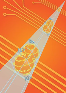
graphene polymer heterostructure

A light-sensitive graphene polymer heterostructure
Graphene is an extraordinary two-dimensional material made of a single atomic layer of carbon atoms. It is the thinnest material known to man, and yet is one of the strongest ever tested.

Graphene does not have volume, only surface – its entire structure is exposed to its environment, and responds to any molecule that touches it. This makes it in principle a very exciting material for super-sensors capable of detecting single molecules of toxic gases. Polymers can make graphene respond to specific molecules and ignore all others at the same time, which also protects it from contamination.

The research team included scientists from the National Physical Laboratory (UK), Chalmers University of Technology (Sweden), University of Copenhagen (Denmark), University of California Berkeley (USA), Linköping University (Sweden) and Lancaster University (UK). ###

The paper 'Non-volatile Photo-Chemical Gating of an Epitaxial Graphene-Polymer Heterostructure' is published in the Journal of Advanced Materials on 7th January 2011. It can be viewed here: onlinelibrary.wiley.com/doi/10.1002/

Advanced Materials. doi: 10.1002/adma.201003993

About NPL

The National Physical Laboratory (NPL) is one of the UK's leading science facilities and research centres. It is a world-leading centre of excellence in developing and applying the most accurate standards, science and technology available.

NPL occupies a unique position as the UK's National Measurement Institute and sits at the intersection between scientific discovery and real world application. Its expertise and original research have underpinned quality of life, innovation and competitiveness for UK citizens and business for more than a century. www.npl.co.uk

Contact: David Lewis david@proofcommunication.com 084-568-01865 National Physical Laboratory

Sunday, January 30, 2011

UNC researchers inch closer to unlocking potential of synthetic blood VIDEO

A team of scientists has created particles that closely mirror some of the key properties of red blood cells, potentially helping pave the way for the development of synthetic blood.

The new discovery – outlined in a study appearing in the online Early Edition of the Proceedings of the National Academy of Sciences during the week of Jan. 10, 2011 – also could lead to more effective treatments for life threatening medical conditions such as cancer.

University of North Carolina at Chapel Hill researchers used technology known as PRINT (Particle Replication in Non-wetting Templates) to produce very soft hydrogel particles that mimic the size, shape and flexibility of red blood cells, allowing the particles to circulate in the body for extended periods of time.

Tests of the particles' ability to perform functions such as transporting oxygen or carrying therapeutic drugs have not been conducted, and they do not remain in the cardiovascular system as long as real red blood cells.

However, the researchers believe the findings – especially regarding flexibility – are significant because red blood cells naturally deform in order to pass through microscopic pores in organs and narrow blood vessels. Over their 120-day lifespan, real cells gradually become stiffer and eventually are filtered out of circulation when they can no longer deform enough to pass through pores in the spleen. To date, attempts to create effective red blood cell mimics have been limited because the particles tend to be quickly filtered out of circulation due to their inflexibility.


Beyond moving closer to producing fully synthetic blood, the findings could affect approaches to treating cancer. Cancer cells are softer than healthy cells, enabling them to lodge in different places in the body, leading to the disease's spread. Particles loaded with cancer-fighting medicines that can remain in circulation longer may open the door to more aggressive treatment approaches.

synthetic blood

Extremely flexible hydrogel particles that resemble red blood cells in size and shape. To date, attempts to create effective red blood cell mimics have been limited because synthetic particles tended to be quickly filtered out of the circulatory system due to their stiffness. In testing, these flexible particles remained in circulation up to 30 times longer than stiffer ones. Image courtesy Timothy J. Merkel and Joseph M. DeSimone, University of North Carolina at Chapel Hill.
"Creating particles for extended circulation in the blood stream has been a significant challenge in the development of drug delivery systems from the beginning," said Joseph DeSimone, Ph.D., the study's co-lead investigator, Chancellor's Eminent Professor of Chemistry in UNC's College of Arts and Sciences, a member of UNC's Lineberger Comprehensive Cancer Center and William R. Kenan Jr. Distinguished Professor of Chemical Engineering at N.C. State University. "Although we will have to consider particle deformability along with other parameters when we study the behavior of particles in the human body, we believe this study represents a real game changer for the future of nanomedicine."

Chad Mirkin, Ph.D., George B. Rathmann Professor of Chemistry at Northwestern University, said the ability to mimic the natural processes of a body for medicinal purposes has been a long-standing but evasive goal for researchers. "These findings are significant since the ability to reproducibly synthesize micron-scale particles with tunable deformability that can move through the body unrestricted as do red blood cells, opens the door to a new frontier in treating disease," said Mirkin, who also is a member of President Obama's Council of Advisors on Science and Technology and director of Northwestern's International Institute for Nanotechnology.

UNC researchers designed the hydrogel material for the study to make particles of varying stiffness. Then, using PRINT technology — a technique invented in DeSimone's lab to produce nanoparticles with control over size, shape and chemistry — they created molds, which were filled with the hydrogel solution and processed to produce thousands of red blood cell-like discs, each a mere 6 micrometers in diameter.

The team then tested the particles to determine their ability to circulate in the body without being filtered out by various organs. When tested in mice, the more flexible particles lasted 30 times longer than stiffer ones: the least flexible particles disappeared from circulation with a half-life of 2.88 hours, compared to 93.29 hours for the most flexible ones. Stiffness also influenced where particles eventually ended up: more rigid particles tended to lodge in the lungs, but the more flexible particles did not; instead, they were removed by the spleen, the organ that typically removes old real red blood cells. ###

The study, "Using Mechano-biological Mimicry of Red Blood Cells to Extend Circulation Times of Hydrogel Microparticles," was led by Timothy Merkel, a graduate student in DeSimone's lab, and DeSimone. The research was made possible through a federal American Recovery and Reinvestment Act stimulus grant provided by the National Heart, Lung and Blood Institute, part of the National Institutes of Health (NIH). Support was also provided by the National Science Foundation, the Carolina Center for Cancer Nanotechnology Excellence, the NIH Pioneer Award Program and Liquidia Technologies, a privately held nanotechnology company developing vaccines and therapeutics based on the PRINT particle technology. DeSimone co-founded the company, which holds an exclusive license to the PRINT technology from UNC.

Other UNC student, faculty and staff researchers who contributed to the study are Kevin P. Herlihy and Farrell R. Kersey from the chemistry department; Mary Napier and J. Christopher Luft from the Carolina Center for Cancer Nanotechnology Excellence; Andrew Z. Wang from the Lineberger Center; Adam R. Shields from the physics department; Huali Wu and William C. Zamboni from the Institute for Pharmacogenomics and Individualized Therapy at the Eshelman School of Pharmacy; and James E. Bear and Stephen W. Jones from the cell and developmental biology department in the School of Medicine.

The study is an example of the type of research that supports the Innovate@Carolina Roadmap, UNC's plan to help Carolina become a world leader in launching university-born ideas for the good of society. To learn more about the roadmap, visit innovate.unc.edu.

Contact: Patric Lane lanep@dev.unc.edu 919-962-8596 University of North Carolina School of Medicine

Friday, January 28, 2011

Bendy tubes get around Rice-led researchers settle argument over mobility of flexible filaments

Theo Odijk, you win. The professor of biotechnology at Delft University of Technology in the Netherlands has a new best friend in Rice University's Matteo Pasquali.

Together with collaborators at the French National Center for Scientific Research (CNRS), the University of Bordeaux, France, and Vrije University, Amsterdam, the Rice professor and his team have settled a long-standing controversy in the field of polymer dynamics: The researchers proved once and for all that Odijk was correct in proclaiming that a little flexibility goes a long way for stiff filaments in a solution.

The study in the current issue of the journal Science shows that even a small ability to bend gives nanotubes and other tiny, stiff filaments the means to navigate through crowded environments, or even such fixed networks as cell matrices.

The work by Pasquali, a professor in chemical and biomolecular engineering and in chemistry, may bring about new ways to influence the motion of tiny filaments by tailoring their stiffness for a given environment.

Nanotubes are being studied for potential use in all kinds of sensing, even in the seemingly disparate fields of biological applications and oil exploration. In both, the ability of nanotubes and other fine, filamentous particles to move through their environments is critical, Pasquali said.

Matteo Pasquali

Matteo Pasquali
Understanding the motion of a single, flexible polymer chain in a network has been key to scientific advances by Odijk and others on, for example, the behavior of DNA. The Rice researchers expect their revelation to have no less impact.

Pasquali and lead author Nikta Fakhri, a former graduate student at Rice now doing postdoctoral research at the University of Gottingen, Germany, set out to break the deadlocked theories by Odijk and two other scientists who disagreed on the Brownian motion of stiff filaments in a crowded environment, and whether stiffness itself played any part.

"There's a long-standing, fundamental question: How does this threadlike object move when it gets crowded? It could be crowded because it's in a gel, or because there are a lot of threadlike objects with it -- which to that one object looks like a gel," he said.

Crowding constrains the ability of a filament to travel. Think of trying to get from the back to the front of a crowded bus; it takes a certain amount of agility to weave your way through the packed bodies. "It turns out that with a little flexibility, a filament can explore the space around it much more effectively," Pasquali said.

That becomes important when the goal is to get filaments to find and enter a cellular pore to deliver a dose of medication or to act as a fluorescent sensor.

"If you look at the human body, they say we're made of 60 percent water, but we don't slosh around," Pasquali explained. "That's because the water is trapped in pores. Almost all the water in our body is in gel-like structures: inside our cells, which are laden with filamentous networks, or in the interstitial fluid surrounding these cells. We are a big, squishy, porous medium. We need to understand how the nanoparticles move in this medium."

Pasquali and Fakhri mimicked biological networks by using varying concentrations of agarose gel, a porous material often used as a filter in biochemistry and molecular biology for DNA and proteins. The gel forms a matrix of controllable size through which molecules can move.

Nanotubes served as a stand-in for any type of filament, albeit one whose stiffness can be controlled. Like a PVC pipe in the macro world, nanotubes get stiffer as they get thicker; but even the stiffest tubes can flex a bit with length, and these tubes were thousands of times longer than they were wide.

The study started somewhat serendipitously when co-author Laurent Cognet, a researcher at CNRS and the University of Bordeaux, tried to immobilize nanotubes in agarose gels. He noticed in a failed experiment that the nanotubes moved in a "funny way" and discussed it with Pasquali.

Pasquali asked whether the nanotubes were reptating -- scientist lingo for a snakelike motion -- and Cognet said yes. Fakhri, who was studying the dynamics of nanotubes, traveled to the Bordeaux laboratory of Cognet and co-author Brahim Lounis to capture images of the nanotubes in motion.

The resulting spectroscopic and direct still and video images of 35 fluorescent single-walled nanotubes showed them snaking through the gel, probing pores and paths. The nanotubes, like all filaments, obeyed the rules of thermal-induced Brownian motion; they were pushed and pulled by the ever-changing states of the molecules around them.

The research established that flexibility significantly enhances the nanotubes' ability to navigate around obstacles and speeds up their exploration.

Pasquali said Fakhri doggedly pursued her analysis of the nanotubes' motion through computerized image recognition and motion tracking, as well as old-fashioned pencil-and-paper dynamical analysis. He said his longtime collaborator, co-author Frederick MacKintosh, a theoretical physicist at Vrije University, was a tremendous help. MacKintosh has been studying the dynamics of biological networks for nearly two decades.

Pasquali intends to replace the gel with real rocks to see how nanotubes, which can be used as oil-detecting sensors, move in a more structured environment. "Rocks can be a little more complicated," he said. "The question here is, what can nanotubes do better than nanoparticles? The answer may be that slender nanotubes may interact with electromagnetic fields more strongly than other nanoparticles of the same volume."

The National Science Foundation Center for Biological and Environmental Nanotechnology, the Welch Foundation, the Advanced Energy Consortium, the Région Aquitaine, the Agence National pour la Recherche, the European Research Council and the Dutch Foundation for Fundamental Research on Matter supported the work.

Contact: David Ruth druth@rice.edu 713-348-6327 Rice University

Graphene grains make atom-thick patchwork quilts as Cornell scientists find their electrical and mechanical properties

ITHACA - Artistry from science: Cornell University researchers have unveiled striking, atomic-resolution details of what graphene “quilts” look like at the boundaries between patches, and have uncovered key insights into graphene’s electrical and mechanical properties.

Researchers focused on graphene – a one atom-thick sheet of carbon atoms bonded in a crystal lattice like a honeycomb or chicken wire – because of its electrical properties and potential to improve everything from solar cells to cell phone screens.

But graphene doesn’t grow in perfect sheets. Rather, it develops in pieces that resemble patchwork quilts, where the honeycomb lattice meets up imperfectly. These “patches” meet at grain boundaries, and scientists had wondered whether these boundaries would allow the special properties of a perfect graphene crystal to transfer to the much larger quilt-like structures.

To study the material, the researchers grew graphene membranes on a copper substrate (a method devised by another group) but then conceived a novel way to peel them off as free-standing, atom-thick films.

several grains in graphene

A false-color microscopy image overlay depicting the shapes and lattice orientations of several grains in graphene. IMAGE: The Energy Materials Center at Cornell
Then with diffraction imaging electron microscopy, they imaged the graphene by seeing how electrons bounced off at certain angles, and using a color to represent that angle. By overlaying different colors according to how the electrons bounced, they created an easy, efficient method of imaging the graphene grain boundaries according to their orientation. And as a bonus, their pictures took an artistic turn, reminding the scientists of patchwork quilts.

“You don’t want to look at the whole quilt by counting each thread. You want to stand back and see what it looks like on the bed. And so we developed a method that filters out the crystal information in a way that you don’t have to count every atom,” said David Muller, professor of applied and engineering physics and co-director of the Kavli Institute at Cornell for Nanoscale Science.

Muller conducted the work with Paul McEuen, professor of physics and director of the Kavli Institute, and Kavli member Jiwoong Park, assistant professor of chemistry and chemical biology.

Further analysis revealed that growing larger grains (bigger patches) didn’t improve the electrical conductivity of the graphene, as was previously thought by materials scientists. Rather, it is impurities that sneak into the sheets that make the electrical properties fluctuate. This insight will lead scientists closer to the best ways to grow and use graphene.

The work was supported by the National Science Foundation through the Cornell Center for Materials Research and the Nanoscale Science and Engineering Initiative. The paper’s other contributors were: Pinshane Huang, Carlos Ruiz-Vargas, Arend van der Zande, William Whitney, Mark Levendorf, Shivank Garg, JonathanAlden and Ye Zhu, all from Cornell; Joshua Kevek, Oregon State University and Caleb Hustedt, Brigham Young University.
Contact: Blaine Friedlander bpf2@cornell.edu 607-254-8093 Cornell University
Thursday, January 27, 2011

New solar cell self-repairs like natural plant systems

WEST LAFAYETTE, Ind. - Researchers are creating a new type of solar cell designed to self-repair like natural photosynthetic systems in plants by using carbon nanotubes and DNA, an approach aimed at increasing service life and reducing cost.

"We've created artificial photosystems using optical nanomaterials to harvest solar energy that is converted to electrical power," said Jong Hyun Choi, an assistant professor of mechanical engineering at Purdue University.

The design exploits the unusual electrical properties of structures called single-wall carbon nanotubes, using them as "molecular wires in light harvesting cells," said Choi, whose research group is based at the Birck Nanotechnology and Bindley Bioscience centers at Purdue's Discovery Park.

"I think our approach offers promise for industrialization, but we're still in the basic research stage," he said.

Photoelectrochemical cells convert sunlight into electricity and use an electrolyte - a liquid that conducts electricity - to transport electrons and create the current. The cells contain light-absorbing dyes called chromophores, chlorophyll-like molecules that degrade due to exposure to sunlight.

Jong Hyun Choi and Benjamin Baker

Caption: Jong Hyun Choi, an assistant professor of mechanical engineering at Purdue, and doctoral student Benjamin Baker use fluorescent imaging to view a carbon nanotube. Their research is aimed at creating a new type of solar cell designed to self-repair like natural photosynthetic systems. The approach might enable researchers to increase the service life and reduce costs for photoelectrochemical cells, which convert sunlight into electricity.

Credit: Purdue University photo/Mark Simons. Usage Restrictions: None.
"The critical disadvantage of conventional photoelectrochemical cells is this degradation," Choi said.

The new technology overcomes this problem just as nature does: by continuously replacing the photo-damaged dyes with new ones.

"This sort of self-regeneration is done in plants every hour," Choi said.

The new concept could make possible an innovative type of photoelectrochemical cell that continues operating at full capacity indefinitely, as long as new chromophores are added.

Findings were detailed in a November presentation during the International Mechanical Engineering Congress and Exhibition in Vancouver. The concept also was unveiled in an online article (spie.org/x41475) featured on the Web site for SPIE, an international society for optics and photonics.

The talk and article were written by Choi, doctoral students Benjamin A. Baker and Tae-Gon Cha, and undergraduate students M. Dane Sauffer and Yujun Wu.

The carbon nanotubes work as a platform to anchor strands of DNA. The DNA is engineered to have specific sequences of building blocks called nucleotides, enabling them to recognize and attach to the chromophores.

"The DNA recognizes the dye molecules, and then the system spontaneously self-assembles," Choi said

When the chromophores are ready to be replaced, they might be removed by using chemical processes or by adding new DNA strands with different nucleotide sequences, kicking off the damaged dye molecules. New chromophores would then be added.

Two elements are critical for the technology to mimic nature's self-repair mechanism: molecular recognition and thermodynamic metastability, or the ability of the system to continuously be dissolved and reassembled.

The research is an extension of work that Choi collaborated on with researchers at the Massachusetts Institute of Technology and the University of Illinois. The earlier work used biological chromophores taken from bacteria, and findings were detailed in a research paper published in November in the journal Nature Chemistry (www.nature.com/nchem/journal/v2/).

However, using natural chromophores is difficult, and they must be harvested and isolated from bacteria, a process that would be expensive to reproduce on an industrial scale, Choi said.

"So instead of using biological chromophores, we want to use synthetic ones made of dyes called porphyrins," he said. ###

Writer: Emil Venere, 765-494-4709, venere@purdue.edu Source: Jong Hyun Choi, 765-496-3562, jchoi@purdue.edu Related website: Jong Hyun Choi: engineering.purdue.edu/~jchoi/

Abstract on the research in this release is available at: www.purdue.edu/newsroom/research/2011/

Contact: Emil Venere venere@purdue.edu 765-494-4709 Purdue University

New glaucoma test allows earlier, more accurate detection

TUCSON, Ariz. -- Cumbersome glaucoma tests requiring a visit to the ophthalmologist could soon be history thanks to a home test developed by an engineer at the University of Arizona.

A new hand-held instrument involving a system of micro-force sensors, specially designed microchips, and math-based programmed procedures has been designed by researchers at the UA College of Engineering. The easy-to-use probe gently rubs the eyelid and can be used at home, threatening to replace painful eye drops and the need for a sterilized sensor.

"You simply close your eye and rub the eyelid like you might casually rub your eye," said Eniko Enikov, professor of aerospace and mechanical engineering and head of the Advanced Micro and Nanosystems Laboratory at the University of Arizona's College of Engineering. "The instrument detects the stiffness and, therefore, infers the intraocular pressure," Enikov said.

Work on the probe began four years ago in collaboration with Dr. Gholan Peyman, a Phoenix ophthalmologist. The instrument went through several years of refinement and modifications to arrive at the current design, a prototype instrument that's noninvasive and simpler than current procedures.

Dr. Gholan Peyman

Phoenix ophthalmologist Dr. Gholan Peyman demonstrates a prototype glaucoma test instrument that's noninvasive and simpler to use than current procedures. It can also be used in situations that are difficult or impossible with current tests.
It can also be used in situations that are difficult or impossible with current tests.

In addition to screening for glaucoma -- an eye disease that can lead to blindness if left untreated -- the device can be used to measure drainage of intraocular fluid. Patients could use the probe at home to trace how much the pressure decreases after using eye drop medications.

According to the Glaucoma Research Foundation, glaucoma is a leading cause of blindness. There is no cure, everyone is at risk, and there may be no symptoms to warn you. More than 4 million Americans have glaucoma but only half know they have it.

The development work was funded through the National Science Foundation, and Enikov and Peyman now are seeking investors to help fund final development and commercialization of the product.

"The innovation with our device is that it's noninvasive, simpler to use and applies to a variety of situations that are either difficult to address or impossible to test using the current procedures," Enikov said. "That's why we're so excited about this probe. It has great potential to improve medical care, and significant commercial possibilities, as well." ###

More information about the new glaucoma test instrument can be found at the University of Arizona College of Engineering website here www.engr.arizona.edu/news/story.php?id=225

More on the Advanced Micro and Nanosystems Laboratory can be found here nano.arizona.edu/ and more information on glaucoma, current research and treatments can be found here www.glaucoma.org/

Contact: Steve Delgado sdelgado@engr.arizona.edu 520-621-2815
University of Arizona College of Engineering

Wednesday, January 26, 2011

'Nanoscoops' could spark new generation of electric automobile batteries

New nanoengineered batteries developed at Rensselaer exhibit remarkable power density, charging more than 40 times faster than today's lithium-ion batteries.

Troy, N.Y. – An entirely new type of nanomaterial developed at Rensselaer Polytechnic Institute could enable the next generation of high-power rechargeable lithium (Li)-ion batteries for electric automobiles, as well as batteries for laptop computers, mobile phones, and other portable devices.

The new material, dubbed a "nanoscoop" because its shape resembles a cone with a scoop of ice cream on top, can withstand extremely high rates of charge and discharge that would cause conventional electrodes used in today's Li-ion batteries to rapidly deteriorate and fail. The nanoscoop's success lies in its unique material composition, structure, and size.

The Rensselaer research team, led by Professor Nikhil Koratkar, demonstrated how a nanoscoop electrode could be charged and discharged at a rate 40 to 60 times faster than conventional battery anodes, while maintaining a comparable energy density. This stellar performance, which was achieved over 100 continuous charge/discharge cycles, has the team confident that their new technology holds significant potential for the design and realization of high-power, high-capacity Li-ion rechargeable batteries.

Nanoscoops

Nanoscoops

Nanoscoops

Caption: Researchers at Rensselaer Polytechnic Institute developed an entirely new type of nanomaterial that could enable the next generation of high-power rechargeable lithium (Li)-ion batteries for electric automobiles, laptop computers, mobile phones and other devices. The material, called a "nanoscoop" because it resembles a cone with a scoop of ice cream on top, is shown in the above scanning electron microscope image. Nanoscoops can withstand extremely high rates of charge and discharge that would cause today's Li-ion batteries to rapidly deteriorate and fail.

Credit: Rensselaer/Koratkar. Usage Restrictions: Please include image credit.
"Charging my laptop or cell phone in a few minutes, rather than an hour, sounds pretty good to me," said Koratkar, a professor in the Department of Mechanical, Aerospace, and Nuclear Engineering at Rensselaer. "By using our nanoscoops as the anode architecture for Li-ion rechargeable batteries, this is a very real prospect. Moreover, this technology could potentially be ramped up to suit the demanding needs of batteries for electric automobiles."

Batteries for all-electric vehicles must deliver high power densities in addition to high energy densities, Koatkar said. These vehicles today use supercapacitors to perform power-intensive functions, such as starting the vehicle and rapid acceleration, in conjunction with conventional batteries that deliver high energy density for normal cruise driving and other operations. Koratkar said the invention of nanoscoops may enable these two separate systems to be combined into a single, more efficient battery unit.

Results of the study were detailed in the paper "Functionally Strain-Graded Nanoscoops for High Power Li-Ion Battery Anodes," published Thursday by the journal Nano Letters. See the full paper at: pubs.acs.org/doi/abs/10.1021/

The anode structure of a Li-ion battery physically grows and shrinks as the battery charges or discharges. When charging, the addition of Li ions increases the volume of the anode, while discharging has the opposite effect. These volume changes result in a buildup of stress in the anode. Too great a stress that builds up too quickly, as in the case of a battery charging or discharging at high speeds, can cause the battery to fail prematurely. This is why most batteries in today's portable electronic devices like cell phones and laptops charge very slowly – the slow charge rate is intentional and designed to protect the battery from stress-induced damage.

The Rensselaer team's nanoscoop, however, was engineered to withstand this buildup of stress. Made from a carbon (C) nanorod base topped with a thin layer of nanoscale aluminum (Al) and a "scoop" of nanoscale silicon (Si), the structures are flexible and able to quickly accept and discharge Li ions at extremely fast rates without sustaining significant damage. The segmented structure of the nanoscoop allows the strain to be gradually transferred from the C base to the Al layer, and finally to the Si scoop. This natural strain gradation provides for a less abrupt transition in stress across the material interfaces, leading to improved structural integrity of the electrode.

The nanoscale size of the scoop is also vital since nanostructures are less prone to cracking than bulk materials, according to Koratkar.

"Due to their nanoscale size, our nanoscoops can soak and release Li at high rates far more effectively than the macroscale anodes used in today's Li-ion batteries," he said. "This means our nanoscoop may be the solution to a critical problem facing auto companies and other battery manufacturers – how can you increase the power density of a battery while still keeping the energy density high?"

A limitation of the nanoscoop architecture is the relatively low total mass of the electrode, Koratkar said. To solve this, the team's next steps are to try growing longer scoops with greater mass, or develop a method for stacking layers of nanoscoops on top of each other. Another possibility the team is exploring includes growing the nanoscoops on large flexible substrates that can be rolled or shaped to fit along the contours or chassis of the automobile. ###

Along with Koratkar, authors on the paper are Toh-Ming Lu, the R.P. Baker Distinguished Professor of Physics and associate director of the Center for Integrated Electronics at Rensselaer; and Rahul Krishnan, a graduate student in the Department of Materials Science and Engineering at Rensselaer.

This study was supported by the National Science Foundation (NSF) and the New York State Energy Research and Development Authority (NYSERDA).

For more information on Koratkar's research at Rensselaer, visit:

For more information on Lu's research at Rensselaer, visit:

Contact: Michael Mullaney. Rensselaer Polytechnic Institute. Troy, NY 518-276-6161 mullam@rpi.edu, www.rpi.edu/news

Visit the Rensselaer research and discovery blog: approach.rpi.edu

Follow us on Twitter: www.twitter.com/RPInews

Monday, January 24, 2011

Einstein-Montefiore researcher will test nanoparticles against pancreatic cancer

(BRONX, NY) ─ A five-year, $16-million grant from the National Cancer Institute will take advantage of specialized expertise developed by scientists at Albert Einstein College of Medicine of Yeshiva University and Montefiore, the University Hospital and Academic Medical Center for Einstein. The research – carried out by a group of five institutions, including Einstein, that comprise the Texas Center for Cancer Nanomedicine – could lead to novel ways to diagnose and treat pancreatic and ovarian cancer using nanoparticles.

Nanoparticles are engineered materials that are 100 nanometers or less in size. (A nanometer is one billionth of a meter.) Nanoparticles impregnated with drugs are called nanomedicines.

"We will be investigating nanomedicines for both imaging and treating pancreatic tumors," said Einstein-Montefiore principal investigator Steven Libutti, M.D., professor and vice chair of surgery at Einstein and Montefiore, director of the Montefiore-Einstein Center for Cancer Care, and associate director for clinical services of the Albert Einstein Cancer Center. "Our part of the consortium is developing nanoparticles that will specifically target unique aspects of the blood vessels found in pancreatic adenocarcinomas and pancreatic neuroendocrine tumors."

Steven Libutti, M.D

Steven Libutti, M.D
Pancreatic cancer is the fourth-leading cause of all cancer deaths. Currently, there is no test for early detection of the disease, which killed nearly 37,000 people in 2010. Only 5.6 percent of people diagnosed with pancreatic cancer live for five years or longer, according to the National Cancer Institute.

Dr. Libutti has developed mice that are genetically programmed to form pancreatic tumors that mimic those seen in people. These mice will be used for testing a variety of nanoparticle-based drugs produced by other collaborators.
Such studies will reveal whether the particles can home in on disease locations and deliver therapeutic benefits. Dr. Libutti's clinical practice involves the surgical management of patients with cancer, including those with pancreatic cancer. A main focus of his research is the formation of new blood vessels that nourish tumors.

Identifying the most promising nanoparticle-based drugs for pancreatic as well as ovarian cancer will take several years. Clinical trials are not likely to begin until the end of the five-year project.

###

In addition to Einstein the other institutions that are members of the Texas Center for Cancer Nanomedicine involved in the nanotech consortium are the University of Texas MD Anderson Cancer Center, the University of Texas Health Science Center at Houston, the Methodist Hospital Research Institute, and Rice University.

About Albert Einstein College of Medicine of Yeshiva University

Albert Einstein College of Medicine of Yeshiva University is one of the nation's premier centers for research, medical education and clinical investigation. During the 2009-2010 academic year, Einstein is home to 722 M.D. students, 243 Ph.D. students, 128 students in the combined M.D./Ph.D. program, and approximately 350 postdoctoral research fellows. The College of Medicine has 2,775 fulltime faculty members located on the main campus and at its clinical affiliates. In 2009, Einstein received more than $155 million in support from the NIH.

This includes the funding of major research centers at Einstein in diabetes, cancer, liver disease, and AIDS. Other areas where the College of Medicine is concentrating its efforts include developmental brain research, neuroscience, cardiac disease, and initiatives to reduce and eliminate ethnic and racial health disparities. Through its extensive affiliation network involving five medical centers in the Bronx, Manhattan and Long Island - which includes Montefiore Medical Center, The University Hospital and Academic Medical Center for Einstein - the College of Medicine runs one of the largest post-graduate medical training programs in the United States, offering approximately 150 residency programs to more than 2,500 physicians in training. For more information, please visit www.einstein.yu.edu

Contact: Kim Newman sciencenews@einstein.yu.edu 718-430-3101 Albert Einstein College of Medicine

Sunday, January 23, 2011

Purdue, NIST working on breathalyzers for medical diagnostics

WEST LAFAYETTE, Ind. — Researchers have overcome a fundamental obstacle in developing breath-analysis technology to rapidly diagnose patients by detecting chemical compounds called "biomarkers" in a person's respiration in real time.

The researchers demonstrated their approach is capable of rapidly detecting biomarkers in the parts per billion to parts per million range, at least 100 times better than previous breath-analysis technologies, said Carlos Martinez, an assistant professor of materials engineering at Purdue who is working with researchers at the National Institute of Standards and Technology.

"People have been working in this area for about 30 years but have not been able to detect low enough concentrations in real time," he said. "We solved that problem with the materials we developed, and we are now focusing on how to be very specific, how to distinguish particular biomarkers."

The technology works by detecting changes in electrical resistance or conductance as gases pass over sensors built on top of "microhotplates," tiny heating devices on electronic chips. Detecting biomarkers provides a record of a patient's health profile, indicating the possible presence of cancer and other diseases.

Sensor for Advanced Breath-analysis Technology

Caption: This image shows a new type of sensor for an advanced breath-analysis technology that rapidly diagnoses patients by detecting "biomarkers" in a person's respiration in real time. Researchers used a template made of micron-size polymer particles and coated them with much smaller metal oxide nanoparticles. Using nanoparticle-coated microparticles instead of a flat surface allows researchers to increase the porosity of the sensor films, increasing the "active sensing surface area" to improve sensitivity.

Credit: Purdue University and NIST. Usage Restrictions: None.
"We are talking about creating an inexpensive, rapid way of collecting diagnostic information about a patient," Martinez said. "It might say, 'there is a certain percentage that you are metabolizing a specific compound indicative of this type of cancer,' and then additional, more complex tests could be conducted to confirm the diagnosis."

The researchers used the technology to detect acetone, a biomarker for diabetes, with a sensitivity in the parts per billion range in a gas mimicking a person's breath.

Findings were detailed in a research paper that appeared earlier this year in the IEEE Sensors Journal, published by the Institute of Electrical and Electronics Engineers' IEEE Sensors Council. The paper was co-authored by Martinez and NIST researchers Steve Semancik, lead author Kurt D. Benkstein, Baranidharan Raman and Christopher B. Montgomery.

The researchers used a template made of micron-size polymer particles and coated them with far smaller metal oxide nanoparticles.
Using nanoparticle-coated microparticles instead of a flat surface allows researchers to increase the porosity of the sensor films, increasing the "active sensing surface area" to improve sensitivity.

A droplet of the nanoparticle-coated polymer microparticles was deposited on each microhotplate, which are about 100 microns square and contain electrodes shaped like meshing fingers. The droplet dries and then the electrodes are heated up, burning off the polymer and leaving a porous metal-oxide film, creating a sensor.

"It's very porous and very sensitive," Martinez said. "We showed that this can work in real time, using a simulated breath into the device."

Gases passing over the device permeate the film and change its electrical properties depending on the particular biomarkers contained in the gas.

Such breathalyzers are likely a decade or longer away from being realized, in part because precise standards have not yet been developed to manufacture devices based on the approach, Martinez said.

"However, the fact that we were able to do this in real time is a big step in the right direction," he said. ###

Writer: Emil Venere, 765-494-4709, venere@purdue.edu Source: Carlos Martinez, 765-494-3271, cjmartinez@purdue.edu Related website: Carlos Martinez: engineering.purdue.edu/MSE/

Abstract on the research in this release is available at: www.purdue.edu/newsroom/research/2010/

Contact: Emil Venere venere@purdue.edu 765-494-4709 Purdue University

Saturday, January 22, 2011

Texas A&M professor helps develop first high-temp spin-field-effect transistor

COLLEGE STATION, — An international team of researchers featuring Texas A&M University physicist Jairo Sinova has announced a breakthrough that gives a new spin to semiconductor nanoelectronics and the world of information technology.

The team has developed an electrically controllable device whose functionality is based on an electron's spin. Their results, the culmination of a 20-year scientific quest involving many international researchers and groups, are published in the current issue of Science.

The team, which also includes researchers from the Hitachi Cambridge Laboratory and the Universities of Cambridge and Nottingham in the United Kingdom as well as the Academy of Sciences and Charles University in the Czech Republic, is the first to combine the spin-helix state and anomalous Hall effect to create a realistic spin-field-effect transistor (FET) operable at high temperatures, complete with an AND-gate logic device — the first such realization in the type of transistors originally proposed by Purdue University's Supriyo Datta and Biswajit Das in 1989.

"One of the major stumbling blocks was that to manipulate spin, one may also destroy it," Sinova explains. "It has only recently been realized that one could manipulate it without destroying it by choosing a particular set-up for the device and manipulating the material. One also has to detect it without destroying it, which we were able to do by exploiting our findings from our study of the spin Hall effect six years ago. It is the combination of these basic physics research projects that has given rise to the first spin-FET."

spin-Hall injection device

spin-Hall injection device used as a base for the spin-field-effect transistor
Sixty years after the transistor's discovery, its operation is still based on the same physical principles of electrical manipulation and detection of electronic charges in a semiconductor, says Hitachi's Dr. Jorg Wunderlich, senior researcher in the team. He says subsequent technology has focused on down-scaling the device size, succeeding to the point where we are approaching the ultimate limit, shifting the focus to establishing new physical principles of operation to overcome these limits — specifically, using its elementary magnetic movement, or so-called "spin," as the logic variable instead of the charge.
This new approach constitutes the field of "spintronics," which promises potential advances in low-power electronics, hybrid electronic-magnetic systems and completely new functionalities.

Wunderlich says the 20-year-old theory of electrical manipulation and detection of electron's spin in semiconductors — the cornerstone of which is the "holy grail" known as the spin transistor — has proven to be unexpectedly difficult to experimentally realize.

"We used recently discovered quantum-relativistic phenomena for both spin manipulation and detection to realize and confirm all the principal phenomena of the spin transistor concept," Wunderlich explains.

To observe the electrical manipulation and detection of spins, the team made a specially designed planar photo-diode (as opposed to the typically used circularly polarized light source) placed next to the transistor channel. By shining light on the diode, they injected photo-excited electrons, rather than the customary spin-polarized electrons, into the transistor channel. Voltages were applied to input-gate electrodes to control the procession of spins via quantum-relativistic effects. These effects — attributable to quantum relativity — are also responsible for the onset of transverse electrical voltages in the device, which represent the output signal, dependent on the local orientation of processing electron spins in the transistor channel.

The new device can have a broad range of applications in spintronics research as an efficient tool for manipulating and detecting spins in semiconductors without disturbing the spin-polarized current or using magnetic elements.

Wunderlich notes the observed output electrical signals remain large at high temperatures and are linearly dependent on the degree of circular polarization of the incident light. The device therefore represents a realization of an electrically controllable solid-state polarimeter which directly converts polarization of light into electric voltage signals. He says future applications may exploit the device to detect the content of chiral molecules in solutions, for example, to measure the blood-sugar levels of patients or the sugar content of wine.

This work forms part of wider spintronics activity within Hitachi worldwide, which expects to develop new functionalities for use in fields as diverse as energy transfer, high-speed secure communications and various forms of sensor.

While Wunderlich acknowledges it is yet to be determined whether or not spin-based devices will become a viable alternative to or complement of their standard electron-charge-based counterparts in current information-processing devices, he says his team's discovery has shifted the focus from the theoretical academic speculation to prototype microelectronic device development.

"For spintronics to revolutionize information technology, one needs a further step of creating a spin amplifier," Sinova says. "For now, the device aspect — the ability to inject, manipulate and create a logic step with spin alone — has been achieved, and I am happy that Texas A&M University is a part of that accomplishment." ###

To learn more about the team's research, go to faculty.physics.tamu.edu/sinova/.

Sinova, (979) 845-4179 or sinova@physics.tamu.edu

About research at Texas A&M University: As one of the world's leading research institutions, Texas A&M is in the vanguard in making significant contributions to the storehouse of knowledge, including that of science and technology. Research conducted at Texas A&M represents an annual investment of more than $630 million, which ranks third nationally for universities without a medical school, and underwrites approximately 3,500 sponsored projects. That research creates new knowledge that provides basic, fundamental and applied contributions resulting in many cases in economic benefits to the state, nation and world.

Contact: Shana K. Hutchins, (979) 862-1237 or shutchins@science.tamu.edu or Dr. Jairo

Contact: Jairo Sinova sinova@physics.tamu.edu 979-845-4179 Texas A&M University

Friday, January 21, 2011

TU scientists in Nature: Better control of building blocks for quantum computer

Scientists from the Kavli Institute of Nanoscience at Delft University of Technology and Eindhoven University of Technology in The Netherlands have succeeded in controlling the building blocks of a future super-fast quantum computer. They are now able to manipulate these building blocks (qubits) with electrical rather than magnetic fields, as has been the common practice up till now. They have also been able to embed these qubits into semiconductor nanowires. The scientists' findings have been published in the current issue of the science journal Nature (23 December).

Spin

A qubit is the building block of a possible, future quantum computer, which would far outstrip current computers in terms of speed. One way to make a qubit is to trap a single electron in semiconductor material. A qubit can, just like a normal computer bit, adopt the states '0' and '1'. This is achieved by using the spin of an electron, which is generated by spinning the electron on its axis. The electron can spin in two directions (representing the '0' state and the '1' state).

Electrical instead of magnetic

Until now, the spin of an electron has been controlled by magnetic fields. However, these field are extremely difficult to generate on a chip.

nanowire qubits

Caption: This is an artist's impression of nanowire qubits.

Credit: Gemma Plum. Usage Restrictions: None.
The electron spin in the qubits that are currently being generated by the Dutch scientists can be controlled by a charge or an electric field, rather than by magnetic fields. This form of control has major advantages, as Leo Kouwenhoven, scientist at the Kavli Institute of Nanoscience at TU Delft, points out: 'These spin-orbit qubits combine the best of both worlds. They employ the advantages of both electronic control and information storage in the electron spin.'

Nanowires

There is another important new development in the Dutch research: the scientists have been able to embed the qubits (two) into nanowires made of a semiconductor material (indium arsenide). These wires are of the order of nanometres in diameter and micrometres in length. Kouwenhoven: 'These nanowires are being increasingly used as convenient building blocks in nanoelectronics.
Nanowires are an excellent platform for quantum information processing, among other applications.' ###

Contact: Leo Kouwenhoven l.p.kouwenhoven@tudelft.nl 31-152-786-064 Delft University of Technology

Wednesday, January 19, 2011

Ever-sharp urchin teeth may yield tools that never need honing

MADISON – To survive in a tumultuous environment, sea urchins literally eat through stone, using their teeth to carve out nooks where the spiny creatures hide from predators and protect themselves from the crashing surf on the rocky shores and tide pools where they live.

The rock-boring behavior is astonishing, scientists agree, but what is truly remarkable is that, despite constant grinding and scraping on stone, urchin teeth never, ever get dull. The secret of their ever-sharp qualities has puzzled scientists for decades, but now a new report by scientists from the University of Wisconsin-Madison and their colleagues has peeled back the toothy mystery.

Writing today (Dec. 22, 2010) in the journal Advanced Functional Materials, a team led by UW-Madison professor of physics Pupa Gilbert describes the self-sharpening mechanism used by the California purple sea urchin to keep a razor-sharp edge on its choppers.

The urchin's self-sharpening trick, notes Gilbert, is something that could be mimicked by humans to make tools that never need honing.

California purple sea urchins

New research by Pupa Gilbert, a physics professor at UW-Madison, and her colleagues reveals how the sea urchin’s teeth are always sharp, despite constant grinding and scraping to create the nooks that protect the marine animal from predators and crashing waves. Top: California purple sea urchins are pictured in the rocky tide-pool hideaways that they carve with their teeth.

Photo: Jeff Miller.
"The sea urchin tooth is complicated in its design. It is one of the very few structures in nature that self-sharpen," says Gilbert, explaining that the sea urchin tooth, which is always growing, is a biomineral mosaic composed of calcite crystals with two forms – plates and fibers – arranged crosswise and cemented together with super-hard calcite nanocement. Between the crystals are layers of organic materials that are not as sturdy as the calcite crystals.

"The organic layers are the weak links in the chain," Gilbert explains. "There are breaking points at predetermined locations built into the teeth. It is a concept similar to perforated paper in the sense that the material breaks at these predetermined weak spots."

The crystalline nature of sea urchin dentition is, on the surface, different from other crystals found in nature.
It lacks the obvious facets characteristic of familiar crystals, but at the very deepest levels the properties of crystals are evident in the orderly arrangement of the atoms that make up the biomineral mosaic teeth of the sea urchin.

To delve into the fundamental nature of the crystals that form sea urchin teeth, Gilbert and her colleagues used a variety of techniques from the materials scientist's toolbox. These include microscopy methods that depend on X-rays to illuminate how nanocrystals are arranged in teeth to make the sea urchins capable of grinding rock. Gilbert and her colleagues used these techniques to deduce how the crystals are organized and melded into a tough and durable biomineral.

Knowing the secret of the ever-sharp sea urchin tooth, says Gilbert, could one day have practical applications for human toolmakers. "Now that we know how it works, the knowledge could be used to develop methods to fabricate tools that could actually sharpen themselves with use," notes Gilbert. "The mechanism used by the urchin is the key. By shaping the object appropriately and using the same strategy the urchin employs, a tool with a self-sharpening edge could, in theory, be created." ###

The new research was supported by grants from the U.S. Department of Energy and the National Science Foundation. In addition to Gilbert, researchers from the University of California, Berkeley; Argonne National Laboratory; the Weizmann Institute of Science; and the Lawrence Berkeley National Laboratory contributed to the report.

Contact: Pupa Gilbert pupa@physics.wisc.edu 608-358-0164 University of Wisconsin-Madison

Eindhoven University builds affordable alternative to mega-laser X-FEL

Stanford University in the USA has an X-FEL (X-ray Free Electron Laser) with a pricetag of hundreds of millions. It provides images of 'molecules in action', using a kilometer-long electron accelerator. Researchers at Eindhoven University of Technology (TU/e) have developed an alternative that can do many of the same things. However this alternative fits on a tabletop, and costs around half a million euro. That's why the researchers have jokingly called it 'the poor man's X-FEL'.

It's one of the few remaining 'holy grails' of science: a system that allows you to observe the extremely high-speed molecular processes at an atomic scale. You could call it an ultra-fast video microscope. Instead of visible light this kind of system uses X-rays or electrons, because it requires radiation with a wavelength of less than a nanometer. The X-rays or electrons have to be emitted in ultra short pulses, so that the exposure time is extremely short. However these pulses are not easy to generate. An X FEL uses X-ray pulses for this purpose, generated by accelerating electrons in an accelerator of a kilometer, or longer. These electrons are then converted into X-rays. An installation of this kind is very costly, uses large amounts of energy and needs a whole team to operate it. A European X-FEL, which will cost a billion euro, is currently under construction in Hamburg (Germany).

One centimeter

Thijs van Oudheusden, Eindhoven University of Technology

Caption: Thijs van Oudheusden stands with his "poor man's X-FEL."

Credit: Photo: Bart van Overbeeke. Usage Restrictions: None.
TU/e doctoral candidate ir. Thijs van Oudheusden (Department of Applied Physics) has developed a machine that in many respects can compete with this billion-euro facility, based on ideas from his co supervisor dr.ir. Jom Luiten. The essence of their 'poor man's X-FEL' is that it uses electrons instead of X-rays. "Why convert electrons into X-rays if you can use the electrons themselves?", asks Van Oudheusden. "As well as that you only need to give the electrons a low energy, so you can accelerate them in just a centimeter. That's why the whole system fits on a tabletop."

Just one shot

The physical barrier that Van Oudheusden had to overcome is that the electrons in electron bunches repel each other. This causes the electron bunches to expand, making them longer than the desired 100 femtoseconds (1 femtosecond is 10-15 second), which in turn would make the 'video microscope' too slow. Jom Luiten thought of a solution to prevent the undesired expansion. The key was to create bunches of exactly the right shape, so they can be controlled and focused by means of electrical fields into bunches of the desired type and length. All with a number of electrons (1 million) that is sufficient to create a diffraction pattern in just a single shot.

In users' own labs

Supervisor prof.dr. Marnix van der Wiel believes that half to three-quarters of the kind of research that can be done on an X-FEL can also be done with the 'poor man's X_FEL'. But this doesn't immediately mean that the latter is automatically a lot cheaper in relation to the scientific output that can be generated with it. "The X-FEL at Stanford works non-stop, all year round, and is used by thousands of research groups over several decades. So if you're allocated time on the system you have to take all your equipment to the USA, where you have to stick to a very strict schedule. Our finding is a good alternative for people who want to have the freedom to do research in their own labs. As far as the costs are concerned, it depends on the user if our system will turn out to be cheaper on a per publication basis."

Half a million

TU/e spin-off AccTec BV intends to build the machine developed by Van Oudheusden and Luiten and to sell it to scientific users. AccTec expects the total price to be below half a million euro.

Thijs van Oudheusden gained his PhD on 13 December with his doctoral thesis entitled 'Electron source for sub-relativistic single-shot femtosecond diffraction'. His research received financial support from the Stichting voor Fundamenteel Onderzoek der Materie (Foundation for Fundamental Research on Matter – FOM). ###

Contact: Ivo Jongsma i.l.a.jongsma@tue.nl 31-402-472-110 Eindhoven University of Technology

Tuesday, January 18, 2011

Strange new twist: Berkeley researchers discover Möbius symmetry in metamaterials

Möbius symmetry, the topological phenomenon that yields a half-twisted strip with two surfaces but only one side, has been a source of fascination since its discovery in 1858 by German mathematician August Möbius. As artist M.C. Escher so vividly demonstrated in his "parade of ants," it is possible to traverse the "inside" and "outside" surfaces of a Möbius strip without crossing over an edge. For years, scientists have been searching for an example of Möbius symmetry in natural materials without any success. Now a team of scientists has discovered Möbius symmetry in metamaterials – materials engineered from artificial "atoms" and "molecules" with electromagnetic properties that arise from their structure rather than their chemical composition.

Xiang Zhang, a scientist with the U.S. Department of Energy's Lawrence Berkeley National Laboratory (Berkeley Lab) and a professor at the University of California (UC) Berkeley, led a study in which electromagnetic Möbius symmetry was successfully introduced into composite metamolecular systems made from metals and dielectrics. This discovery opens the door to finding and exploiting novel phenomena in metamaterials.

"We have experimentally observed a new topological symmetry in electromagnetic metamaterial systems that is equivalent to the structural symmetry of a Möbius strip, with the number of twists controlled by sign changes in the electromagnetic coupling between the meta-atoms," Zhang says.

Mobius symmetry in Metamaterials

Caption: Berkeley Lab researcher have discovered Möbius symmetry in metamolecular trimers made from metals and dielectrics.

Credit: Image by Chih-Wei Chang. Usage Restrictions: None.

Xiang Zhang, DOE/Lawrence Berkeley National Laboratory

Caption: Xiang Zhang is a faculty scientist with Berkeley Lab and UC Berkeley.

Credit: Photo by Roy Kaltschmidt, Berkeley Lab Public Affairs. Usage Restrictions: None.
"We have further demonstrated that metamaterials with different coupling signs exhibit resonance frequencies that depend on the number but not the locations of the twists. This confirms the topological nature of the symmetry."

Working with metallic resonant meta-atoms configured as coupled split-ring resonators, Zhang and members of his research group assembled three of these meta-atoms into trimers. Through careful design of the electromagnetic couplings between the constituent meta-atoms, these trimers displayed Möbius C3 symmetry – meaning Möbius cyclic symmetry through three rotations of 120 degrees. The Möbius twists result from a change in the signs of the electromagnetic coupling constants between the constituent meta-atoms.

"The topological Möbius symmetry we found in our meta-molecule trimers is a new symmetry not found in naturally occurring materials or molecules." Zhang says. "Since the coupling constants of metamolecules can be arbitrarily varied from positive to negative without any constraints, the number of Möbius twists we can introduce are unlimited. This means that topological structures that have thus far been limited to mathematical imagination can now be realized using metamolecules of different designs."

Details on this discovery have been published in the journal Physical Review Letters, in a paper titled "Optical Möbius Symmetry in Metamaterials." Co-authoring the paper with Zhang were Chih-Wei Chang, Ming Liu, Sunghyun Nam, Shuang Zhang, Yongmin Liu and Guy Bartal.

Xiang Zhang is a principal investigator with Berkeley Lab's Materials Sciences Division and the Ernest S. Kuh Endowed Chaired Professor at UC Berkeley, where he directs the Center for Scalable and Integrated NanoManufacturing (SINAM), a National Science Foundation Nano-scale Science and Engineering Center.

In science, symmetry is defined as a system feature or property that is preserved when the system undergoes a change.
This is one of the most fundamental and crucial concepts in science, underpinning such physical phenomena as the conservation laws and selection rules that govern the transition of a system from one state to another. Symmetry also dictates chemical reactions and drives a number of important scientific tools, including crystallography and spectroscopy.

While some symmetries, such as spatial geometries, are easily observed, others, such as optical symmetries, may be hidden. A powerful investigative tool for uncovering hidden symmetries is a general phenomenon known as "degeneracy." For example, the energy level degeneracy of an atom in a crystal is correlated with the crystal symmetry. A three-body system, like a trimer, can be especially effective for studying the correlation between degeneracy and symmetry because, although it is a relatively simple system, it reveals a rich spectrum of phenomena.

"The unique properties of a three-body system make experimental investigations of hidden symmetries possible," says Chih-Wei Chang, a former post-doc in Zhang's group and the lead author of the paper in Physical Review Letters, says. "Intrigued by the extraordinary engineering flexibilities of metamaterials, we decided to investigate some non-trivial symmetries hidden beneath these metamolecules by studying their degeneracy properties"

The authors tested their metamaterials for hidden symmetry by shining a light and monitoring the optical resonances. The resulting resonant frequencies revealed that degeneracy is kept even when the coupling constants between meta-atoms flip signs.

"Because degeneracy and symmetry are always correlated, there must be some symmetry hidden beneath the observed degeneracy" says Chang.

The researchers showed that whereas trimer systems with uniform negative (or positive) coupling signs could be symbolized as an equilateral triangle, trimer systems with mixed signs of couplings could only be symbolized as a Möbius strip with topological C3 symmetry. Furthermore, in other metamolecular systems made of six meta-atoms, the authors demonstrated up to three Möbius twists.

Says Chang, now a faculty member at National Taiwan University in Taipei, "When going from natural systems to artificial meta-atoms and metamolecules, we can expect to encounter phenomena far beyond our conventional conceptions. The new symmetries we find in metamaterials could be extended to other kinds of artificial systems, such as Josephson junctions, that will open new avenues for novel phenomena in quantum electronics and quantum optics." ###

This research was supported by the DOE Office of Science and by the NSF's Nano-scale Science and Engineering Center.

Lawrence Berkeley National Laboratory is a U.S. Department of Energy (DOE) national laboratory managed by the University of California for the DOE Office of Science. Berkeley Lab provides solutions to the world's most urgent scientific challenges including sustainable energy, climate change, human health, and a better understanding of matter and force in the universe. It is a world leader in improving our lives through team science, advanced computing, and innovative technology. Visit our at www.lbl.gov

Contact: Lynn Yarris lcyarris@lbl.gov 510-486-5375 DOE/Lawrence Berkeley National Laboratory

UCSB scientists demonstrate biomagnification of nanomaterials in simple food chain

(Santa Barbara, Calif.) –– An interdisciplinary team of researchers at UC Santa Barbara has produced a groundbreaking study of how nanoparticles are able to biomagnify in a simple microbial food chain.

"This was a simple scientific curiosity," said Patricia Holden, professor in UCSB's Bren School of Environmental Science & Management and the corresponding author of the study, published in an early online edition of the journal Nature Nanotechnology. "But it is also of great importance to this new field of looking at the interface of nanotechnology and the environment."

Holden's co-authors from UCSB include Eduardo Orias, research professor of genomics with the Department of Molecular, Cellular and Developmental Biology; Galen Stucky, professor of chemistry and biochemistry, and materials; and graduate students, postdoctoral scholars, and staff researchers Rebecca Werlin, Randy Mielke, John Priester, and Peter Stoimenov. Other co-authors are Stephan Krämer, from the California Nanosystems Institute, and Gary Cherr and Susan Jackson, from the UC Davis Bodega Marine Laboratory.

Quantum Dot-Tainted Bacteria Stop Digestion in the Protozoan

Caption: The quantum dot-tainted bacteria stop digestion in the protozoan, and food vacuoles with undigested material accumulate, seen in the right image. This is in contrast to the normal condition of protozoa eating untreated bacteria, seen in the left image.

Credit: UCSB. Usage Restrictions: None.
The research was partially funded by the U.S. Environmental Protection Agency (EPA) STAR Program, and by the UC Center for the Environmental Implications of Nanotechnology (UC CEIN), a $24 million collaboration based at UCLA, with researchers from UCSB, UC Davis, UC Riverside, Columbia University, and other national and international partners. UC CEIN is funded by the National Science Foundation and the EPA.

According to Holden, a prior collaboration with Stucky, Stoimenov, Priester, and Mielke provided the foundation for this research. In that earlier study, the researchers observed that nanoparticles formed from cadmium selenide were entering certain bacteria (called Pseudomonas) and accumulating in them.
"We already knew that the bacteria were internalizing these nanoparticles from our previous study," Holden said. "And we also knew that Ed (Orias) and Rebecca (Werlin) were working with a protozoan called Tetrahymena and nanoparticles. So we approached them and asked if they would be interested in a collaboration to evaluate how the protozoan predator is affected by the accumulated nanoparticles inside a bacterial prey." Orias and Werlin credit their interest in nanoparticle toxicity to earlier funding from and participation in the University of California Toxic Substance Research & Training Program.

The scientists repeated the growth of the bacteria with quantum dots in the new study and and coupled it to a trophic transfer study –– the study of the transfer of a compound from a lower to a higher level in a food chain by predation. "We looked at the difference to the predator as it was growing at the expense of different prey types –– 'control' prey without any metals, prey that had been grown with a dissolved cadmium salt, and prey that had been grown with cadmium selenide quantum dots," Holden said.

What they found was that the concentration of cadmium increased in the transfer from bacteria to protozoa and, in the process of increasing concentration, the nanoparticles were substantially intact, with very little degradation. "We were able to measure the ratio of the cadmium to the selenium in particles that were inside the protozoa and see that it was substantially the same as in the original nanoparticles that had been used to feed the bacteria," Orias said.

The fact that the ratio of cadmium and selenide was preserved throughout the course of the study indicates that the nanoparticles were themselves biomagnified. "Biomagnification –– the increase in concentration of cadmium as the tracer for nanoparticles from prey into predator –– this is the first time this has been reported for nanomaterials in an aquatic environment, and furthermore involving microscopic life forms, which comprise the base of all food webs," Holden said.

An implication is that nanoparticles inside the protozoa could then be available to the next level of predators in the food chain, which could lead to broader ecological effects. "These protozoa are greatly enriched in nanoparticles because of feeding on quantum dot-laced bacteria," Hold said. "Because there were toxic effects on the protozoa in this study, there is a concern that there could also be toxic effects higher in the food chain, especially in aquatic environments."

One of the missions of UC CEIN is to try to understand the effects of nanomaterials in the environment, and how scientists can prevent any possible negative effects that might pose a threat to any form of life. "In this context, one might argue that if you could 'design out' whatever property of the quantum dots causes them to enter bacteria, then we could avoid this potential consequence," Holden said. "That would be a positive way of viewing a study like this. Now scientists can look back and say, 'How do we prevent this from happening?' " ###

Contact: George Foulsham 805-893-3071 University of California - Santa Barbara

Monday, January 17, 2011

Your genome in minutes: New technology could slash sequencing time

Imperial scientists are developing technology that could lead to ultrafast DNA sequencing tool within ten years

Scientists from Imperial College London are developing technology that could ultimately sequence a person's genome in mere minutes, at a fraction of the cost of current commercial techniques.

The researchers have patented an early prototype technology that they believe could lead to an ultrafast commercial DNA sequencing tool within ten years. Their work is described in a study published this month in the journal 'Nano Letters' and it is supported by the Wellcome Trust Translational Award and the Corrigan Foundation.

The research suggests that scientists could eventually sequence an entire genome in a single lab procedure, whereas at present it can only be sequenced after being broken into pieces in a highly complex and time-consuming process. Fast and inexpensive genome sequencing could allow ordinary people to unlock the secrets of their own DNA, revealing their personal susceptibility to diseases such as Alzheimer's, diabetes and cancer. Medical professionals are already using genome sequencing to understand population-wide health issues and research ways to tailor individualised treatments or preventions.

genome-sequencing chip

Close-up image of prototype genome-sequencing chip.
Dr Joshua Edel, one of the authors on the study from the Department of Chemistry at Imperial College London, said: "Compared with current technology, this device could lead to much cheaper sequencing: just a few dollars, compared with $1m to sequence an entire genome in 2007. We haven't tried it on a whole genome yet but our initial experiments suggest that you could theoretically do a complete scan of the 3,165 million bases in the human genome within minutes, providing huge benefits for medical tests, or DNA profiles for police and security work. It should be significantly faster and more reliable, and would be easy to scale up to create a device with the capacity to read up to 10 million bases per second, versus the typical 10 bases per second you get with the present day single molecule real-time techniques."

In the new study, the researchers demonstrated that it is possible to propel a DNA strand at high speed through a tiny 50 nanometre (nm) hole - or nanopore - cut in a silicon chip, using an electrical charge. As the strand emerges from the back of the chip, its coding sequence (bases A, C, T or G) is read by a 'tunnelling electrode junction'. This 2 nm gap between two wires supports an electrical current that interacts with the distinct electrical signal from each base code. A powerful computer can then interpret the base code's signal to construct the genome sequence, making it possible to combine all these well-documented techniques for the first time.

Sequencing using nanopores has long been considered the next big development for DNA technology, thanks to its potential for high speed and high-capacity sequencing. However, designs for an accurate and fast reader have not been demonstrated until now.

Co-author Dr Emanuele Instuli, from the Department of Chemistry at Imperial College London, explained the challenges they faced in this research: "Getting the DNA strand through the nanopore is a bit like sucking up spaghetti. Until now it has been difficult to precisely align the junction and the nanopore. Furthermore, engineering the electrode wires with such dimensions approaches the atomic scale and is effectively at the limit of existing instrumentation. However in this experiment we were able to make two tiny platinum wires into an electrode junction with a gap sufficiently small to allow the electron current to flow between them."

This technology would have several distinct advantages over current techniques, according to co-author, Aleksandar Ivanov from the Department of Chemistry at Imperial College London: "Nanopore sequencing would be a fast, simple procedure, unlike available commercial methods, which require time-consuming and destructive chemical processes to break down and replicate small sections of the DNA molecules to determine their sequence. Additionally, these silicon chips are incredibly durable compared with some of the more delicate materials currently used. They can be handled, washed and reused many times over without degrading their performance."

Dr Tim Albrecht, another author on the study, from the Department of Chemistry at Imperial College London, says: "The next step will be to differentiate between different DNA samples and, ultimately, between individual bases within the DNA strand (ie true sequencing). I think we know the way forward, but it is a challenging project and we have to make many more incremental steps before our vision can be realised." ###

Contact: Simon Levey s.levey@imperial.ac.uk 44-020-759-46702 Imperial College London

Sunday, January 16, 2011

German federal government bolsters neutron research in Garching

300 million euros for the Garching research neutron source.

The German Federal Ministry of Education and Research (BMBF) will fund the scientific use of the neutron source Heinz Maier-Leibnitz (FRM II) by German and international researchers to the tune of 198 million euros over the next ten years. The Helmholtz Research Centers Juelich, Berlin, and Geesthacht are contributing a further 105.2 million euros from their budgets. The basis for these grants is the cooperation between the Technische Universitaet Muenchen (TUM) as operator of the FRM II and the Helmholtz Centers leading to joint scientific use of the neutron source.

The framework for this cooperation is set out in an administrative agreement between the German Federal Government and the State of Bavaria. The head of the Bavarian State Ministry of Science, Research and the Arts, Dr. Friedrich Wilhelm Rothenpieler, and the head of the Department for Basic Research at the BMBF, Dr. Karl Eugen Huthmacher, signed the agreement today in Garching. The cooperation contract itself was also signed today by TUM President Professor Wolfgang A. Herrmann, Member of the Board of the Forschungszentrum Juelich Professor Ulrich Krafft, Scientific Director of the Helmholtz Center Geesthacht Professor Wolfgang Kaysser, and Scientific Director of the Helmholtz Center Berlin Professor Anke Pyzalla-Kaysser.

Signing of TUM-Helmholtz Cooperation Contract

Caption: The official signing of the contract for cooperation between the research neutron source FRM II and the Helmholtz research centers Juelich, Geeshacht, and Berlin took place on Dec. 17, 2010, in the Institute for Advanced Study of the Technische Universitaet Muenchen (TUM). Front row, left to right: Thomas Frederking (authorized officer, Helmholtz Center Berlin), Dr. Ulrich Krafft (Acting Chairman, Forschungszentrum Juelich), Prof. Dr. Dr. h.c. mult. Wolfgang A. Herrmann (TU Muenchen President), Prof. Dr.-Ing. Anke Pyzalla-Kaysser (Scientific Executive Director, Helmholtz Center Berlin), Prof. Dr. Wolfgang Kaysser (Scientific Technical Director, Helmholtz Center Geesthacht), Prof. Dr. Andreas Schreyer (Material Physics Director, Helmholtz Center Geesthacht). Standing, left to right: Prof. Dr. Dieter Richter (Director of the Institute for Solid-State Research, Forschungszentrum Juelich), Ministerial Director Dr. Karl Eugen Huthmacher (German Federal Ministry of Education and Research), Ministerial Director Dr. Wilhelm Friedrich Rothenpieler (Bavarian State Ministry of Sciences, Research, and the Arts), Prof. Dr. Winfried Petry (Scientific Director of FRM II, TU Muenchen), Albert Berger (Chancellor, TU Muenchen)..

Credit: Copyright TU Muenchen. Usage Restrictions: This photo may be freely used, with copyright noted, in news coverage of TU Muenchen.

Research Neutron Source FRM II

Caption: The research neutron source Heinz Maier-Leibnitz (FRM II), operated by the Technische Universitaet Muenchen in Garching, Germany.

Credit: TU Muenchen. Usage Restrictions: This photo may be freely used, with copyright noted, in news coverage of TU Muenchen.
The contract stipulates that the German Federal Government will finance the scientific use of the FRM II via the Helmholtz Centers with 19.8 million euros per year. In addition, the three Helmholtz Centers under the auspices of the Forschungszentrum Juelich (FZ Juelich) will invest 10.52 million euros annually for neutron research. The contract will run over a period of ten years.

Neutrons are used to conduct research on the functions of complex materials such as proteins, superconductors, and materials for energy storage. "The multifaceted capabilities of the Garching neutron source will attain a new quality through the cooperation between the TUM, as the responsible operator, and the three Helmholz Centers," says TUM President Professor Wolfgang A. Hermann. "The foundation for this cooperation is the unrivaled performance spectrum of our neutron source, which attracts researchers from across the globe. A joint chair with the Forschungszentrum Juelich in the field of neutron research would round things off perfectly."

Pursuant to this agreement, the TU Muenchen and the three Helmholtz Centers will operate the FRM II jointly for scientific uses in the future. The Technische Universitaet Muenchen remains the sole operator of the neutron source itself. That is why the State of Bavaria will continue to fund reactor operation and research with 25 million euros annually.

FRM II Scientific Director Professor Winfried Petry is proud of the awarded grant: "The involvement of the Helmholtz Centers and the BMBF is the best evidence that we are already performing exceptionally well. The FRM II provides researchers with neutron beams of the utmost brilliance and its instruments lead the pack. This grant will provide us with the opportunity to exploit the potential of the neutron source even better in supporting top level German and international research."

Concretely, the grant will be used to build new instruments, to upgrade existing instruments, and to increase technical and scientific staff. New office and laboratory space will also need to be created for the additional personnel. Currently, 24 instruments at the FRM II are already at the disposal of guest scientists from around the world. The number of large-scale instruments will rise to over 30 in the near future. Measurement slots at the FRM II are in high demand. They are overbooked at more than twice the available capacity and are awarded via an application system based on scientific excellence and run by independent experts.

The cooperation contract is an extension to a cooperation agreement from 2004 with the FZ Juelich, which has set up its own branch at the FRM II.
The Helmholtz Centers Juelich, Geesthacht and Berlin have been involved in the development and operation of large-scale scientific instruments at the neutron source in Garching. Juelich is leading the way with five instruments in operation at the FRM II, and five more to follow. The Centers Geestacht and Berlin have two instruments and one instrument respectively. The Max Planck Society also has two instruments. The TUM will operate 14 instruments, with a further instrument run jointly with the FZ Juelich. Furthermore, groups from seven other German universities are participating in the instrumentation. Their commitment will also be funded by the BMBF in the context of collective research. ###

Contact: Professor Winfried Petry Technische Universitaet Muenchen Neutron Source Heinz Maier-Leibnitz 85748 Garching, Germany Tel.: +49 89 289 14704 Fax: +49 89 289 14995 E-mail: winfried.petry@frm2.tum.de Internet: www.frm2.tum.de

Technische Universitaet Muenchen (TUM) is one of Europe's leading universities. It has roughly 460 professors, 7,500 academic and non-academic staff (including those at the university hospital "Rechts der Isar"), and 26,000 students. It focuses on the engineering sciences, natural sciences, life sciences, medicine, and economic sciences. After winning numerous awards, it was selected as an "Elite University" in 2006 by the Science Council (Wissenschaftsrat) and the German Research Foundation (DFG). The university's global network includes an outpost in Singapore. TUM is dedicated to the ideal of a top-level research based entrepreneurial university. www.tum.de