Sunday, October 31, 2010

Turn common acrylic paint into insulation with nanotechnology VIDEO


Turn common acrylic paint into insulation with nanotechnology.

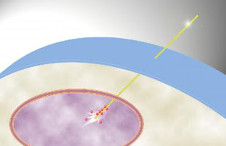
Exciting technology by NanoPhos ThermoDry turn normal paint into an insulating barrier by reflecting the infra-red spectrum and reducing conduction by 4 times.

Category: Science & Technology
Tags: insulation nanotechnology paint conductivity reflection thermodry nanophos

VIDEO and TEXT CREDIT: knewbill

New graphene fabrication method uses silicon carbide templates to create desired growth

Smoothing the edges

Researchers at the Georgia Institute of Technology have developed a new "templated growth" technique for fabricating nanometer-scale graphene devices. The method addresses what had been a significant obstacle to the use of this promising material in future generations of high-performance electronic devices.

The technique involves etching patterns into the silicon carbide surfaces on which epitaxial graphene is grown. The patterns serve as templates directing the growth of graphene structures, allowing the formation of nanoribbons of specific widths without the use of e-beams or other destructive cutting techniques. Graphene nanoribbons produced with these templates have smooth edges that avoid electron-scattering problems.

"Using this approach, we can make very narrow ribbons of interconnected graphene without the rough edges," said Walt de Heer, a professor in the Georgia Tech School of Physics.

graphene transistors

Using a new "templated growth" technique, researchers have fabricated an array of 10,000 graphene transistors.
"Anything that can be done to make small structures without having to cut them is going to be useful to the development of graphene electronics because if the edges are too rough, electrons passing through the ribbons scatter against the edges and reduce the desirable properties of graphene."
The new technique has been used to fabricate an array of 10,000 top-gated graphene transistors on a 0.24 square centimeter chip – believed to be the largest density of graphene devices reported so far.

The research was reported Oct. 3 in the advance online edition of the journal Nature Nanotechnology. The work was supported by the National Science Foundation, the W.M. Keck Foundation and the Nanoelectronics Research Initiative Institute for Nanoelectronics Discovery and Exploration (INDEX).

In creating their graphene nanostructures, De Heer and his research team first use conventional microelectronics techniques to etch tiny "steps" – or contours – into a silicon carbide wafer. They then heat the contoured wafer to approximately 1,500 degrees Celsius, which initiates melting that polishes any rough edges left by the etching process.

They then use established techniques for growing graphene from silicon carbide by driving off the silicon atoms from the surface. Instead of producing a consistent layer of graphene one atom thick across the surface of the wafer, however, the researchers limit the heating time so that graphene grows only on the edges of the contours.

To do this, they take advantage of the fact that graphene grows more rapidly on certain facets of the silicon carbide crystal than on others. The width of the resulting nanoribbons is proportional to the depth of the contour, providing a mechanism for precisely controlling the nanoribbons. To form complex graphene structures, multiple etching steps can be carried out to create a complex template, de Heer explained.

"By using the silicon carbide to provide the template, we can grow graphene in exactly the sizes and shapes that we want," he said. "Cutting steps of various depths allows us to create graphene structures that are interconnected in the way we want them to be.

In nanometer-scale graphene ribbons, quantum confinement makes the material behave as a semiconductor suitable for creation of electronic devices. But in ribbons a micron or more wide, the material acts as a conductor. Controlling the depth of the silicon carbide template allows the researchers to create these different structures simultaneously, using the same growth process.

"The same material can be either a conductor or a semiconductor depending on its shape," noted de Heer, who is also a faculty member in Georgia Tech's National Science Foundation-supported Materials Research Science and Engineering Center (MRSEC). "One of the major advantages of graphene electronics is to make the device leads and the semiconducting ribbons from the same material. That's important to avoid electrical resistance that builds up at junctions between different materials."

After formation of the nanoribbons – which can be as narrow as 40 nanometers – the researchers apply a dielectric material and metal gate to construct field-effect transistors. While successful fabrication of high-quality transistors demonstrates graphene's viability as an electronic material, de Heer sees them as only the first step in what could be done with the material.

"When we manage to make devices well on the nanoscale, we can then move on to make much smaller and finer structures that will go beyond conventional transistors to open up the possibility for more sophisticated devices that use electrons more like light than particles," he said. "If we can factor quantum mechanical features into electronics, that is going to open up a lot of new possibilities."

De Heer and his research team are now working to create smaller structures, and to integrate the graphene devices with silicon. The researchers are also working to improve the field-effect transistors with thinner dielectric materials.

Ultimately, graphene may be the basis for a generation of high-performance devices that will take advantage of the material's unique properties in applications where the higher cost can be justified. Silicon will continue to be used in applications that don't require such high performance, de Heer said.

"This is another step showing that our method of working with epitaxial graphene on silicon carbide is the right approach and the one that will probably be used for making graphene electronics," he added. "This is a significant new step toward electronics manufacturing with graphene." ###

In addition to those already mentioned, the research has involved M. Sprinkle, M. Ruan, Y Hu, J. Hankinson, M. Rubio-Roy, B. Zhang, X. Wu and C. Berger.

Research News & Publications Office Georgia Institute of Technology 75 Fifth Street, N.W., Suite 314 Atlanta, Georgia 30308 USA

Contact: John Toon jtoon@gatech.edu 404-894-6986 Georgia Institute of Technology Research News

Thursday, October 28, 2010

Breakthrough e-Display means electronics with high speed, high readability and low power usage

Oct. 4 issue of the high-impact journal, Applied Physics Letters, contains a new electrofluidics design from the University of Cincinnati and start-up company Gamma Dynamics that promises to dramatically reshape the image capabilities of electronic devices.

This patent-pending electrofluidics breakthrough by the Novel Devices Laboratory at the University of Cincinnati and partner companies Gamma Dynamics, Dupont and Sun Chemical follows about seven years of work. According to lead researcher Jason Heikenfeld, UC associate professor of electrical and computer engineering in the College of Engineering & Applied Science, and John Rudolph, president of Gamma Dynamics, the breakthrough is even more impressive when you realize that similar research efforts elsewhere have lasted a decade without achieving similar results.

Importantly, this new "zero power" e-Design from UC can be manufactured with existing equipment and technology.

How New e-Display Technology Works

Caption: The two horizontal "boxes" above represent views of the new technology design -- with the pigment dispersion fluid represented as "in motion." Ambient light enters via the device screen. When that light hits the layer of reflective electrodes, it is amplified.

Credit: Jason Heikenfeld and Angela Klocke, U. of Cincinnati. Usage Restrictions: None.
Said Heikenfeld, "What we've developed breaks down a significant barrier to bright electronic displays that don't require a heavy battery to power them."

He explained that, currently, electronic devices fall into two basic camps. The first includes those devices that offer limited function and slow speed but require little power to operate. These would include e-readers like the Kindle.

In the second camp, devices like cell phones, laptops and the iPad provide high color saturation and high-speed capability for video and other functions but at a cost of high power usage.

Heikenfeld stated, "Conventional wisdom says you can't have it all with electronic devices: speed, brightness and low-cost manufacturing. That's going to change with the introduction of this new discovery into the market. This idea has been in the works for a while, but we did not start really pushing the project until we thought we could make it manufacturable."
A NEW DESIGN THAT MAKES USE OF REFLECTION

Before describing UC's new "zero-power" design, it's helpful to understand the basic design of existing electronic devices.

Think of an e-reader as a bunch of micro-sized buckets (or pixels) of mixed black and white paint, where you can move the black and white pigments to the top or the bottom of the bucket. Just like mixing paint, the process is not fast. That's somewhat close to how today's e-readers work. The slow movement of these particles forms the text and grayscale images you see on an e-reader. These devices use practically no power unless you are switching the screen. It's actually making use of ambient light to make the particles visible. When the user turns the device on or off or switches a page, he's electronically "mixing the paint" (or pixels) to create the overall image or text page.

Faster, color-saturated, high-power devices like a computer's liquid-crystal display screen, an iPad or a cell phone require high power, in part, because they need a strong internal light source within the device (that "backlights" the screen) as well as color filters in order to display the particles as color/moving images. The need for an internal light source within the device also means visibility is poor in bright, natural light.

The new "zero-power" design combines the best features of both these kinds of devices. It requires low-power because it makes use of ambient light vs. a strong, internal light source within the device. As such and because of its low-power requirements, this new technology will make for more environmentally friendly electronic devices, stated Heikenfeld.

Yet, even though an electronic device with this eletrofluidic technology would lack a strong, internal light source, it would still display bright images at high speed. How?

Behind the display screen are two layers of liquid (oil and a pigment dispersion fluid like an inkjet fluid). Between the two layers are reflective electrodes. Think of these electrodes as a highly reflective mirror.

Ambient light enters through the display screen and through the first layer of liquid and hits the reflective electrodes. When the light hits that reflective electrode, it bounces back out to the viewer's eye, creating the perception of a bright, color-saturated image…or text or video… .

A small electric charge powers the movement of these oil and pigment-dispersion liquids. The movement occurs between a bottom layer behind the reflective electrodes and a top layer in front of the reflective electrodes. When the pigmented substance is positioned in the "top" layer (sandwiched between the ambient light and reflective electrodes), it creates a reflected ray of colored light which combines with literally millions of ambient light rays to produce a full-color display.

(The closest competition with similar brightness is electrochromic technology, which does not switch quickly enough to create video images. And the closest competition that is really low power but can still "do" video is called "Mirasol" technology developed by Quallcomm. However, when trying to display a color like white, the "Mirasol" technology has about one-third the brightness level of the UC technology being announced today. "Mirasol," in fact, resembles greyed newsprint.)

THIS NEW TECHNOLOGY IS MANUFACTURABLE WITH CURRENT FACILITIES AND EQUIPMENT

Importantly, the new e-Display design published today is manufacturable with current facilities and technology.

Manufacturability using the same equipment as that used for current LCDs was essential since a new LCD plant costs around $2 billion.

WHEN WILL THIS TECHNOLOGY BE AVAILABLE TO CONSUMERS

According to Gamma Dynamics' Rudolph, this electrofluidics breakthrough will change the display technology used in a myriad of electronic devices. e-Readers like the Amazon Kindle will be able to display color and video. Devices like cell phones and iPads will require much less power and will be readable even in bright sunlight.

He estimated consumers will likely first see it in action as grocery-store shelf labels and advertising displays in about three years' time.

Currently, liquid-crystal displays are attached to some grocery-store shelves, providing product and price information. These run on battery power; however, the batteries are insufficient to meet the LCDs' high power requirements. So, their brightness levels are insufficient to attract shoppers' attention. Stores still attach paper labels to them in order to indicate sale items or barcodes with eye-catching brightness.

Rudolph said that by substituting the UC-developed electrofluidic e-Display technology, these shelf-label devices would become bright and eye-catching. Given the frequency with which shelf labels are updated, the store labels should then operate for at least five years without the need for battery replacement. ###

RESEARCH SUPPORT

As mentioned, Gamma Dynamics, Dupont and Sun Chemical partnered with UC in this research. Partial support was also provided by grants from the National Science Foundation, the Army Research Laboratory and the Air Force Research Laboratory.

Contact: M.B. Reilly reillymb@ucmail.uc.edu 513-556-1824 University of Cincinnati

Wednesday, October 27, 2010

NIH awards $14.6M nanomedicine center created to detect and treat atherosclerosis

Georgia Tech and Emory University have received a five-year $14.6 million contract from the National Institutes of Health (NIH) to continue the development of nanotechnology and biomolecular engineering tools and methodologies for detecting and treating atherosclerosis.

Atherosclerosis typically occurs in branched or curved regions of arteries where plaques form because of cholesterol build-up. Inflammation can alter the structure of plaques so they become more likely to rupture, potentially causing a blood vessel blockage and leading to heart attack or stroke.

The award will support the interdisciplinary Center for Translational Cardiovascular Nanomedicine as the second phase of the Program of Excellence in Nanotechnology (PEN), originally established in 2005 with funding from the National Heart, Lung, and Blood Institute of the NIH. This Center integrates the biomedical engineering expertise of Georgia Tech and the cardiology strengths of Emory University's School of Medicine. The broad and long-term goal of the PEN is to improve the diagnosis and treatment of cardiovascular disease, which is the leading cause of death for men and women in the United States.

Gang Bao, Georgia Tech

Caption: Gang Bao, director of the Center for Translational Cardiovascular Nanomedicine, received $14.6 million from the National Institutes of Health to lead a research team in developing nanotechnology and biomolecular engineering tools and methodologies for detecting and treating atherosclerosis.

Credit: Georgia Tech Photo: Gary Meek. Usage Restrictions: None.
"In the last five years, we developed a suite of nanotechnology approaches for diagnosing and treating cardiovascular disease and we have demonstrated their efficacy in terms of potential clinical application," said Gang Bao, the program's director and the Robert A. Milton Chair in Biomedical Engineering in the Wallace H. Coulter Department of Biomedical Engineering at Georgia Tech and Emory University. "For the next five years, we will focus on translating these technologies into clinical utility and we would like to have some of these nanotechnologies ready for human clinical trials by the end of this five-year period."

During the first five years of the PEN, the Georgia Tech and Emory University researchers have made contributions in nanotechnology development, basic cardiology research and inflammatory biomarker detection.
The research team has published or submitted more than 80 peer-reviewed papers, filed nine patents and established three startup companies to commercialize the nanotechnologies.

"There is a great unmet need to develop innovative diagnostic modalities that inform the activity of the inflammatory disease and to guide evaluation of therapy," explained Bao, who is also a Georgia Tech College of Engineering Distinguished Professor. "Our nanotechnology toolbox will allow us to translate more mature nanotechnologies to clinical utility and evaluate new nanotechnologies that will provide unique functionalities and novel applications."

The second phase of the PEN will build on the foundation developed and progress made during the last five years to accomplish four goals:

* Using nanoparticle probes to image and characterize atherosclerotic plaques
* Diagnosing cardiovascular disease from a blood sample
* Designing new methods for delivering anti-atherosclerosis drugs and genes into the body
* Developing stem cell based therapies to repair damaged heart tissue

The researchers will use the suite of nanotechnologies they developed in the last five years -- including molecular beacons, magnetic nanoparticles, gold nanoparticles, quantum dots, polyketals and hydrocyanine dyes -- to accomplish these goals.

The first goal focuses on determining if an individual's atherosclerotic plaque will grow and rupture. Having this information would allow physicians to treat atherosclerosis more effectively.

"By using nanoparticle probes in vitro and in vivo, we hope to be able to detect early-stage cardiovascular disease," noted Bao, "but many important issues such as detection specificity, toxicity and safety still need to be addressed."

In addition to in vivo imaging of plaques using magnetic resonance imaging (MRI) and positron emission tomography (PET), the research team is developing a laboratory diagnostic test for detecting cardiovascular disease from a blood sample. The presence or levels of specific micro-RNAs, reactive oxygen species or protein markers in the blood will be tested as an indication of the presence and stage of atherosclerosis. This diagnostic approach has the advantages of being fast, inexpensive and nontoxic.

Once atherosclerosis is detected in an individual, it needs to be treated. Several small molecule drugs have been identified as potent therapeutic agents for cardiovascular diseases, but their clinical utility is limited due to their water-repellant nature and short circulation half-life. A novel approach for targeted drug or gene delivery is to use nanoparticles to carry the small molecules into the body. This type of delivery system has the advantage of combining targeting, imaging and controlled release, and can be tailored to optimize circulation time and reduce toxicity.

"Delivering these small molecules in a specific, sufficient and sustained manner to localized vascular lesions may significantly improve the clinical outcomes of cardiovascular diseases," said Bao.

For the final goal, the research team will use stem cells to create a personalized treatment strategy for repairing damage caused by atherosclerosis. The researchers plan to use nanotechnologies to generate and deliver patient-specific induced pluripotent stem cells to the injured vasculature and heart to repair the damage.

"Our goals are ambitious as we plan to further develop our nanoscale tools and nanocardiology knowledge base, to translate the new tools and nanotechnologies to clinical applications in diagnosing and treating cardiovascular disease, and to train the next generation of leaders in cardiovascular nanomedicine," added Bao. ###

Also contributing from the Coulter Department are professors Don Giddens, Xiaoping Hu, Hanjoong Jo, Shuming Nie, and W. Robert Taylor; associate professors Niren Murthy and May Dongmei Wang; and assistant professor Michael Davis. Giddens is also dean of Georgia Tech's College of Engineering. Taylor is also the director of Emory's Division of Cardiology and a member of the Atlanta VA Medical Center's Division of Cardiology.

Contributors from Emory University include Department of Medicine chair Wayne Alexander; Division of Cardiology professors David Harrison and Kathy Griendling, associate professor Young-sup Yoon and assistant professor Charles Searles Jr.; and Department of Radiology professor Mark Goodman. Katherine Ferrara, a biomedical engineering professor at the University of California, Davis, is also collaborating on the project.

Contact: Abby Vogel Robinson abby@innovate.gatech.edu 404-385-3364 Georgia Institute of Technology Research News

Tuesday, October 26, 2010

DNA art imitates life: Construction of a nanoscale Mobius strip

The enigmatic Möbius strip has long been an object of fascination, appearing in numerous works of art, most famously a woodcut by the Dutchman M.C. Escher, in which a tribe of ants traverses the form's single, never-ending surface.

Scientists at the Biodesign Institute at Arizona State University's and Department of Chemistry and Biochemistry, led by Hao Yan and Yan Liu, have now reproduced the shape on a remarkably tiny scale, joining up braid-like segments of DNA to create Möbius structures measuring just 50 nanometers across—roughly the width of a virus particle.

Eventually, researchers hope to capitalize on the unique material properties of such nano-architectures, applying them to the development of biological and chemical sensing devices, nanolithography, drug delivery mechanisms pared down to the molecular scale and a new breed of nanoelectronics.

DNA Kirigami

Caption: A Möbius strip cut along its centerline, yields a Kirigami-Ring.

Credit: Nature Nanotechnology. Usage Restrictions: None.
The team used a versatile construction method known as DNA origami and in a dramatic extension of the technique, (which they refer to as DNA Kirigami), they cut the resulting Möbius shapes along their length to produce twisted ring structures and interlocking loops known as catenanes.

Their work appears in today's advanced online issue of the journal Nature Nanotechnology. Graduate students involved in this work include Dongran Han and Suchetan Pal in the Yan group

Making a Möbius strip in the everyday world is easy. Cut a narrow strip of paper, bring the two ends of the strip close to each other so that they match, but give them a half-twist before fastening the ends together with a piece of scotch tape. The resulting Möbius strip, which has only one surface and one boundary edge, is an example of a topological form.

"As nanoarchitects," Yan says, "we strive to create two classes of structure—geometric and topological." Geometric structures in two and three dimensions abound in the natural world, from complex crystal shapes to starfish, and unicellular organisms like diatoms.
Yan cites such natural forms as a boundless source of inspiration for human-designed nanostructures.

Topology, a branch of mathematics, describes the spatial properties of shapes that may be twisted, stretched or otherwise deformed to yield new shapes. Such shape deformations may profoundly alter the geometry of an object, as when a donut shape is pinched and stretched into a figure eight, but the surface topology of such forms is unaffected.

Nature is also rich in topological structures, Yan notes, including the elegant Möbius. The circulations of earth's warmer and cooler ocean currents for example, describe a Möbius shape. Other topological structures are common to biological systems, particularly in the case of DNA, the 3 billion chemical bases of which are packed by the chromosome inside the cell, using topological structures. "In bacteria, plasmid DNA is wound into a supercoil," Yan explains. "Then the enzymes can come in and cut and reconfigure the topology to relieve the torsion in the supercoil so that all the other cellular machinery can have access to the gene for replication, transcription and so forth."

To form the Möbius strip in the current study, the group relied on properties of self-assembly inherent in DNA. A strand of DNA is formed from combinations of 4 nucleotide bases, adenine (A), thymine (T), cytosine (C) and guanine (G), which follow one another on the strand like necklace beads. These nucleotide beads can bind to each other according to a strict rule: A always pairs with T, C with G. Thus, a second, complementary strand of DNA binds with the first to form the DNA double helix.

In 2006, Paul Rothemund at Cal Tech demonstrated that the process of DNA self-assembly could be used to produce pre-designed 2D nanoarchitectures of astonishing variety. Thus, DNA origami emerged as a powerful tool for nanostructure design. The method relies on a long, single stranded segment of DNA, used as a structural scaffold and guided through base pairing to assume a desired shape. Short, chemically synthesized "staple strands," composed of complementary bases are used to hold the structure in place.

After synthesis and mixing of DNA staples and scaffold strands, the structure is able to self-assemble in a single step. The technique has been used to produce remarkable nanostructures of smiley faces, squares, disks, geographic maps, and even words, at a scale of 100 nm or less. But the creation of topological forms capable of reconfiguration, like those produced by nature, has proven more challenging.

Once the tiny Möbius structures had been created, they were examined with atomic force- and transmission electron microscopy. The startling images confirm that the DNA origami process efficiently produced Escher-like Möbius strips measuring less than a thousandth the width of a human hair. Yan notes that the Möbius forms displayed both right and left handed twists. Imaging permitted the handedness or chirality of each flattened nanostructure to be determined, based on the height differences observed at the overlapping areas.

Next, the team demonstrated the topological flexibility of the Möbius forms produced, using a folding and cutting—or DNA Kirigami—technique. The Möbius can be modified by cutting along the length of the strip at different locations. Cutting a Möbius along its centerline yields a new structure—a looped form containing a twist of 720 degrees or 4 half-twists. The design, which the group calls a Kirigami-Ring is no longer a Möbius as it has two edges and two surfaces. The Möbius may also be cut along its length one-third of the way into its width, producing a Kirigami-Catenane—a Möbius strip interlinked with a supercoiled ring.

To accurately cut the Möbius nanostructures, a technique known as strand displacement was used, in which the DNA staples holding the central helix in place are outfitted with so-called toe-hold strands which protrude from the central helix. A complementary strand binds to the toehold segment, removing the staples and allowing the Möbius to fall open into either the Kirigami-Ring or Kirigami-Catenane.

Again, the successful synthesis of these forms was confirmed through microscopy, with the Kirigami-Ring structures gradually relaxing into figure eights.

Yan stresses that the success of the new study relied heavily on lead author Dongran Han's remarkable sense of three-dimensional space, allowing him to design geometrical and topological structures in his head. "Han and also Pal are particularly brilliant students," Yan says, pointing out that the complex conceptualization of the nanoarchitectures in their research is primarily performed without computer aid. The group hopes in the future to create software capable of simplifying the process.

"We want to push the Origami-Kirigami technology to create more sophisticated structures to demonstrate that we can make any arbitrary shape or topology using self-assembly," Han says.

Having made inroads into sculpture, painting and even literature, (particularly, the novels of French author Alain Robbe-Grillet), topological structures are now poised to influence scientific developments at the tiniest scale. ###

Written by Richard Harth Science Writer The Biodesign Institute at Arizona State University.richard.harth@asu.edu

Contact: Joe Caspermeyer joseph.caspermeyer@asu.edu 480-727-0369 Arizona State University

Monday, October 25, 2010

New approaches needed to gauge safety of nanotech-based pesticides

CORVALLIS, Ore. – Nanotechnology is about to emerge in the world of pesticides and pest control, and a range of new approaches are needed to understand the implications for public health, ensure that this is done safely, maximize the potential benefits and prevent possible risks, researchers say in a new report.

In a study published today in the International Journal of Occupational and Environmental Health, scientists from Oregon State University and the European Union outline six regulatory and educational issues that should be considered whenever nanoparticles are going to be used in pesticides.

"If we do it right, it should be possible to design nanoparticles with safety as a primary consideration, so they can help create pesticides that work better or are actually safer," said Stacey Harper, an assistant professor of nanotoxicology at Oregon State University. Harper is a national leader in the safety and environmental impacts of this science that deals with particles so extraordinarily small they can have novel and useful characteristics.

titanium dioxide nanoparticles

These titanium dioxide nanoparticles, seen through a scanning electron microscope, are the type of extraordinarily small particles studied in a program at Oregon State University on the safety of nanotechnology. (Image courtesy of Oregon State University)
"Unlike some other applications of nanotechnology, which are further along in development, applications for pesticides are in their infancy," Harper said. "There are risks and a lot of uncertainties, however, so we need to understand exactly what's going on, what a particular nanoparticle might do, and work to eliminate use of any that do pose dangers."

A program is already addressing that at OSU, as part of the Oregon Nanoscience and Microtechnologies Institute.
The positive aspect of nanotechnology use with pesticides, researchers say, is that it might allow better control and delivery of active ingredients, less environmental drift, formulations that will most effectively reach the desired pest, and perhaps better protection for agricultural workers.

"If you could use less pesticide and still accomplish the same goal, that's a concept worth pursuing," Harper said.

But researchers need to be equally realistic about the dangers, she said. OSU labs have tested more than 200 nanomaterials, and very few posed any toxic concerns – but a few did. In one biomedical application, where nanoparticles were being studied as a better way to deliver a cancer drug, six out of 40 evoked a toxic response, most of which was linked to a specific surface chemistry that scientists now know to avoid.

"The emergence of nanotechnology in the pesticide industry has already begun, this isn't just theoretical," said David Stone, an assistant professor in the OSU Department of Environmental and Molecular Toxicology. "But pesticides are already one of the most rigorously tested and regulated class of compounds, so we should be able to modify the existing infrastructure."

One important concern, the researchers said, will be for manufacturers to disclose exactly what nanoparticles are involved in their products and what their characteristics are. Another issue is to ensure that compounds are tested in the same way humans would be exposed in the real world.

"You can't use oral ingestion of a pesticide by a laboratory rat and assume that will tell you what happens when a human inhales the same substance," Stone said. "Exposure of the respiratory tract to nanoparticles is one of our key concerns, and we have to test compounds that way."

Future regulations also need to acknowledge the additional level of uncertainty that will exist for nano-based pesticides with inadequate data, the scientists said in their report. Tests should be done using the commercial form of the pesticides, a health surveillance program should be initiated, and other public educational programs developed.

Special assessments may also need to be developed for nanoparticle exposure to sensitive populations, such as infants, the elderly, or fetal exposure. And new methodologies may be required to understand nanoparticle effects, which are different from most traditional chemical tests.

"These measures will require a coordinated effort between governmental, industry, academic and public entities to effectively deal with a revolutionary class of novel pesticides," the researchers concluded in their report. ###

About the OSU College of Agricultural Sciences: The college contributes in many ways to the economic and environmental sustainability of Oregon and the Pacific Northwest. The college's faculty are leaders in agriculture and food systems, natural resources management, life sciences and rural economic development research.

Contact: Stacey Harper harpers@science.oregonstate.edu 541-737-2791 Oregon State University

Sunday, October 24, 2010

UBC, Max Planck formalize partnership among world's top quantum physicists VIDEO

The University of British Columbia today forged a formal partnership with the Max Planck Society, Germany's foremost basic research institution and home to 32 Nobel prizes.
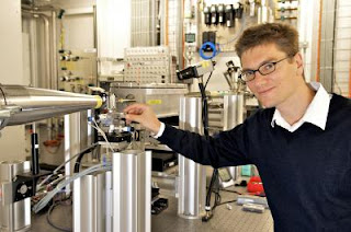
UBC President Stephen Toope and Max Planck Society President Peter Gruss were joined in Munich today by Thomas Marr, Germany's Minister-Counsellor of Commercial and Economic Affairs, for the signing of a memorandum of understanding (MOU) that will establish the Max Planck-UBC Centre for Quantum Materials.

The agreement also commits both institutions to conducting joint research projects in Canada and Germany, and to increasing scholarly exchanges.

"Today's agreement represents a joining of great strengths within both the Max Plank Society and UBC and will provide the underpinning for future research in advanced materials science," said Prof. Toope. "The knowledge and discoveries generated from these collaborations will profoundly change the lives of present and future generations."


The Max Planck-UBC Centre for Quantum Materials is only the third Max Planck Center to be established. The others are the Indo Max Planck Center for Computer Science in India and the CSIC-MPG Research Unit in Spain, which focuses on early European culture and religion. The first and only Max Planck Institute in North America is in Florida with Florida Atlantic University and is currently under construction.
UBC President Stephen Toope, Max Planck President Peter Gruss and UBC Vice President Research and International John Hepburn

(l to r) UBC President Stephen Toope, Max Planck President Peter Gruss and UBC Vice President Research and International John Hepburn at the Memorandum of Understanding signatory ceremony on Oct. 4, 2010. (Click on image to download high-resolution version
Today's MOU signing also marks the start of the Max Planck Society-UBC "Summer School" on Quantum Materials involving five lecturers and 10 graduate students and post-doctoral fellows from UBC and a similar number of participants from Germany.

Established in 1948, the Max Planck Society for the Advancement of Science is a non-governmental,
non-profit society that funds 80 institutes and research facilities in Germany and establishes strategic research partnerships with institutions around the world. Scientists from the society ¬– and its precursor, the Kaiser-Wilhelm-Society – have earned 32 Nobel prizes since 1914.

UBC is world renowned for research excellence in quantum materials – including superconductors – with potential applications in lossless power lines, vast improvements in computers and wireless communications, new advances in solar and fuel cells and a new class of medical electronic devices to aid diagnosis and treatment. To date, four Canada Research Chairs (CRC) in the area of condensed matter physics have been awarded to researchers at UBC, more than any other university in the country.

UBC principal investigators to lead research groups in the new Max Planck-UBC Centre include four CRC's and five Fellows of the Royal Society of Canada ¬¬– two of whom are also fellows of the Royal Society of London. In addition, three of the researchers are among the 100 most cited physicists in the world. They will be led by Prof. George Sawatzky, Canada Research Chair in Physics and Chemistry of Nano-structured Materials.

"The partnership with Max Planck is a testament to the caliber of research conducted here, and our researchers enjoy reputations as some of the most internationally collaborative in the world," said John Hepburn, UBC Vice President Research and International, who added that 46 per cent of UBC research is published jointly with colleagues outside Canada.

"Our interdisciplinary research strengths are further complemented by state-of-the-art facilities such as UBC's Advanced Materials and Process Engineering Laboratory, our vicinity to TRIUMF, Canada's National Laboratory for Particle and Nuclear Physics, and priority access to the Canadian Light Source Synchrotron."

Over the past 50 years, engineers have succeeded in developing smaller combinations of semiconductors, insulators and metals arranged to function as electronic devices while maintaining their fundamental electronic properties. Scientists at the forefront of advanced materials research are investigating the dramatic changes in properties that occur when such devices dive below current size limitations. ###

Contact: Brian Lin brian.lin@ubc.ca 604-822-2234 University of British Columbia

Saturday, October 23, 2010

Catalyst sandwich

Synthetic PCR mimic could lead to highly sensitive medical, environmental diagnostics

Northwestern University researchers have taken another step towards realizing a new class of polymerase chain reaction (PCR) enzyme mimics, opening the door for the development of highly sensitive chemical detection systems that go beyond nucleic acid targets.

The blueprint for building synthetic structures to detect and signal the presence of targets such as small molecule medical analytes (signalers of disease or bodily malfunction, such as neurotransmitters) and environmental hazards, such as TNT, to name just a few, is inspired by biology and its allosteric enzymes. The method also could be useful in catalysis and the production of polymers, including plastics.

The work, which promises higher sensitivity than that of current detection tools, was published Oct. 1 by the journal Science.

Chad Mirkin"PCR -- the backbone of the biodiagnostics industry -- is an enzyme that binds to a nucleic acid and changes shape, turning on a catalyst that makes copies of the nucleic acid for detection purposes," said Chad A. Mirkin, George B. Rathmann Professor of Chemistry in the Weinberg College of Arts and Sciences.

"What if you could do that for thousands of small molecules of interest?" he said.
"We'd like to be able to detect tiny amounts of targets important to medicine and the environment, opening avenues to new types of diagnostic tools, just as PCR did for the modern fields of medical diagnostics and forensics. Our new catalysts could make that possible."

Mirkin led a team of chemists who built a synthetic structure that, much like the layers of an Oreo cookie, sandwiches the catalyst between two chemically inert layers. This triple-layer architecture allows the use of any catalyst as it will be kept inactive, or in an "off" state, until triggered by a specific small molecule.

The enzyme mimic behaves like allosteric enzymes found in nature, catalysts that change shape to carry out their functions. (Hemoglobin is an example of an allosteric enzyme.) When the mimic reacts with a specific small molecule, the triple-layer structure changes shape and opens, exposing the catalyst. The resulting catalytic reaction signals the presence of the small molecule target, much like PCR amplifies a single piece of DNA.

"One of our challenges as synthetic chemists has been learning to synthesize structures inspired by biology but that have nothing to do with biology other than the fact we'd like such complex functions realized in man-made systems," said Mirkin, also director of Northwestern's International Institute for Nanotechnology.

In the work reported in Science, the researchers use an aluminum salen complex as the catalyst in the three-layer structure. The addition of chloride (the reduced form of chlorine) triggers the catalyst and starts the polymerization process. (Chloride ion binds at an allosteric binding site, distant from the active or catalytic site.) The addition of an agent that removes the chloride stops the process, but the chloride can be added back to start it again. ###

The title of the paper is "Allosteric Supramolecular Triple-Layer Catalysts." In addition to Mirkin, other authors of the paper are Hyo Jae Yoon, Junpei Kuwabara and Jun-Hyun Kim, all from Northwestern.

Contact: Megan Fellman fellman@northwestern.edu 847-491-3115 Northwestern University

Friday, October 22, 2010

Researcher at Childrens Hospital LA discovers way to overcome radiation resistance in leukemia

Radiation-resistant leukemia cells can be killed by radiation after inhibition of a molecular target by a rationally designed new drug.

LOS ANGELES (September 29, 2010) – A team of researchers lead by Fatih M. Uckun, MD, PhD, of The Saban Research Institute of Childrens Hospital Los Angeles has determined that radiation resistance in leukemia can be overcome by selectively attacking a molecular target known as SYK tyrosine kinase.

B-lineage acute lymphoblastic leukemia (ALL) is the most common cancer occurring in children and adolescents. Despite having received intensive chemotherapy, some patients have recurring disease, known as relapse. For these individuals, the prospect of long-term survival is poor.

The standard approach to treating relapsed patients has been additional chemotherapy to achieve a second remission followed by very intensive treatment that could include "supralethal" chemotherapy, total-body irradiation (TBI), and hematopoietic stem cell transplantation. However, radiation resistance of leukemia cells hampers the success of these rigorous therapeutic approaches and results in poor survival.

Fatih Uckun, Children's Hospital Los Angeles

Caption: This is Fatih Uckun, M.D., Ph.D., of Childrens Hospital Los Angeles.

Credit: Courtesy of Dr Uckun. Usage Restrictions: None.
"We knew that we could kill radiation-resistant leukemia cells if we only knew what made them so resistant. So we set out to determine the mechanism," said Dr. Uckun, who is also professor of Research Pediatrics at the Keck School of Medicine at the University of Southern California. "Once we determined the mechanism, the next step was obvious -- to rationally design a drug that would take out that specific target."
Uckun's research team has now provided the first proof-of-principle that radiation resistance of an aggressive leukemia can indeed be overcome using this rationally-designed specific drug directed against the resistance machinery of leukemia cells.

"Radiation therapy was much more effective against leukemia in mice when it was combined with this new drug candidate that we named C-61," said Dr. Uckun. ###

The results of the study will be published in the October 2010 issue of Radiation Research, the official journal of the Radiation Research Society.

The Saban Research Institute at Childrens Hospital Los Angeles is among the largest and most productive pediatric research facilities in the United States, with 100 investigators at work on 186 laboratory studies, clinical trials and community-based research and health services. The Saban Research Institute is ranked eighth in National Institutes of Health funding among children's hospitals in the United States.

Founded in 1901, Childrens Hospital Los Angeles is one of the nation's leading children's hospitals and is acknowledged worldwide for its leadership in pediatric and adolescent health. Childrens Hospital Los Angeles is one of only seven children's hospitals in the nation – and the only children's hospital on the West Coast – ranked for two consecutive years in all 10 pediatric specialties in the U.S. News & World Report rankings and named to the magazine's "Honor Roll" of children's hospitals.

Childrens Hospital Los Angeles is a premier teaching hospital and has been affiliated with the Keck School of Medicine of the University of Southern California since 1932.

Reference: F. M. Uckun, I. Dibirdik, S. Qazi (2010) Augmentation of the Antileukemia Potency of Total-Body Irradiation (TBI) by a Novel P-site Inhibitor of Spleen Tyrosine Kinase (SYK). Radiation Research: October 2010, Vol. 174, No. 4, pp. 526-531.

Contact: Ellin Kavanagh ekavanagh@chla.usc.edu 323-361-8505 Children's Hospital Los Angeles

Thursday, October 21, 2010

Growing nanowires horizontally yields new benefit: 'nano-LEDs'

While refining their novel method for making nanoscale wires, chemists at the National Institute of Standards and Technology (NIST) discovered an unexpected bonus—a new way to create nanowires that produce light similar to that from light-emitting diodes (LEDs). These "nano-LEDs" may one day have their light-emission abilities put to work serving miniature devices such as nanogenerators or lab-on-a-chip systems.

Nanowires typically are "grown" by the controlled deposition of molecules—zinc oxide, for example—from a gas onto a base material, a process called chemical vapor deposition (CVD). Most CVD techniques form nanowires that rise vertically from the surface like brush bristles. Because the wire only contacts the substrate at one end, it tends not to share characteristics with the substrate material—a less-than-preferred trait because the exact composition of the nanowire will then be hard to define.

Nano LEDs

Growing Nanowires Horizontally Yields New Benefit: 'Nano-LEDs' Caption: This is an optical microscope image of "nano LEDs" emitting light.

Credit: NIST. Usage Restrictions: None.

Nano LEDs

Caption: This graphic illustrates a single row of nanowires (cylinders with red tops) with fin-shaped nanowalls extending outward.

Credit: NIST. Usage Restrictions: None.
Vertical growth also produces a dense forest of nanowires, making it difficult to find and re-position individual wires of superior quality. To remedy these shortcomings, NIST chemists Babak Nikoobakht and Andrew Herzing developed a "surface-directed" method for growing nanowires horizontally across the substrate (see "NIST Demos Industrial-Grade Nanowire Device Fabrication" NIST Tech Beat, Oct. 25, 2007, at www.nist.gov/public_affairs/techbeat/nanowire).

Like many vertical growth CVD methods, the NIST fabrication technique uses gold as a catalyst for crystal formation. The difference is that the gold deposited in the NIST method is heated to 900 degrees Celsius (1,652 degrees Fahrenheit), converting it to a nanoparticle that serves as growth site and medium for the crystallization of zinc oxide molecules. As the zinc oxide nanocrystal grows, it pushes the gold nanoparticle along the surface of the substrate (in this experiment, gallium nitride) to form a nanowire that grows horizontally across the substrate and so exhibits properties strongly influenced by its base material.

In recent work published in ACS Nano,* Nikoobakht and Herzing increased the thickness of the gold catalyst nanoparticle from less than 8 nanometers to approximately 20 nanometers.
The change resulted in nanowires that grew a secondary structure, a shark-like "dorsal fin" (referred to as a "nanowall") where the zinc oxide portion is electron-rich and the gallium nitride portion is electron-poor. The interface between these two materials—known as a p-n heterojunction—allows electrons to flow across it when the nanowire-nanowall combination was charged with electricity. In turn, the movement of electrons produced light and led the researchers to dub it a "nano LED."

Unlike previous techniques for producing heterojunctions, the NIST "surface-directed" fabrication method makes it easy to locate individual heterojunctions on the surface. This feature is especially useful when a large number of heterojunctions must be grouped in an array so that they can be electrically charged as a light-emitting unit.

Transmission electron microscope (TEM) examination of the zinc oxide-gallium nitride nanowires and nanowalls revealed few structural defects in the nanowires and very distinct p-n heterojunctions in the nanowalls, both affirmations of the effectiveness of the NIST "surface directed" fabrication method.

Nikoobakht and Herzing hope to improve the nano LEDs in future experiments using better geometry and material designs, and then apply them in the development of light sources and detectors useful in photonic devices or lab-on-a-chip platforms. ###

* B. Nikkoobakht and A. Herzing. Formation of planar arrays of one-dimensional p-n heterojunctions using surface-directed growth of nanowires and nanowalls. ACS Nano. Published online Sept. 15, 2010.

Contact: Michael E. Newman michael.newman@nist.gov 301-975-3025 National Institute of Standards and Technology (NIST)

Wednesday, October 20, 2010

A shot to the heart: Nanoneedle delivers quantum dots to cell nucleus

CHAMPAIGN, Ill. — Getting an inside look at the center of a cell can be as easy as a needle prick, thanks to University of Illinois researchers who have developed a tiny needle to deliver a shot right to a cell's nucleus.

Understanding the processes inside the nucleus of a cell, which houses DNA and is the site for transcribing genes, could lead to greater comprehension of genetics and the factors that regulate expression. Scientists have used proteins or dyes to track activity in the nucleus, but those can be large and tend to be sensitive to light, making them hard to use with simple microscopy techniques.

Researchers have been exploring a class of nanoparticles called quantum dots, tiny specks of semiconductor material only a few molecules big that can be used to monitor microscopic processes and cellular conditions. Quantum dots offer the advantages of small size, bright fluorescence for easy tracking, and excellent stability in light.

Nanoneedle Delivers Quantum Dots to Nucleus

Caption: University of Illinois researchers developed a nanoneedle that releases quantum dots directly into the nucleus of a living cell when a small electrical charge is applied. The quantum dots are tracked to gain information about conditions inside the nucleus.

Credit: Min-Feng Yu, University of Illinois. Usage Restrictions: None.

Professor Min-Feng Yu, University of Illinois

Caption: Min-Feng Yu, professor of mechanical science and engineering at the University of Illinois.

Credit: L. Brian Stauffer. Usage Restrictions: None.
"Lots of people rely on quantum dots to monitor biological processes and gain information about the cellular environment. But getting quantum dots into a cell for advanced applications is a problem," said professor Min-Feng Yu, a professor of mechanical science and engineering.

Getting any type of molecule into the nucleus is even trickier, because it's surrounded by an additional membrane that prevents most molecules in the cell from entering.

Yu worked with fellow mechanical science and engineering professor Ning Wang and postdoctoral researcher Kyungsuk Yum to develop a nanoneedle that also served as an electrode that could deliver quantum dots directly into the nucleus of a cell – specifically to a pinpointed location within the nucleus. The researchers can then learn a lot about the physical conditions inside the nucleus by monitoring the quantum dots with a standard fluorescent microscope.

"This technique allows us to physically access the internal environment inside a cell," Yu said. "It's almost like a surgical tool that allows us to 'operate' inside the cell."

The group coated a single nanotube, only 50 nanometers wide, with a very thin layer of gold, creating a nanoscale electrode probe. They then loaded the needle with quantum dots. A small electrical charge releases the quantum dots from the needle. This provides a level of control not achievable by other molecular delivery methods, which involve gradual diffusion throughout the cell and into the nucleus.
"Now we can use electrical potential to control the release of the molecules attached on the probe," Yu said. "We can insert the nanoneedle in a specific location and wait for a specific point in a biologic process, and then release the quantum dots. Previous techniques cannot do that."

Because the needle is so small, it can pierce a cell with minimal disruption, while other injection techniques can be very damaging to a cell. Researchers also can use this technique to accurately deliver the quantum dots to a very specific target to study activity in certain regions of the nucleus, or potentially other cellular organelles.

"Location is very important in cellular functions," Wang said. "Using the nanoneedle approach you can get to a very specific location within the nucleus. That's a key advantage of this method."

The new technique opens up new avenues for study. The team hopes to continue to refine the nanoneedle, both as an electrode and as a molecular delivery system.

They hope to explore using the needle to deliver other types of molecules as well – DNA fragments, proteins, enzymes and others – that could be used to study a myriad of cellular processes.

"It's an all-in-one tool," Wang said. "There are three main types of processes in the cell: chemical, electrical, and mechanical. This has all three: It's a mechanical probe, an electrode, and a chemical delivery system."

The team's findings will appear in the Oct. 4 edition of the journal Small. The National Institutes of Health and the National Science Foundation supported this work. ###

Editor's note: To contact Min-Feng Yu, call 217-333-9246; e-mail mfyu@illinois.edu. To contact Ning Wang, call 217-265-0913; e-mail nwangrw@illinois.edu.

Contact: Liz Ahlberg eahlberg@illinois.edu 217-244-1073 University of Illinois at Urbana-Champaign

Tuesday, October 19, 2010

Rethinking renewables: A new approach to energy storage for wind and solar

Rensselaer Polytechnic Institute researchers win $2 million NSF grant to develop capacitive energy storage system for renewable power source

Troy, N.Y. – Researchers at Rensselaer Polytechnic Institute are leading a new $2 million study to help overcome a key bottleneck slowing the proliferation of large-scale wind and solar power generation.

Funded by a $2 million grant from the U.S. National Science Foundation, the four-year study aims to develop novel ceramic materials for use in a new approach to energy storage. Rather than batteries, the researchers will develop nanostructured capacitors to store energy that is generated and converted by wind turbines and solar panels. With an extremely high power density and the ability to very quickly charge and discharge, these nanoengineered capacitors could be a game-changer impacting a wide range of applications, from energy production to electronics to national defense.

Doug Chrisey

Doug Chrisey
"The transformative nature of capacitive energy storage – a totally new approach to energy storage – will have a tremendous impact on the increased use and efficiency of wind and solar power, as well as conventional coal, nuclear, and hydroelectric generation," said Doug Chrisey, professor in the Department of Materials Science and Engineering at Rensselaer, who is leading the study.
"Our proposed capacitors will be smaller, lighter, and more efficient than today's batteries, and with no moving parts the capacitors should last forever. Everyone is looking for a truly innovative material to help meet future energy requirements, and we're confident that our novel ceramic will help advance that conversation."

The grant was awarded through the NSF Emerging Frontiers in Research and Innovation (EFRI) Program, overseen by the NSF Engineering Directorate, which identifies and supports interdisciplinary initiatives at the emerging frontier of engineering research and education. For the study, Chrisey is partnering with renowned glass expert and Rensselaer Professor Minoru Tomozawa, along with nanoscientist and University of Puerto Rico, Río Piedras Professor Ram S. Katiyar.

Unlike a battery, which supplies a continuous level of low power for long periods of time, a capacitor moves large amounts of power very quickly. The ideal solution for electrical energy storage, Chrisey said, will allow fast energy storage and discharge in as small a volume or mass as possible. To achieve this, the researchers will develop a nanostructured capacitor comprising extremely thin layers of a novel composite. The composite is a mix of ferroelectric nanopowder and low-melting, alkali-free glass. The result is a capacitor that can withstand high electric fields and maintain an extremely high dielectric constant – two critical metrics for measuring the effectiveness of energy storage materials.

In addition to optimizing and perfecting the composition of the novel ceramic material, Chrisey and team are tasked with developing new processes to make the material easily and in large quantities.

"Creating a novel ceramic material and developing a cost-effective, scalable method to achieve large-capacitive energy storage could be a big boost to our national economy and increase our global competitiveness," Chrisey said. "What we need is an entirely new approach to energy storage, and we think ferroelectric glass composites could be the answer." ###

Contact: Michael Mullaney mullam@rpi.edu 518-276-6161 Rensselaer Polytechnic Institute

Sunday, October 17, 2010

Nanobiotechnology experts join forces to improve TB testing

Two UK companies have been awarded joint funding for a research project that could see significant advances in the quest to aid detection and eradication of Tuberculosis (TB), across the world.

The National Physical Laboratory (NPL) and Orla Protein Technologies (Orla) have been awarded £91,000 by the Technology Strategy Board to investigate improved methods for the detection of TB.

The project, which begins in this month, involves a combination of cutting edge technologies and expertise based here in the UK, including areas of molecular and biological diagnostics (Orla), and measurement science and infectious diseases (NPL).

Mycobacterium tuberculosis (MTB) is a pathogenic bacterial species in the genus Mycobacterium and the causative agent of almost all cases if tuberculosis.

Nanobiotechnology experts join forces to improve TB testingMore than five thousand people die every day from TB, largely in the developing world. TB is one of the major lethal factors among AIDS patients. Largely, TB affects the developing world where the situation is worsened with the infection becoming one of the main lethal factors among HIV-infected individuals.
Current methods of TB detection suffer from a need for large sample volumes, long preparation times and different results from different patient groups. This has led to a demand for more sensitive and rapid approaches to be developed.

The Consortium aims to meet this demand, by producing systems which dramatically advance current methods; helping to improve the sensitivity, specificity, cost and speed of results.

Max Ryadnov, Project Leader at NPL, said: "The main objective of the project is to demonstrate the possibility of detecting MTB quickly and cost effectively in both clinical and near-patient settings. Such capability is a Holy Grail of modern diagnostics of MTB and would significantly impact on the UK and global healthcare markets."

The study will make use of techniques developed at the National Physical Laboratory for the detection of MTB antigens - biomarkers which indicate disease – to rapidly assess the presence of the MTB in a sample. These techniques are empowered by a unique technology developed by Orla PT allowing the fabrication of protein patterned surfaces responsive to MTB biomarkers thereby making the manufacture and use of biomarker detection dramatically simpler"

Dale Athey, Chief Executive at Orla, said: "The development of such procedures will help to substantially improve health systems in resource-limiting settings, particularly in HIV-infected TB cases, where sensitivity remains well below confidence limits for all MTB tests.

"We hope the project will allow us to significantly improve consistency and enhanced sensitivity for cost-effective, easy to use point-of-care-solutions for the detection and eradication of MTB."

The project team will also work closely with colleagues in the Health Protection Agency for advice on microbiology, and to arrange testing in a clinical environment. ###

For more information on Orla Protein Technologies, please contact Anna at Goulding Public Relations on 0191 209 2795 / 07957639486 or by emailing anna@gouldingpr.com

NOTES TO EDITORS

About Orla Protein Technologies Ltd

Orla Protein Technologies Ltd is a nano-biotechnology company focused on developing high performance biosurfaces which have applications in cell culture, Life Science tools and Reagents, and Diagnostics. The core technology was developed by Professor Jeremy Lakey, Professor of Structural Biochemistry at Newcastle University. Orla was founded in 2002 and received seed investment from NEL Fund Managers Ltd in 2003. For more information see www.orlaproteins.com

About The National Physical Laboratory

The National Physical Laboratory (NPL) is one of the UK's leading science and research facilities. It is a world-leading centre of excellence in developing and applying the most accurate standards, science and technology available.

NPL occupies a unique position as the UK's National Measurement Institute and sits at the intersection between scientific discovery and real world application. Its expertise and original research have underpinned quality of life, innovation and competitiveness for UK citizens and business for more than a century: NPL provides companies with access to world-leading support and technical expertise, inspiring the absolute confidence required to realise competitive advantage from new materials, techniques and technologies;

NPL expertise and services are crucial in a wide range of social applications - helping to save lives, protect the environment and enable citizens to feel safe and secure. Support in areas such as the development of advanced medical treatments and environmental monitoring helps secure a better quality of life for all;

NPL develops and maintains the nation's primary measurement standards, supporting an infrastructure of traceable measurement throughout the UK and the world, to ensure accuracy and consistency. www.npl.co.uk

About the Technology Strategy Board The Technology Strategy Board is a business-led executive non-departmental public body, established by the government. Its role is to promote and support research into, and development and exploitation of, technology and innovation for the benefit of UK business, in order to increase economic growth and improve the quality of life. It is sponsored by the Department for Business, Innovation and Skills (BIS). For more information please visit www.innovateuk.org.

Contact: David Lewis david@proofcommunication.com 084-568-01865 National Physical Laboratory

Saturday, October 16, 2010

Single electron reader opens path for quantum computing

Researchers develop key building block needed to make a quantum computer using silicon

A team led by engineers and physicists at the University of New South Wales (UNSW) in Sydney, Australia, have developed one of the key building blocks needed to make a quantum computer using silicon: a "single electron reader". Their work was published today in Nature.

Quantum computers promise exponential increases in processing speed over today's computers through their use of the "spin", or magnetic orientation, of individual electrons to represent data in their calculations.

In order to employ electron spin, the quantum computer needs both a way of changing the spin state (write) and of measuring that change (read) to form a qubit – the equivalent of the bits in a conventional computer.

Dr Andrea Morello

Dr Andrea Morello. Program Manager Quantum Measurement & Control Chip University of New South Wales.
In creating the single electron reader, a team of engineers and physicists led by Dr Andrea Morello and Professor Andrew Dzurak, of the School of Electrical Engineering and Telecommunications at UNSW, has for the first time made possible the measurement of the spin of one electron in silicon in a single shot experiment. The team also includes researchers from the University of Melbourne and Aalto University in Finland.

"Our device detects the spin state of a single electron in a single phosphorus atom implanted in a block of silicon. The spin state of the electron controls the flow of electrons in a nearby circuit," said Dr Morello, the lead author of the paper, Single-shot readout of an electron spin in silicon.
"Until this experiment, no-one had actually measured the spin of a single electron in silicon in a single-shot experiment."

By using silicon—the foundation material of conventional computers—rather than light or the esoteric materials and approaches being pursued by other researchers, the device opens the way to constructing a simpler quantum computer, scalable and amenable to mass-production.

The team has built on a body of research that has put Australia at forefront of the race to construct a working quantum computer. In 1998 Bruce Kane, then at UNSW, outlined in Nature the concept for a silicon-based quantum computer, in which the qubits are defined by single phosphorus atoms in an otherwise ultra-pure silicon chip. The new device brings his vision closer.

"We expect quantum computers will be able to perform certain tasks much faster than normal computers, such as searching databases, modelling complex molecules or developing new drugs," says co-author Prof Andrew Dzurak. "They could also crack most modern forms of encryption."

"After a decade of work trying to build this type of single atom qubit device, this is a very special moment."

Now the team has created a single electron reader, they are working to quickly complete a single electron writer and combine the two. Then they will combine pairs of these devices to create a 2-bit logic gate – the basic processing unit of a quantum computer. ###

The research team is part of the Australian Research Council (ARC) Centre of Excellence for Quantum Computer Technology, which is headquartered at UNSW. The team is led by Professor Dzurak and Dr Morello, with Mr Jarryd Pla and Dr Floris Zwanenburg as key supporting experimentalists. The paper's co-authors include Prof David Jamieson from the University of Melbourne; Dr Bob Clark, Australia's Chief Defence Scientist, and 10 other researchers from UNSW, The University of Melbourne, and Finland's Aalto University.

The research was funded by: the Australian, US, and NSW governments; UNSW; and the University of Melbourne.

Contact: Peter Trute p.trute@unsw.edu.au 61-293-851-933 University of New South Wales

Friday, October 15, 2010

New computer-tomography method visualizes nano-structure of bones

Advanced imaging for osteoporosis research and materials science.

A novel nano-tomography method developed by a team of researchers from the Technische Universitaet Muenchen, the Paul Scherrer Institute and the ETH-Zurich opens the door to computed tomography examinations of minute structures at nanometer resolutions. Three-dimensional detailed imaging of fragile bone structures becomes possible. Their first nano-CT images will be published in Nature on Sept. 23, 2010. This new technique will facilitate advances in both life sciences and materials sciences.

Osteoporosis, a medical condition in which bones become brittle and fragile from a loss of density, is among the most common diseases in aging bones: In Germany around a quarter of the population aged over 50 is affected. Patients' bone material shrinks rapidly, leading to a significantly increased risk of fracture.

Franz Pfeiffer, Technische Universitaet Muenchen

Caption: This is Franz Pfeiffer in front of the experimental setup he developed with his team at the Swiss Light Source of the Paul Scherrer Institute, where the new nano-CT method was implemented.

Credit: Markus Fischer, PSI. Usage Restrictions: None.
In clinical research to date, osteoporosis is diagnosed almost exclusively by establishing an overall reduction in bone density. This approach, however, gives little information about the associated, and equally important, local structure and bone density changes. Franz Pfeiffer, professor for Biomedical Physics at the Technische Universitaet Muenchen (TUM) and head of the research team, has resolved the dilemma: "With our newly developed nano-CT method it is now possible to visualize the bone structure and density changes at high resolutions and in 3D. This enables us to do research on structural changes related to osteoporosis on a nanoscale and thus develop better therapeutic approaches."
During development, Pfeiffer's team built on X-ray computed tomography (CT). The principle is well established – CT scanners are used every day in hospitals and medical practices for the diagnostic screening of the human body. In the process the human body is X-rayed while a detector records from different angles how much radiation is being absorbed. In principle it is nothing more than taking multiple X-ray pictures from various directions. A number of such pictures are then used to generate digital 3D images of the body's interior using image processing.

The newly developed method measures not only the overall beam intensity absorbed by the object under examination at each angle, but also those parts of the X-ray beam that are deflected in different directions – "diffracted" in the language of physics. Such a diffraction pattern is generated for every point in the sample. This supplies additional information about the exact nanostructure, as X-ray radiation is particularly sensitive to the tiniest of structural changes. "Because we have to take and process so many individual pictures with extreme precision, it was particularly important during the implementation of the method to use high-brilliance X-ray radiation and fast, low-noise pixel detectors – both available at the Swiss Light Source (SLS)," says Oliver Bunk, who was responsible for the requisite experimental setup at the PSI synchrotron facilities in Switzerland.

The diffraction patterns are then processed using an algorithm developed by the team. TUM researcher Martin Dierolf, lead author of the Nature article, explains: "We developed an image reconstruction algorithm that generates a high-resolution, three-dimensional image of the sample using over one hundred thousand diffraction patterns. This algorithm takes into account not only classical X-ray absorption, but also the significantly more sensitive phase shift of the X-rays." A showcase example of the new technique was the examination of a 25-micrometer, superfine bone specimen of a laboratory mouse – with surprisingly exact results. The so-called phase contrast CT pictures show even smallest variations in the specimen's bone density with extremely high precision: Cross-sections of cavities where bone cells reside and their roughly 100 nanometer-fine interconnection network are clearly visible.

"Although the new nano-CT procedure does not achieve the spatial resolution currently available in electron microscopy, it can – because of the high penetration of X-rays – generate three-dimensional tomography images of bone samples," comments Roger Wepf, director of the Electron Microscopy Center of the ETH Zurich (EMEZ). "Furthermore, the new nano-CT procedure stands out with its high precision bone density measurement capacity, which is particularly important in bone research." This method will open the door to more precise studies on the early phase of osteoporosis, in particular, and evaluation of the therapeutic outcomes of various treatments in clinical studies.

The new technique is also very interesting for non-medical applications: Further fields of application include the development of new materials in materials science or in the characterization of semiconductor components. Ultimately, the nano-CT procedure may also be transferred to novel, laser-based X-ray sources, such as the ones currently under development at the Cluster of Excellence "Munich-Centre for Advanced Photonics" (MAP) and at the recently approved large-scale research project "Centre for Advanced Laser Applications" (CALA) on the TUM-Campus Garching near Munich. ###

Contact: Dr. Andreas Battenberg battenberg@zv.tum.de 49-892-891-0510 Technische Universitaet Muenchen

Thursday, October 14, 2010

Nanocatalyst is a gas

Rice U. formula could make fuel production better, greener.

HOUSTON – (Sept. 20, 2010) – A nanoparticle-based catalyst developed at Rice University may give that tiger in your tank a little more roar.

A new paper in the Journal of the American Chemical Society details a process by Rice Professor Michael Wong and his colleagues that should help oil refineries make the process of manufacturing gasoline more efficient and better for the environment.

In addition, Wong said, it could produce higher-octane gasoline and save money for an industry in which a penny here and a penny there add millions to the bottom line.

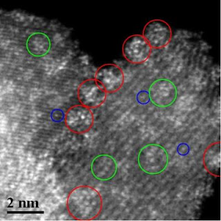
Wong's team at Rice, in collaboration with labs at Lehigh University, the Centre for Research and Technology Hellas and the DCG Partnership of Texas, reported this month that sub-nanometer clusters of tungsten oxide lying on top of zirconium oxide are a highly efficient catalyst that turns straight-line molecules of n-pentane, one of many hydrocarbons in gasoline, into better-burning branched n-pentane.

Tungsten Oxide Nanoparticles

Caption: This is an atomic-level image of tungsten oxide nanoparticles (green circles) on zirconia support. The other circles show the less-active forms of tungsten oxide.

Credit: Wu Zhou/Lehigh University. Usage Restrictions: None.
While the catalytic capabilities of tungsten oxide have long been known, it takes nanotechnology to maximize their potential, said Wong, a Rice professor of chemical and biomolecular engineering and of chemistry.

After the initial separation of crude oil into its basic components -- including gasoline, kerosene, heating oil, lubricants and other products -- refineries "crack" (by heating) heavier byproducts into molecules with fewer carbon atoms that can also be made into gasoline. Catalysis, a chemical process, further refines these hydrocarbons.

That's where Wong's discovery comes in. Refineries strive to make better catalysts, he said, although "compared with the academic world, industry hasn't done much in terms of new synthesis techniques,
new microscopy, new biology, even new physics. But these are things we understand in the context of nanotechnology.

"We have a way to make a better catalyst that will improve the fuels they make right now. At the same time, a lot of existing chemical processes are wasteful in terms of solvents, precursors and energy. Improving a catalyst can also make the chemical process more environmentally friendly. Knock those things out, and they gain efficiencies and save money."

Wong and his team have worked for several years to find the proper mix of active tungsten oxide nanoparticles and inert zirconia. The key is to disperse nanoparticles on the zirconia support structure at the right surface coverage. "It's the Goldilocks theory – not too much, not too little, but just right," he said. "We want to maximize the amount of these nanoparticles on the support without letting them touch.

"If we hit that sweet spot, we can see an increase of about five times in the efficiency of the catalyst. But this was very difficult to do."

No wonder. The team had to find the right chemistry, at the right high temperature, to attach particles a billionth of a meter wide to grains of zirconium oxide powder. With the right mix, the particles react with straight n-pentane molecules, rearranging their five carbon and 12 hydrogen atoms in a process called isomerization.

Now that the catalyst formula is known, making the catalyst should be straightforward for industry. "Because we're not developing a whole new process – just a component of it – refineries should be able to plug this into their systems without much disruption," Wong said.

Maximizing gasoline is important as the world develops new sources of energy, he said. "There's a lot of talk about biofuels as a significant contributor in the future, but we need a bridge to get there. Our discovery could help by stretching current fuel-production capabilities." ###

Co-authors of the paper are Nikolaos Soultanidis, a Rice chemical engineering graduate student in Wong's lab; Israel Wachs, Wu Zhou and Christopher Kiely of Lehigh University; Antonis Psarras and Eleni Iliopoulou of the Centre for Research and Technology Hellas; and Alejandro Gonzalez of the DCG Partnership, Pearland, Texas.

The National Science Foundation's Nanoscale Interdisciplinary Research Team Program supported the project, with additional support from SABIC Americas and 3M.

Contact: Mike Williams mikewilliams@rice.edu 713-348-6728 Rice University

Wednesday, October 13, 2010

Research team assesses environmental impact of organic solar cells

Study evaluates the manufacture, material use and performance of solar cell technology

Solar energy could be a central alternative to petroleum-based energy production. However, current solar-cell technology often does not produce the same energy yield and is more expensive to mass-produce. In addition, information on the total effect of solar energy production on the environment is incomplete, experts say.

To better understand the energy and environmental benefits and detriments of solar power, a research team from Rochester Institute of Technology has conducted one of the first life-cycle assessments of organic solar cells. The study found that the embodied energy — or the total energy required to make a product — is less for organic solar cells compared with conventional inorganic devices.

Annick Anctil

Annick Anctil, a fourth-year doctoral student in sustainability, conducts experiments on different varieties of solar cells in RIT's NanoPower Research Labs. Through a grant from the U.S. Department of Energy, Anctil conducted one of the first life-cycle assessments of organic solar cells.

Photo by Laura W. Nelson.
"This analysis provides a comprehensive assessment of how much energy it takes to manufacture an organic solar cell, which has a significant impact on both the cost and environmental impact of the technology," says Brian Landi, assistant professor of chemical engineering at RIT and a faculty advisor on the project

"Organic solar cells are flexible and lightweight, and they have the promise of low-cost solution processing, which can have advantages for manufacturing over previous-generation technologies that primarily use inorganic semiconductor materials," adds Annick Anctil, lead researcher on the study and a fourth-year doctoral candidate in RIT's doctoral program in sustainability.
"However, previous assessments of the energy and environmental impact of the technology have been incomplete and a broader analysis is needed to better evaluate the overall effect of production and use."

The study sought to calculate the total energy use and environmental impact of the material collection, fabrication, mass production and use of organic solar cells through a comprehensive life-cycle assessment of the technology.

According to Anctil, previous life-cycle assessments had not included a component-by-component breakdown of the individual materials present in an organic solar cell or a calculation of the total energy payback of the device, which is defined as the energy produced from its use versus the energy needed to manufacture the cell.

The team found that when compared to inorganic cells, the energy payback time for organic solar cells was lower. Ongoing studies to verify the device stability are still warranted, however.

"The data produced will help designers and potential manufacturers better assess how to use and improve the technology and analyze its feasibility versus other solar and alternative-energy technologies," adds Landi. ###

The team presented the results at the Institute for Electrical and Electronics Engineers 2010 Photovoltaic Specialists Conference. Anctil, who won a student award at the conference for best research, hopes to further analyze the environmental impacts of solar cell development with additional life-cycle assessments of other types of solar cell technology.

The study was funded through the United States Department of Energy and also included researchers from RIT's Golisano Institute for Sustainability and NanoPower Research Labs.

Contact: William Dube wjduns@rit.edu 585-475-2816 Rochester Institute of Technology