Saturday, July 31, 2010

Transformation optics make a U-turn for the better

Powerful new microscopes able to resolve DNA molecules with visible light, superfast computers that use light rather than electronic signals to process information, and Harry Potteresque invisibility cloaks are just some of the many thrilling promises of transformation optics. In this burgeoning field of science, light waves can be controlled at all lengths of scale through the unique structuring of metamaterials, composites typically made from metals and dielectrics - insulators that become polarized in the presence of an electromagnetic field. The idea is to transform the physical space through which light travels, sometimes referred to as "optical space," in a manner similar to the way in which outer space is transformed by the presence of a massive object under Einstein's relativity theory.

So far transformation optics have delivered only hints as to what the future might hold, with a major roadblock being how difficult it is to modify the physical properties of metamaterials at the nano or subwavelength scale, mainly because of the metals. Now, a team of researchers with the U.S. Department of Energy (DOE)'s Lawrence Berkeley National Laboratory (Berkeley Lab) and the University of California (UC) Berkeley have shown it might be possible to go around that metal roadblock.

180 Degree Bend

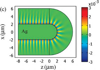
Caption: Field distribution after the transformation of a dielectric material shows the nearly perfect transmission of a light beam around a 180 degree bend.

Credit: (Image courtesy of Zhang group. Usage Restrictions: None.

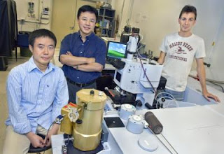
Xiang Zhang, Yongmin Liu and Thomas Zentgraf

Caption: Yongmin Liu (left) Xiang Zhang and Thomas Zentgraf used sophisticated compuer modeling to develop a "transformational plasmon optics" technique that may open the door to practical integrated, compact optical data-processing chips.

Credit: Photo by Roy Kaltschmidt, Berkeley Lab Public Affairs. Usage Restrictions: None.

Transformational Optics

Caption: Schematic on the left shows the scattering of surface plasmon polaritons (SPPs) on a metal-dielectric interface with a single protrusion. Schematic on right shows how SPP scattering is dramatically suppressed when the optical space around the protrusion is transformed.

Credit: Image courtesy of Zhang group. Usage Restrictions: None.
Using sophisticated computer simulations, they have demonstrated that with only moderate modifications of the dielectric component of a metamaterial, it should be possible to achieve practical transformation optics results. The key to success is the combination of transformation optics with another promising new field of science known as plasmonics.

A plasmon is an electronic surface wave that rolls through the sea of conduction electrons on a metal. Just as the energy in waves of light is carried in quantized particle-like units called photons, so, too, is plasmonic energy carried in quasi-particles called plasmons. Plasmons will interact strongly with photons at the interface of a metamaterial's metal and dielectric to form yet another quasi-particle called a surface plasmon polariton(SPP). Manipulation of these SPPs is at the heart of the astonishing optical properties of metamaterials.

The Berkeley Lab-UC Berkeley team, led by Xiang Zhang, a principal investigator with Berkeley Lab's Materials Sciences Division and director of UC Berkeley's Nano-scale Science and Engineering Center (SINAM), modeled what they have dubbed a "transformational plasmon optics" approach that involved manipulation of the dielectric material adjacent to a metal but not the metal itself. This novel approach was shown to make it possible for SPPs to travel across uneven and curved surfaces over a broad range of wavelengths without suffering significant scattering losses. Using this model, Zhang and his team then designed a plasmonic waveguide with a 180 degree bend that won't alter the energy or properties of a light beam as it makes the U-turn. They also designed a plasmonic version of a Luneburg lens, the ball-shaped lenses that can receive and resolve optical waves from multiple directions at once.

"Since the metal properties in our metamaterials are completely unaltered, our transformational plasmon optics methodology provides a practical way for routing light at very small scales," Zhang says. "Our findings reveal the power of the transformation optics technique to manipulate near-field optical waves, and we expect that many other intriguing plasmonic devices will be realized based on the methodology we have introduced."
Zhang is the corresponding author of a paper describing this research that appeared in the journal Nano Letters, titled "Transformational Plasmon Optics." Co-authoring the paper with Zhang were Yongmin Liu, Thomas Zentgraf and Guy Bartal.

Says Liu, who was the lead author of the paper and is a post-doctoral researcher in Zhang's UC Berkeley group, "In addition to the 180 degree plasmonic bend and the plasmonic Luneburg lens, our approach should also enable the design and production of beam splitters and shifters, and directional light emitters. The technique should also be applicable to the construction of integrated, compact optical data-processing chips."

Zhang and his research group have been at the forefront of transformation optics research since 2008 when they became the first group to fashion metamaterials that were able to bend light backwards, a property known as "negative refraction," which is unprecedented in nature. In 2009, he and his group created a "carpet cloak" from nanostructured silicon that concealed the presence of objects placed under it from optical detection.

For this latest work, Zhang and Liu with Zentgraf and Bartal departed from the traditional transformation optics focus on propagation waves and instead focused on the SPPs carried in near-field (subwavelength) region.

"The intensity of SPPs is maximal at the interface between a metal and a dielectric medium and exponentially decays away from the interface," says Zhang. "Since a significant portion of SPP energy is carried in the evanescent field outside the metal, that is, in the adjacent dielectric medium, we proposed to control SPPs by keeping the metal property fixed and only modifying the dielectric material based on the transformation optics technique."

Full-wave simulations of different transformed designs proved the proposed methodology by Zhang and his colleagues correct. It was furthermore demonstrated that if a prudent transformational plasmon optics scheme is taken the transformed dielectric materials can be isotropic and nonmagnetic, which further boosts the practicality of this approach. The demonstration of a 180 degree bend plasmonic bend with almost perfect transmission was especially significant.

"Plasmonic waveguides are one of the most important components/elements in integrated plasmonic devices," says Liu. "However, curvatures often lead to strong radiation loss that reduces the length for transferring an optical signal. Our 180 degree bend plasmonic bend is definitely important and will be useful in the future design of integrated plasmonic devices."

Compared with silicon-based photonic devices the use of plasmonics could help to further scale- down the total size of photonic devices and increase the interaction of light with certain materials, which should improve performance.

"We envision that the unique design flexibility of the transformational plasmon optics approach may open a new door to nano optics and photonic circuit design," Zhang says. ###

This research was supported by the U.S. Army Research Office and the National Science Foundation's Nano-scale Science and Engineering Center.

Berkeley Lab is a U.S. Department of Energy (DOE) national laboratory located in Berkeley, California. It conducts unclassified scientific research and is managed by the University of California for the DOE Office of Science. Visit our Website at: www.lbl.gov.

Contact: Lynn Yarris lcyarris@lbl.gov 510-486-5375 DOE/Lawrence Berkeley National Laboratory

Thursday, July 29, 2010

Nano-sized light mill drives micro-sized disk VIDEO

While those wonderful light sabers in the Star Wars films remain the figment of George Lucas' fertile imagination, light mills - rotary motors driven by light – that can power objects thousands of times greater in size are now fact. Researchers with the U.S. Department of Energy (DOE)'s Lawrence Berkeley National Laboratory and the University of California (UC) Berkeley have created the first nano-sized light mill motor whose rotational speed and direction can be controlled by tuning the frequency of the incident light waves. It may not help conquer the Dark Side, but this new light mill does open the door to a broad range of valuable applications, including a new generation of nanoelectromechanical systems (NEMS), nanoscale solar light harvesters, and bots that can perform in vivo manipulations of DNA and other biological molecules.

"We have demonstrated a plasmonic motor only 100 nanometers in size that when illuminated with linearly polarized light can generate a torque sufficient to drive a micrometre-sized silica disk 4,000 times larger in volume," says Xiang Zhang, a principal investigator with Berkeley Lab's Materials Sciences Division and director of UC Berkeley's Nano-scale Science and Engineering Center (SINAM), who led this research.


Caption: Filmed through water, a silica microdisk embedded with a gold, gammadion-shaped light mill nanomotor rotates in one direction under illumination from laser light at 810 nanometers wavelength. When the wavelength is switched to 1,715 nanometers, the rotational direction is reversed. Torque is produced when the laser light frequencies resonate with the frequencie of the metal's plasmons.

Credit: Movie courtesy of Zhang group. Usage Restrictions: credit to Xiang Zhang research group.
"In addition to easily being able to control the rotational speed and direction of this motor, we can create coherent arrays of such motors, which results in greater torque and faster rotation of the microdisk."

The success of this new light mill stems from the fact that the force exerted on matter by light can be enhanced in a metallic nanostructure when the frequencies of the incident light waves are resonant with the metal's plasmons - surface waves that roll through a metal's conduction electrons. Zhang and his colleagues fashioned a gammadion-shaped light mill type of nanomotor out of gold that was structurally designed to maximize the interactions between light and matter. The metamaterial-style structure also induced orbital angular momentum on the light that in turn imposed a torque on the nanomotor.
"The planar gammadion gold structures can be viewed as a combination of four small LC-circuits for which the resonant frequencies are determined by the geometry and dielectric properties of the metal," says Zhang. "The imposed torque results solely from the gammadion structure's symmetry and interaction with all incident light, including light which doesn't carry angular momentum. Essentially we use design to encode angular momentum in the structure itself. Since the angular momentum of the light need not be pre-determined, the illuminating source can be a simple linearly polarized plane-wave or Gaussian beam."

The results of this research are reported in the journal Nature Nanotechnology in a paper titled, " Light-driven nanoscale plasmonic motors." Co-authoring the paper with Zhang were Ming Liu, Thomas Zentgraf, Yongmin Liu and Guy Bartal.

It has long been known that the photons in a beam of light carry both linear and angular momentum that can be transferred to a material object. Optical tweezers and traps, for example, are based on the direct transfer of linear momentum. In 1936, Princeton physicist Richard Beth demonstrated that angular momentum – in either its spin or orbital form - when altered by the scattering or absorption of light can produce a mechanical torque on an object. Previous attempts to harness this transfer of angular momentum for a rotary motor have been hampered by the weakness of the interaction between photons and matter.

"The typical motors had to be at least micrometres or even millimeters in size in order to generate a sufficient amount of torque," says lead author Ming Liu, a PhD student in Zhang's group. "We've shown that in a nanostructure like our gammadion gold light mill, torque is greatly enhanced by the coupling of the incident light to plasmonic waves. The power density of our motors is very high. As a bonus, the rotational direction is controllable, a counterintuitive fact based on what we learn from wind mills."

The directional change, Liu explains, is made possible by the support of the four-armed gammadion structure for two major resonance modes - a wavelength of 810 nanometers, and a wavelength of 1,700 nanometers. When illuminated with a linearly polarized Gaussian beam of laser light at the shorter wavelength, the plasmonic motor rotated counterclockwise at a rate of 0.3 Hertz. When illuminated with a similar laser beam but at the larger wavelength, the nanomotor rotated at the same rate of speed but in a clockwise direction.

"When multiple motors are integrated into one silica microdisk, the torques applied on the disk from the individual motors accumulate and the overall torque is increased," Liu says. "For example, a silica disk embedded with four plasmonic nanomotors attains the same rotation speed with only half of the laser power applied as a disk embedded with a single motor."

The nanoscale size of this new light mill makes it ideal for powering NEMS, where the premium is on size rather than efficiency. Generating relatively powerful torque in a nanosized light mill also has numerous potential biological applications, including the controlled unwinding and rewinding of the DNA double helix. When these light mill motors are structurally optimized for efficiency, they could be useful for harvesting solar energy in nanoscopic systems.

"By designing multiple motors to work at different resonance frequencies and in a single direction, we could acquire torque from the broad range of wavelengths available in sunlight," Liu says. ###

This research was supported by DOE's Office of Science.

Berkeley Lab is a U.S. Department of Energy national laboratory located in Berkeley, California. It conducts unclassified scientific research for DOE's Office of Science and is managed by the University of California. Visit our Website at www.lbl.gov/

Contact: Lynn Yarris lcyarris@lbl.gov 510-486-5375 DOE/Lawrence Berkeley National Laboratory

Wednesday, July 28, 2010

Thermal-powered, insect-like robot crawls into microrobot contenders' ring

Robotic cars attracted attention last decade with a 100-mile driverless race across the desert competing for a $1 million prize put up by the U.S. government.

The past few years have given rise to a growing number of microrobots, miniaturized mobile machines designed to perform specific tasks. And though spectators might need magnifying glasses to see the action, some think the time has come for a microrobotics challenge.

"I'd like to see a similar competition at the small scale, where we dump these microrobots from a plane and have them go off and run for days and just do what they've been told," said Karl Böhringer, a University of Washington professor of electrical engineering. "That would require quite an effort at this point, but I think it would be a great thing."

microrobot

Caption: Graduate students added paper clips to the microrobot's back to test how much weight it could carry. The robot could carry seven times its own weight.

Credit: University of Washington. Usage Restrictions: None.

Microrobot

Caption: The microrobot is about the width of a fingernail, significantly slimmer than a dime. Wires to the center transmit power and directions. At the front and back are an 8-by-8 grid of tiny, shuffling legs.

Credit: University of Washington. Usage Restrictions: None.
Researchers at the UW and Stanford University have developed what might one day be a pint-sized contender. Böhringer is lead author of a paper in the June issue of the Journal of Microelectromechanical Systems introducing an insectlike robot with hundreds of tiny legs.

Compared to other such robots, the UW model excels in its ability to carry heavy loads – more than seven times its own weight – and move in any direction. Someday, tiny mobile devices could crawl through cracks to explore collapsed structures, collect environmental samples or do other tasks where small size is a benefit. The UW's robot weighs half a gram (roughly one-hundredth of an ounce), measures about 1 inch long by a third of an inch wide, and is about the thickness of a fingernail.

Technically it is a centipede, with 512 feet arranged in 128 sets of four. Each foot consists of an electrical wire sandwiched between two different materials, one of which expands under heat more than the other. A current traveling through the wire heats the two materials and one side expands, making the foot curl. Rows of feet shuffle along in this way at 20 to 30 times each second.

"The response time is an interesting point about these tiny devices," Böhringer said. "On your stove, it might take minutes or even tens of minutes to heat something up. But on the small scale it happens much, much faster."

The legs' surface area is so large compared to their volume that they can heat up or cool down in just 20 milliseconds.

"It's one of the strongest actuators that you can get at the small scale, and it has one of the largest ranges of motion," Böhringer said. "That's difficult to achieve at the small scale."
The microchip, the robot's body and feet, was first built in the mid 1990s at Stanford University as a prototype for part of a paper-thin scanner or printer. A few years later the researchers modified it as a docking system for space satellites. Now they have flipped it over so the structures that acted like moving cilia are on the bottom, turning the chip into an insectlike robot.

"There were questions about the strength of the actuators. Will they be able to support the weight of the device?" Böhringer said. "We were surprised how strong they were. For these things that look fragile, it's quite amazing."

The tiny legs can move more than just the device. Researchers were able to pile paper clips onto the robot's back until it was carrying more than seven times its own weight. This means that the robot could carry a battery and a circuit board, which would make it fully independent. (It now attaches to nine threadlike wires that transmit power and instructions.)

Limbs pointing in four directions allow the robot flexibility of movement. "If you drive a car and you want to be able to park it in a tight spot, you think, 'Wouldn't it be nice if I could drive in sideways,'" Böhringer said. "Our robot can do that – there's no preferred direction."

Maneuverability is important for a robot intended to go into tight spaces.

The chip was not designed to be a microrobot, so little effort was made to minimize its weight or energy consumption. Modifications could probably take off 90 percent of the robot's weight, Böhringer said, and eliminate a significant fraction of its power needs.

As with other devices of this type, he added, a major challenge is the power supply. A battery would only let the robot run for 10 minutes, while researchers would like it to go for days. Another is speed. Right now the UW robot moves at about 3 feet per hour – and it's far from the slowest in the microrobot pack. ###

Co-authors are former UW graduate students Yegan Erdem, Yu-Ming Chen and Matthew Mohebbi; UW electrical engineering professor Robert Darling; John Suh at General Motors; and Gregory Kovacs at Stanford.

Research funding was provided by the U.S. Defense Advanced Research Projects Agency, the National Science Foundation and General Motors Co.

For more information, contact Böhringer at 206-221-5177 or karl@ee.washington.edu. More information on the research is at www.tinyurl.com/uw_microrobot.

Contact: Hannah Hickey hickeyh@uw.edu 206-543-2580 University of Washington

Tuesday, July 27, 2010

Graphene 2.0: A new approach to making a unique material

Since its discovery, graphene—an unusual and versatile substance composed of a single-layer crystal lattice of carbon atoms—has caused much excitement in the scientific community. Now, Nongjian(NJ) Tao, a researcher at the Biodesign Institute at Arizona State University has hit on a new way of making graphene, maximizing the material's enormous potential, particularly for use in high-speed electronic devices.

Along with collaborators from Germany's Max Planck Institute, the Department of Materials Science and Engineering, University of Utah, and Tsinghua University, Beijing, Tao created a graphene transistor composed of 13 benzene rings.

The molecule, known as a coronene, shows an improved electronic band gap, a property which may help to overcome one of the central obstacles to applying graphene technology for electronics. The group's work appears in the June 29 advanced online issue of Nature Communications.

Nongjian Tao, Arizona State University

Caption: Dr. Nongjian Tao is a researcher with the Center for Bioelectronics and Biosensors at the Biodesign Institute, Arizona State University.

Credit: The Biodesign Institute at Arizona State University. Usage Restrictions: None.
Eventually, graphene components may find their way into a broad array of products, from lasers to ultra-fast computer chips; ultracapacitors with unprecedented storage capabilities; tools for microbial detection and diagnosis; photovoltaic cells; quantum computing applications and many others.

As the name suggests, graphene is closely related to graphite. Each time a pencil is drawn across a page, tiny fragments of graphene are shed. When properly magnified, the substance resembles an atomic-scale chicken wire. Sheets of the material possess exceptional electronic and optical properties, making it highly attractive for varied applications.

"Graphene is an amazing material, made of carbon atoms connected in a honeycomb structure," Tao says, pointing to graphene's huge electrical mobility—the ease with which electrons can flow through the material. Such high mobility is a critical parameter in determining the speed of components like transistors.

Producing usable amounts of graphene however, can be tricky. Until now, two methods have been favored, one in which single layer graphene is peeled from a multilayer sheet of graphite, using adhesive tape and the other, in which crystals of graphene are grown on a substrate, such as silicon carbide.
In each case, an intrinsic property of graphene must be overcome for the material to be suitable for a transistor. As Tao explains, "a transistor is basically a switch—you turn it on or off. A graphene transistor is very fast but the on/off ratio is very tiny. " This is due to the fact that the space between the valence and conduction bands of the material—or band gap as it is known—is zero for graphene.

In order to enlarge the band gap and improve the on/off ratio of the material, larger sheets of graphene may be cut down to nanoscale sizes. This has the effect of opening the gap between valence and conductance bands and improving the on/off ratio, though such size reduction comes at a cost. The process is laborious and tends to introduce irregularities in shape and impurities in chemical composition, which somewhat degrade the electrical properties of the graphene. "This may not really be a viable solution for mass production," Tao observes.

Rather than a top down approach in which sheets of graphene are reduced to a suitable size to act as transistors, Tao's approach is bottom up—building up the graphene, molecular piece by piece. To do this, Tao relies on the chemical synthesis of benzene rings, hexagonal structures, each formed from 6 carbon atoms. "Benzene is usually an insulating material, " Tao says. But as more such rings are joined together, the material's behavior becomes more like a semiconductor.

Using this process, the group was able to synthesize a coronene molecule, consisting of 13 benzene rings arranged in a well defined shape. The molecule was then fitted on either side with linker groups—chemical binders that allow the molecule to be attached to electrodes, forming a nanoscale circuit. An electrical potential was then passed through the molecule and the behavior, observed. The new structure displayed transistor properties, showing reversible on and off switches.

Tao points out that the process of chemical synthesis permits the fine-tuning of structures in terms of ideal size, shape and geometric structure, making it advantageous for commercial mass production. Graphene can also be made free of defects and impurities, thereby reducing electrical scattering and providing material with maximum mobility and carrier velocity, ideal for high-speed electronics.

In conventional devices, resistance is proportional to temperature, but in the graphene transistors by Tao et al., electron mobility is due to quantum tunneling, and remains temperature independent—a signature of coherent process.

The group believes they will be able to enlarge the graphene structures through chemical synthesis to perhaps hundreds of rings, while still maintaining a sufficient band gap to enable switching behavior. The research opens many possibilities for the future commercialization of this uncommon material, and its use in a new generation of ultra high-speed electronics. ###

Contact: Richard Harth richard.harth@asu.edu WEB: Arizona State University

Monday, July 26, 2010

Sandia Labs reports first monolithic terahertz solid-state transceiver

Improved control of 'neglected middle-child' frequency range offers potential benefits

ALBUQUERQUE, N.M. — Sandia National Laboratories researchers have taken the first steps toward reducing the size and enhancing the functionality of devices in the terahertz (THz) frequency spectrum.

By combining a detector and laser on the same chip to make a compact receiver, the researchers rendered unnecessary the precision alignment of optical components formerly needed to couple the laser to the detector.

The new solid-state system puts to use the so-called "neglected middle child" frequency range between the microwave and infrared parts of the electromagnetic spectrum.

MIKE WANKE

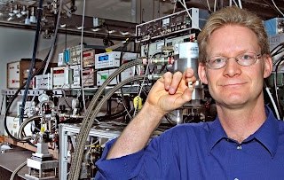
MIKE WANKE, principal investigator of the Terahertz Microelectronics Transceiver Grand Challenge, holds a miniaturized device that will eventually replace large pieces of equipment like those in the background. (Photo by Bill Doty)
Terahertz radiation is of interest because some frequencies can be used to "see through" certain materials. Potentially they could be used in dental or skin cancer imaging to distinguish different tissue types. They also permit improved nondestructive testing of materials during production monitoring. Other frequencies could be used to penetrate clothing, and possibly identify chemical or biological weapons and narcotics.
Since the demonstration of semiconductor THz quantum cascade lasers (QCLs) in 2002, it has been apparent that these devices could offer unprecedented advantages in technologies used for security, communications, radar, chemical spectroscopy, radioastronomy and medical diagnostics.

Until now, however, sensitive coherent transceiver (transmitter/receiver) systems were assembled from a collection of discrete and often very large components. Similar to moving from discrete transistor to integrated chips in the microwave world and moving from optical breadboards to photonic integrated circuits in the visible/infrared world, this work represents the first steps toward reduction in size and enhanced functionality in the THz frequency spectrum.

The work, described in the current issue (June 27, 2010) of "Nature Photonics," represents the first successful monolithic integration of a THz quantum-cascade laser and diode mixer to form a simple, but generically useful, terahertz photonic integrated circuit — a microelectronic terahertz transceiver.

With investment from Sandia's Laboratory-Directed Research and Development (LDRD) program, the lab focused on the integration of THz QCLs with sensitive, high-speed THz Schottky diode detectors, resulting in a compact, reliable solid-state platform. The transceiver embeds a small Schottky diode into the ridge waveguide cavity of a QCL, so that local-oscillator power is directly supplied to the cathode of the diode from the QCL internal fields, with no optical coupling path. ###

The Sandia semiconductor THz development team, headed by Michael Wanke, also included Erik Young, Christopher Nordquist, Michael Cich, Charles Fuller, John Reno, Mark Lee — all of Sandia labs — and Albert Grine of LMATA Government Services, LLC, in Albuquerque. Young recently joined Philips Lumileds Lighting Co., in San Jose, Calif.

Sandia National Laboratories is a multi-program laboratory operated by Sandia Corporation, a wholly owned subsidiary of Lockheed Martin Corporation, for the U.S. Department of Energy's National Nuclear Security Administration. With main facilities in Albuquerque, N.M., and Livermore, Calif., Sandia has major R&D responsibilities in national security, energy and environmental technologies, and economic competitiveness.

Sandia news media contact: Neal Singer, nsinger@sandia.gov (505) 845-7078 Sandia media relations contact: Stephanie Hobby, shobby@sandia.gov (505) 844-0948 WEB: DOE/Sandia National Laboratories

Sunday, July 25, 2010

ESA to set tiny hair-like Webb Telescope microshutters

Tiny little shutters as small as the width of a human hair are a key component in the James Webb Space Telescope's ability to see huge distances in the cosmos, and they have now arrived at the European Space Agency. Those little "shutters" are actually called "microshutters" and they are tiny doorways that focus the attention of the infrared camera on specific targets to the exclusion of others. They will focus in on objects like very distant stars and galaxies.

The microshutters were recently shipped from NASA's Goddard Space Flight Center in Greenbelt, Md. to the European Space Agency (ESA) for installation into the near-infrared spectrograph (NIRSpec) instrument. This is a big step, because the microshutters are components that will fly on the actual telescope.

Harvey Moseley, a Senior Astrophysicist at NASA Goddard, who led the microshutter team, said "This delivery is the culmination of nearly a decade of development, in which the device grew from an initial idea to a revolutionary system for vastly increasing the power of Webb telescope as it probes the distant universe.

Webb Telescope Microshutters

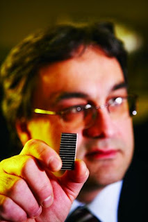
Caption: This is an array of microshutters, about the size of a postage stamp.

Credit: NASA/Chris Gunn. Usage Restrictions: None.

Microshutters Under a Microscope

Caption: This photograph shows microshutters being examined with a microscope. A hair is visible in the picture for size comparison.

Credit: NASA/Chris Gunn. Usage Restrictions: None.
To have completed the development of this device in a space flight program speaks highly of the great team of engineers and technicians who brought this new technology to completion."

The microshutters are assembled as an "array" or collection. An array is a group of tiny microshutters that looks like a little square in a waffle-like grid. Each array or grid contains over 62,000 shutters. Individually, each microshutter measures 100 by 200 microns, or about the width of a human hair. The telescope will contain four of these waffle-looking grids all put together. They also have to work at the incredibly cold temperature of minus 388 degrees Fahrenheit (-233 degrees Celsius).

The microshutters will enable scientists to block unwanted light from objects closer to the camera in space, like light from stars in our Galaxy, letting the light from faraway objects shine through. To get an idea of how these tiny little "hairlike" shutters work, think about how a person raises their hand in front of their eyes to block the sunshine while trying to look at a traffic signal. Microshutters block excess light to see a dim object by blocking out brighter sources of light in the cosmos.

The microshutters were designed, built and tested at NASA's Goddard Space Flight Center in Greenbelt, Md. specifically for the James Webb Space Telescope. They are unique to the Webb telescope.
They will work with the Near Infrared Spectrograph or NIRSpec. That instrument will break up the light from the galaxies into a rainbow of different colors, allowing scientists to determine the kinds of stars and gasses that make up the galaxies and measure their distances and motions. The microshutters help the NIRSpec to separate the light while observing up to 100 objects at the same time, because the microshutter system controls how light enters the NIRSpec.

Engineers at the European Space Agency at EADS/Astrium in Ottobrunn, Germany, a suburb of Munich will install the microshutters into the NIRSpec instrument. Once installed, ESA will conduct further testing on the entire instrument. Once those tests are complete and the NIRSpec is fully-functional and passes all tests, the NIRSpec will return to NASA Goddard to be placed on the main Webb telescope.

The telescope is a joint project of NASA, the European Space Agency and the Canadian Space Agency. ###

Contact: Rob Gutro Robert.J.Gutro@nasa.gov 443-858-1779 NASA/Goddard Space Flight Center

Saturday, July 24, 2010

For platinum catalysts, smaller may be better

When it comes to metal catalysts, the platinum standard is, well, platinum! However, at about $2,000 an ounce, platinum is more expensive than gold. The high cost of the raw material presents major challenges for the future wide scale use of platinum in fuel cells. Research at the U.S. Department of Energy (DOE)'s Lawrence Berkeley National Laboratory (Berkeley Lab) suggests that one possible way to meet these challenges is to think small – really small.

A study led by Gabor Somorjai and Miquel Salmeron of Berkeley Lab's Materials Sciences Division showed that under high pressure, comparable to the pressures at which many industrial technologies operate, nanoparticle clusters of platinum potentially can out-perform the single crystals of platinum now used in fuel cells and catalytic converters.

"We've discovered that the presence of carbon monoxide molecules can reversibly alter the catalytic surfaces of platinum single crystals, supposedly the most thermodynamically stable configuration for a platinum catalyst," said Somorjai, one of the world's foremost experts on surface chemistry and catalysis.

Gabor Somorjai and Miquel Salmeron

Caption: Gabor Somorjai (left), an authority on catalysis, and Miquel Salmeron, an authority on surface imaging, used a high-pressure Scanning Tunneling Microscope to observe the surface of a platinum catalyst under actual industrial reaction conditions.

Credit: Image by Roy Kaltschmidt, Berkeley Lab Public Affairs. Usage Restrictions: None.

Platinum Nanoclusters

Caption: In these STM images of a platinum catalyst, (A) shows the terraced the surface under ultrahigh vacuum, (B) as the surface is covered with carbon monoxide and pressure increases, the terraces widen (C) when coverage is complete and press reaches one torr, the terraces fracture into nanoclusters (D) enlarged view shows triangular shape of the nanoclusters, two of which are marked by red lines.

Credit: (Image courtesy of Berkeley Lab Somorjai and Salmeron, et. al) Usage Restrictions: None.
"This indicates that under high-pressure conditions, single crystals of platinum are not as stable as nanoclusters, which actually become more stabilized as carbon monoxide molecules are co-adsorbed together with platinum atoms."

"Our results also demonstrate that the limitations of traditional surface science techniques can be overcome with the use of techniques that operate under realistic conditions, says Salmeron, a leading authority on surface imaging and developer of the in situ imaging and spectroscopic techniques used in this study. He is also the director of Berkeley Lab's Materials Sciences Division.

In this study, single crystal platinum surfaces were examined under high-pressure. The surfaces were structured as a series of flat terraces about six atoms wide separated by atomic steps. Such structural feature are common in metal catalysts and are considered to be the active sites where catalytic reactions occur. Single crystals are used as models for these features.

Somorjai and Salmeron coated the platinum surfaces in this study with carbon monoxide gas, a reactant involved in many important industrial catalytic processes, including the Fischer-Tropsch process for making liquid hydrocarbons, the oxidation process in automobile catalytic converters, and the degradation of platinum electrodes in hydrogen fuel cells. As carbon monoxide coverage of the platinum crystal surfaces approached 100-percent, the terraces began to widen – the result of increasing lateral repulsion between the molecules. When the surface pressure reached one torr, the terraces fractured into nanometer-sized clusters. The terraces were re-formed upon removal of the carbon monoxide gas.

"Our observations of the large-scale surface restructuring of stepped platinum highlights the strong connection between coverage of reactant molecules and the atomic structure of the catalyst surface," says Somorjai.
"The ability to observe catalytic surfaces at the atomic and molecular levels under actual reaction conditions is the only way such a phenomenon could be detected."

Catalysts – substances that speed up the rates of chemical reactions without themselves being chemically changed – are used to initiate virtually every industrial manufacturing process that involves chemistry. Metal catalysts are the workhorses with platinum being one of the best. Industrial catalysts typically operate under pressures ranging from millitorr to atmospheres, and at temperatures ranging from room to hundreds of degrees Celsius. However, surface science experiments have traditionally been performed under high vacuum conditions and low temperatures.

"Such conditions will likely inhibit any surface restructuring process that requires the overcoming of even moderate activation barriers," Somorjai says.

Says Salmeron, "The unanswered question today is what are the geometry and location of the catalyst atoms when the surfaces are covered with dense layers of molecules, as occurs during a chemical reaction."

Somorjai and Salmeron have for many years been collaborating on the development of instrumentation and techniques that enable them to do catalysis studies under realistic conditions. They now have at their disposal unique high-pressure scanning tunneling microscopes (STM) and an ambient pressure x-ray photoelectron spectroscopy (AP-XPS) beamline operating at the Berkeley Lab's Advanced Light Source, a premier source of synchrotron radiation for scientific research.

"With these two resources, we can image the atomic structure and identify the chemical state of catalyst atoms and adsorbed reactant molecules under industrial-type pressures and temperatures," Salmeron says.

STM images revealed the formation of nanoclusters on the platinum crystal surfaces, and the AP-XPS spectra revealed a change in carbon monoxide electron binding energies. A subsequent collaboration with Lin-Wang Wang, a theorist in Berkeley Lab's Computational Sciences Division, explained the change in structure as the result of the relaxation of the strong repulsion between carbon monoxide molecules that arises from their very high density on the surface when in equilibrium with elevated pressures of the gas.

"In the future, the use of these stable platinum nanoclusters as fuel cell catalysts may help to boost performance and reduce costs," Somorjai says.

The next step for Somorjai and Salmeron and their research team will be to determine whether other adsorbed reactants, such as oxygen or hydrogen, also result in the creation of nanoclusters in platinum. They also want to know if nanoclusters can be induced in other metal catalysts as well, such as palladium, silver, copper, rhodium, iron and cobalt.

"If this nanoclustering is a general phenomenon, it will have major consequences for the type of structures that catalysts must have under high-pressure, high-temperature catalytic reaction conditions," Somorjai says. ###

A paper on this research appears in the journal Science, titled "Break-Up of Stepped Platinum Catalyst Surfaces by High CO Coverage." Co-authoring this paper with Somorjai and Salmeron were Feng Tao, Sefa Dag, Lin-Wang Wang, Zhi Liu, Derek Butcher and Hendrik Bluhm.

This research was supported by the Basic Energy Sciences programs of the DOE Office of Science.

Berkeley Lab is a U.S. Department of Energy national laboratory located in Berkeley, California. It conducts unclassified scientific research for DOE's Office of Science and is managed by the University of California. Visit our Website at www.lbl.gov/

Contact: Lynn Yarris lcyarris@lbl.gov 510-486-5375 DOE/Lawrence Berkeley National Laboratory

Thursday, July 22, 2010

Shape-shifting sheets automatically fold into multiple shapes VIDEO

Relying on origami techniques, researchers show programmable matter folding into a boat- or plane-shape.

Cambridge, Mass., – "More than meets the eye" may soon become more than just a tagline for a line of popular robotic toys.

Researchers at Harvard and MIT have reshaped the landscape of programmable matter by devising self-folding sheets that rely on the ancient art of origami.

Called programmable matter by folding, the team demonstrated how a single thin sheet composed of interconnected triangular sections could transform itself into a boat- or plane-shape—all without the help of skilled fingers.


Caption: A programmable sheet self-folds into a boat- and into a plane-shape.

Credit: Robert Wood, Harvard School of Engineering and Applied Sciences, and Daniella Rus, MIT/CSAIL. Usage Restrictions: None
Published in the online Early Edition of the Proceedings of the National Academy of Sciences (PNAS) during the week of June 28, lead authors Robert Wood, associate professor of electrical engineering at the Harvard School of Engineering and Applied Sciences (SEAS) and a core faculty member of the Wyss Institute for Biologically Inspired Engineering, and Daniela Rus, a professor in the Electrical Engineering and Computer Science department at MIT and co-director of the CSAIL Center for Robotics, envision creating "smart" cups that could adjust based upon the amount of liquid needed or even a "Swiss army knife" that could form into tools ranging from wrenches to tripods.
"The process begins when we first create an algorithm for folding," explains Wood. "Similar to a set of instructions in an origami book, we determine, based upon the desired end shapes, where to crease the sheet."

The sheet, a thin composite of rigid tiles and elastomer joints, is studded with thin foil actuators (motorized switches) and flexible electronics. The demonstration material contains twenty-five total actuators, divided into five groupings. A shape is produced by triggering the proper actuator groups in sequence.

To initiate the on-demand folding, the team devised a series of stickers, thin materials that contain the circuitry able to prompt the actuators to make the folds. This can be done without a user having to access a computer, reducing "programming" to merely placing the stickers in the appropriate places. When the sheet receives the proper jolt of current, it begins to fold, staying in place thanks to magnetic closures.

"Smart sheets are Origami Robots that will make any shape on demand for their user," says Rus. "A big achievement was discovering the theoretical foundations and universality of folding and fold planning, which provide the brain and the decision making system for the smart sheet."

The fancy folding techniques were inspired in part by the work of co-author Erik Dermaine, an associate professor of electrical engineering and computer science at MIT and one of the world's most recognized experts on computational origami.

While the Harvard and MIT engineers only demonstrated two simple shapes, the proof of concept holds promise. The long-term aim is to make programmable matter more robust and practical, leading to materials that can perform multiple tasks, such as an entire dining utensil set derived from one piece of foldable material.

"The Shape-Shifting Sheets demonstrate an end-to-end process that is a first step towards making everyday objects whose mechanical properties can be programmed," concludes Wood. ###

Wood and Rus's co-authors included Elliot Hawkes and Hiroto Tanaka, both at Harvard, and Byoung Kwon An, Nadia Benbernou, Sangbae Kim, and Erik Dermaine, all at MIT.

The authors acknowledge funding from the Defense Advanced Research Projects Agency (DARPA).

Contact: Michael Patrick Rutter mrutter@seas.harvard.edu 617-496-3815 Harvard University

Wednesday, July 21, 2010

Depth Charge: Using Atomic Force Microscopy to Study Subsurface Structures

Over the past couple of decades, atomic force microscopy (AFM) has emerged as a powerful tool for imaging surfaces at astonishing resolutions—fractions of a nanometer in some cases. But suppose you're more concerned with what lies below the surface? Researchers at the National Institute of Standards and Technology (NIST) have shown that under the right circumstances, surface science instruments such as the AFM can deliver valuable data about sub-surface conditions.

Their recently published* work with colleagues from the National Aeronautics and Space Administration (NASA), National Institute of Aerospace, University of Virginia and University of Missouri could be particularly useful in the design and manufacture of nanostructured composite materials. Engineers are studying advanced materials that mix carbon nanotubes in a polymer base for a wide variety of high-performance applications because of the unique properties, such as superior strength and electrical conductance, added by the nanotubes. The material chosen by the research team as their test case, for example, is being studied by NASA for use in spacecraft actuators because it may outperform the heavier ceramics now used.

carbon nanotube composite

Electric force microscopy can be used to detail structures well below the surface. Left, AFM height image showing the surface of a polyimide/carbon nanotube composite. Right, EFM image revealing the curved lines of subsurface nanotubes. Credit: NIST
But, says NIST materials scientist Minhua Zhao, "one of the critical issues to study is how the carbon nanotubes are distributed within the composite without actually breaking the part. There are very few techniques available for this kind of non-destructive study." Zhao and his colleagues decided to try an unusual application of atomic force microscopy.
The AFM is actually a family of instruments working on the same basic principal: a delicate needle-like point hovers just above the surface to be profiled and responds to weak, atomic-level forces. A typical AFM senses so-called "van der Waals forces," very short-range forces exerted by molecules or atoms. This restricts the instrument to the surface of samples.

Instead, the team used an AFM designed to use the stronger, longer-range electrostatic force (technically an EFM), measuring the interaction between the probe tip and a charged plate beneath the composite sample. What makes it work, says Zhao, is that the nanotubes are electrical conductors with high dielectric constant (a measure of how the material affects an electric field), but the polymer is a low dielectric constant material. Such huge dielectric constant differences between nanotubes and the polymer is the key to the success of this technique, and with properly chosen voltages the nanotubes show up as finely detailed fibers dispersed below the composite's surface.

The goal, according to Zhao, is to control the process well enough to allow quantitative measurements. At present the group can discriminate different concentrations of carbon nanotubes in the polymer, determine conductive networks of the nanotubes and map electric potential distribution of the nanotubes below the surface. But the measurement is quite tricky, many factors, including probe shape and even humidity affect the electrostatic force.

The team used a specially designed probe tip and a patented, NIST-designed AFM humidity chamber.** An interesting, not yet fully understood effect, says Zhao, is that increasing the voltage between the probe and the sample at some point causes the image contrast to invert, dark regions becoming light and vice versa. The team is studying the mechanism of such contrast inversion.

"We are still optimizing this EFM technique for subsurface imaging," says Zhao. "If the depth of nanostructures located from the film surface can be determined quantitatively, this technique will be a powerful tool for nondestructive subsurface imaging of high dielectric nanostructures in a low dielectric matrix, with a broad range of applications in nanotechnology." ###

* M.H. Zhao, X.H. Gu, S.E. Lowther, C. Park, Y.C. Jean and T. Nguyen. Subsurface characterization of carbon nanotubes in polymer composites via quantitative electric force microscopy. Nanotechnology 21 (2010) 225702 doi:10.1088/0957-4484/21/22/225702.

** J.W. Martin, E. Embree and M.R. VanLandingham. Humidity Chamber For Stylus Atomic Force With Cantilever. U.S. Patent No. 6,490,913 B1, Dec. 10, 2002.

Contact: Michael Baum michael.baum@nist.gov 301-975-2763 National Institute of Standards and Technology (NIST)

Tuesday, July 20, 2010

Researchers create self-assembling nanodevices that move and change shape on demand

BOSTON, Mass. – By emulating nature's design principles, a team at Harvard's Wyss Institute for Biologically Inspired Engineering, Harvard Medical School and Dana-Farber Cancer Institute has created nanodevices made of DNA that self-assemble and can be programmed to move and change shape on demand. In contrast to existing nanotechnologies, these programmable nanodevices are highly suitable for medical applications because DNA is both biocompatible and biodegradable.

The work appears in the June 20 advance online Nature Nanotechnology.

Built at the scale of one billionth of a meter, each device is made of a circular, single-stranded DNA molecule that, once it has been mixed together with many short pieces of complementary DNA, self-assembles into a predetermined 3D structure. Double helices fold up into larger, rigid linear struts that connect by intervening single-stranded DNA.

A tensegrity built with wooden rods and string

A tensegrity built with wooden rods and string.

diagrammatic image of a tensegrity built with DNA struts

A diagrammatic image of a tensegrity built with DNA struts (shown as colored ladders folded into rods) and DNA cable strands (shown as colored single lines). Light gray arrows show contractile forces exerted by the cable strands, while dark gray arrows show compressive forces along the struts.

electron micrograph of an actual nanoscale tensegrity built using the new DNA-based, self-assembling nanofabrication capabilities

An electron micrograph of an actual nanoscale tensegrity built using the new DNA-based, self-assembling nanofabrication capabilities. Scale bars equal 20 nanometers (billionths of a meter).

Images by Tim Liedl
These single strands of DNA pull the struts up into a 3D form—much like tethers pull tent poles up to form a tent. The structure's strength and stability result from the way it distributes and balances the counteracting forces of tension and compression.

This architectural principle—known as tensegrity—has been the focus of artists and architects for many years, but it also exists throughout nature. In the human body, for example, bones serve as compression struts, with muscles, tendons and ligaments acting as tension bearers that enable us to stand up against gravity. The same principle governs how cells control their shape at the microscale.

"This new self-assembly based nanofabrication technology could lead to nanoscale medical devices and drug delivery systems, such as virus mimics that introduce drugs directly into diseased cells," said co-investigator and Wyss Institute director Don Ingber. A nanodevice that can spring open in response to a chemical or mechanical signal could ensure that drugs not only arrive at the intended target but are also released when and where desired.

Further, nanoscopic tensegrity devices could one day reprogram human stem cells to regenerate injured organs. Stem cells respond differently depending on the forces around them. For instance, a stiff extracellular matrix—the biological glue surrounding cells—fabricated to mimic the consistency of bone signals stem cells to become bone, while a soupy matrix closer to the consistency of brain tissue signals the growth of neurons. Tensegrity nanodevices "might help us to tune and change the stiffness of extracellular matrices in tissue engineering someday," said first author Tim Liedl, who is now a professor at Ludwig-Maximilians-Universität in Munich.

"These little Swiss Army knives can help us make all kinds of things that could be useful for advanced drug delivery and regenerative medicine," said lead investigator William Shih, Wyss core faculty member and associate professor of biological chemistry and molecular pharmacology at HMS and Dana-Farber Cancer Institute. "We also have a handy biological DNA Xerox machine that nature evolved for us," making these devices easy to manufacture.

This new capability "is a welcome element in the structural DNA nanotechnology toolbox," said Ned Seeman, professor of chemistry at New York University. ###

This research was funded by the Wyss Institute for Biologically Inspired Engineering at Harvard University, National Institutes of Health, Deutscher Akademischer Austauschdienst Fellowship, Swedish Science Council Fellowship and Claudia Adams Barr Program Investigator award.

Written by Elizabeth Dougherty

CITATION:

Nature Nanotechnology, online publication, June 20, 2010

“Self-assembly of 3D prestressed tensegrity structures from DNA”

Tim Liedl, Bjorn Hogberg, Jessica Tytell, Donald E. Ingber, William M. Shih

WYSS INSTITUTE CONTACT: Mary Tolikas mary.tolikas@wyss.harvard.edu 617-432-7733

DANA-FARBER CANCER INSTITUTE CONTACT Bill Schaller william_schaller@dfci.harvard.edu 617-632-5357
The Wyss Institute for Biologically Inspired Engineering at Harvard University uses nature’s design principles to create breakthrough technologies that will revolutionize medicine, industry and the environment. Working as an alliance among Harvard’s Medical School, School of Engineering and Applied Sciences, and Faculty of Arts and Sciences, and in partnership with Beth Israel Deaconess Medical Center, Children’s Hospital Boston, Dana-Farber Cancer Institute, University of Massachusetts Medical School and Boston University, the Institute crosses disciplinary and institutional barriers to engage in high-risk, fundamental research that leads to transformative change. By applying biological principles, Wyss researchers are developing innovative new engineering solutions for healthcare, manufacturing, robotics, energy and sustainable architecture. These technologies are translated into commercial products and therapies through collaborations with clinical investigators, corporate alliances and new startups.

Harvard Medical School has more than 7,500 full-time faculty working in 11 academic departments located at the School's Boston campus or in one of 47 hospital-based clinical departments at 17 Harvard-affiliated teaching hospitals and research institutes. Those affiliates include Beth Israel Deaconess Medical Center, Brigham and Women's Hospital, Cambridge Health Alliance, Children's Hospital Boston, Dana-Farber Cancer Institute, Forsyth Institute, Harvard Pilgrim Health Care, Hebrew SeniorLife, Joslin Diabetes Center, Judge Baker Children's Center, Massachusetts Eye and Ear Infirmary, Massachusetts General Hospital, McLean Hospital, Mount Auburn Hospital, Schepens Eye Research Institute, Spaulding Rehabilitation Hospital, and VA Boston Healthcare System.

Contact: David Cameron david_cameron@hms.harvard.edu 617-432-0441 Harvard Medical School

Monday, July 19, 2010

using carbon nanotubes in a lithium battery can dramatically improve its energy capacity.

Batteries might gain a boost in power capacity as a result of a new finding from researchers at MIT. They found that using carbon nanotubes for one of the battery’s electrodes produced a significant increase — up to tenfold — in the amount of power it could deliver from a given weight of material, compared to a conventional lithium-ion battery. Such electrodes might find applications in small portable devices, and with further research might also lead to improved batteries for larger, more power-hungry applications.

To produce the powerful new electrode material, the team used a layer-by-layer fabrication method, in which a base material is alternately dipped in solutions containing carbon nanotubes that have been treated with simple organic compounds that give them either a positive or negative net charge. When these layers are alternated on a surface, they bond tightly together because of the complementary charges, making a stable and durable film.

students Betar Gallant and Seung Woo Lee and professors Yang Shao-Horn and Paula Hammond

From left, students Betar Gallant and Seung Woo Lee and professors Yang Shao-Horn and Paula Hammond, in one of the labs where the use of carbon nanotubes in lithium batteries was researched.
The findings, by a team led by Associate Professor of Mechanical Engineering and Materials Science and Engineering Yang Shao-Horn, in collaboration with Bayer Chair Professor of Chemical Engineering Paula Hammond, are reported in a paper published June 20 in the journal Nature Nanotechnology. The lead authors are chemical engineering student Seung Woo Lee PhD ’10 and postdoctoral researcher Naoaki Yabuuchi.
Batteries, such as the lithium-ion batteries widely used in portable electronics, are made up of three basic components: two electrodes (called the anode, or negative electrode, and the cathode, or positive electrode) separated by an electrolyte, an electrically conductive material through which charged particles, or ions, can move easily. When these batteries are in use, positively charged lithium ions travel across the electrolyte to the cathode, producing an electric current; when they are recharged, an external current causes these ions to move the opposite way, so they become embedded in the spaces in the porous material of the anode.

In the new battery electrode, carbon nanotubes — a form of pure carbon in which sheets of carbon atoms are rolled up into tiny tubes — “self-assemble” into a tightly bound structure that is porous at the nanometer scale (billionths of a meter). In addition, the carbon nanotubes have many oxygen groups on their surfaces, which can store a large number of lithium ions; this enables carbon nanotubes for the first time to serve as the positive electrode in lithium batteries, instead of just the negative electrode.

This “electrostatic self-assembly” process is important, Hammond explains, because ordinarily carbon nanotubes on a surface tend to clump together in bundles, leaving fewer exposed surfaces to undergo reactions. By incorporating organic molecules on the nanotubes, they assemble in a way that “has a high degree of porosity while having a great number of nanotubes present,” she says.

Powerful and stable

Lithium batteries with the new material demonstrate some of the advantages of both capacitors, which can produce very high power outputs in short bursts, and lithium batteries, which can provide lower power steadily for long periods, Lee says. The energy output for a given weight of this new electrode material was shown to be five times greater than for conventional capacitors, and the total power delivery rate was 10 times that of lithium-ion batteries, the team says. This performance can be attributed to good conduction of ions and electrons in the electrode, and efficient lithium storage on the surface of the nanotubes.

In addition to their high power output, the carbon-nanotube electrodes showed very good stability over time. After 1,000 cycles of charging and discharging a test battery, there was no detectable change in the material’s performance.

The electrodes the team produced had thicknesses up to a few microns, and the improvements in energy delivery only were seen at high-power output levels. In future work, the team aims to produce thicker electrodes and extend the improved performance to low-power outputs as well, they say. In its present form, the material might have applications for small, portable electronic devices, says Shao-Horn, but if the reported high-power capability were demonstrated in a much thicker form — with thicknesses of hundreds of microns rather than just a few — it might eventually be suitable for other applications such as hybrid cars.

While the electrode material was produced by alternately dipping a substrate into two different solutions — a relatively time-consuming process — Hammond suggests that the process could be modified by instead spraying the alternate layers onto a moving ribbon of material, a technique now being developed in her lab. This could eventually open the possibility of a continuous manufacturing process that could be scaled up to high volumes for commercial production, and could also be used to produce thicker electrodes with a greater power capacity. “There isn’t a real limit” on the potential thickness, Hammond says. “The only limit is the time it takes to make the layers,” and the spraying technique can be up to 100 times faster than dipping, she says.

Lee says that while carbon nanotubes have been produced in limited quantities so far, a number of companies are currently gearing up for mass production of the material, which could help to make it viable for large-scale battery manufacturing.

Yury Gogotsi, professor of materials science at Drexel University, says, “This is an important achievement, because there is a need for energy storage in a thin-film format for powering portable electronic devices and for flexible, wearable electronics. Bridging the performance gap between batteries and electrochemical capacitors is an important task, and the MIT group has made an important step in this direction.”

Some uncertainties remain, however. “The electrochemical performance data presented in the article may only be valid for relatively thin films with no packaging,” Gogotsi says, pointing out that the measured results were for just the individual electrode, and results might be different for a whole battery with its multiple parts and outer container. “The question remains whether the proposed approach will work for much thicker conventional electrodes, used in devices that are used in hybrid and electric cars, wind power generators, etc.” But, he adds, if it does turn out that this new system works for such thicker electrodes, “the significance of this work will increase dramatically.”

Contact: Jennifer Hirsch jfhirsch@mit.edu 617-253-1682 Massachusetts Institute of Technology

Sunday, July 18, 2010

University of Minnesota researchers clear major hurdle in road to high-efficiency solar cells

A team of University of Minnesota-led researchers has cleared a major hurdle in the drive to build solar cells with potential efficiencies up to twice as high as current levels, which rarely exceed 30 percent.

By showing how energy that is now being lost from semiconductors in solar cells can be captured and transferred to electric circuits, the team has opened a new avenue for solar cell researchers seeking to build cheaper, more efficient solar energy devices. The work is published in this week's Science.

A system built on the research could also slash the cost of manufacturing solar cells by removing the need to process them at very high temperatures.

The achievement crowns six years of work begun at the university Institute of Technology (College of Science and Engineering) chemical engineering and materials science professors Eray Aydil and David Norris and chemistry professor Xiaoyang Zhu (now at the university of Texas-Austin) and spearheaded by U of M graduate student William Tisdale.

Eray Aydil, University of Minnesota

Caption: U of M researchers have cleared a major hurdle in the drive to build solar cells with potential efficiencies up to twice as high as current levels.

Credit: © University of Minnesota. Usage Restrictions: None.
In most solar cells now in use, rays from the sun strike the uppermost layer of the cells, which is made of a crystalline semiconductor substance—usually silicon. The problem is that many electrons in the silicon absorb excess amounts of solar energy and radiate that energy away as heat before it can be harnessed.

An early step in harnessing that energy is to transfer these "hot" electrons out of the semiconductor and into a wire, or electric circuit, before they can cool off. But efforts to extract hot electrons from traditional silicon semiconductors have not succeeded.

However, when semiconductors are constructed in small pieces only a few nanometers wide -- "quantum dots" -- their properties change.

"Theory says that quantum dots should slow the loss of energy as heat," said Tisdale. "And a 2008 paper from the University of Chicago showed this to be true. The big question for us was whether we could also speed up the extraction and transfer of hot electrons enough to grab them before they cooled."
In the current work, Tisdale and his colleagues demonstrated that quantum dots—made not of silicon but of another semiconductor called lead selenide -- could indeed be made to surrender their "hot" electrons before they cooled. The electrons were pulled away by titanium dioxide, another common inexpensive and abundant semiconductor material that behaves like a wire.

"This is a very promising result," said Tisdale. "We've shown that you can pull hot electrons out very quickly – before they lose their energy. This is exciting fundamental science."

The work shows that the potential for building solar cells with efficiencies approaching 66 percent exists, according to Aydil.

"This work is a necessary but not sufficient step for building very high-efficiency solar cells," he said. "It provides a motivation for researchers to work on quantum dots and solar cells based on quantum dots."

The next step is to construct solar cells with quantum dots and study them. But one big problem still remains: "Hot" electrons also lose their energy in titanium dioxide. New solar cell designs will be needed to eliminate this loss, the researchers said.

Still, "I'm comfortable saying that electricity from solar cells is going to be a large fraction of our energy supply in the future," Aydil noted. ###

The research was funded primarily by the U.S. Department of Energy and partially by the National Science Foundation. Other authors of the paper were Brooke Timp from the University of Minnesota and Kenrick Williams from UT-Austin.

Contact: Preston Smith smith@umn.edu 612-625-0552 University of Minnesota

Friday, July 16, 2010

Peering into the never before seen

LIVERMORE, Calif. – Scientists can now peer into the inner workings of catalyst nanoparticles 3,000 times smaller than a human hair within nanoseconds.

The findings point the way toward future work that could greatly improve catalyst efficiency in a variety of processes that are crucial to the world’s energy security, such as petroleum catalysis and catalyst-based nanomaterial growth for next-generation rechargeable batteries. The work was performed in a collaborative effort by Lawrence Livermore National Laboratory and the University of California at Davis.

Using a new imaging technique on Lawrence Livermore’s Dynamic Transmission Electron Microscope (DTEM), researchers have achieved unprecedented spatial and temporal resolution in single-shot images of nanoparticulate catalysts.

dynamic transmission electron microscope

Making adjustments to the dynamic transmission electron microscope. From left: Curtis Brown, Thomas LaGrange and Judy Kim.
The DTEM uses a laser-driven photocathode to produce short pulses of electrons capable of recording electron micrographs with 15-nanosecond (one billionth of a second) exposure time. The recent addition of an annular dark field (ADF) aperture to the instrument has greatly improved its ability to time-resolve images of nanoparticles as small as 30 nanometers in diameter.

“Nanoparticles in this size range are of crucial importance to a wide variety of catalytic process of keen interest to energy and nanotechnology researchers,” said UC Davis’ Dan Masiel, formerly of LLNL and lead author of a paper appearing in the journal, ChemPhysChem.
“Time-resolved imaging of such materials will allow for unprecedented insight into the dynamics of their behavior.”

Previously, particles smaller than 50 nanometers could not be resolved in the 15-nanosecond exposure because of the limited signal and low contrast without ADF aperature. But by using DTEM’s ADF, almost every 50-nanometer particle and many 30-nanometer ones became clearly visible because of the fast time resolution and high contrast.

“The stark difference between these two images clearly demonstrates the efficacy of annual dark field imaging when imaging samples with feature sizes near the resolution limit of DTEM,” Masiel said.

The new technique makes it easier to discern significant features when compared to bright field pulsed imaging. It allows for vastly improved contrast for smaller particles, widening the range of catalyst systems that can be studied using DTEM.

DTEM can record images with six orders of magnitude higher temporal resolution than conventional TEM and can provide important insights into processes such as phase transformations, chemical reactions and nanowire and nanotube growth.

Co-authors include LLNL’s Bryan Reed, Thomas LaGrange, Geoffrey Campbell, Ting Guo and Nigel Browning. The work was funded by the Department of Energy’s Office of Science, Office of Basic Energy Sciences, Materials Sciences and Engineering Division.

The article appears in the online edition of ChemPhys Chem.

Founded in 1952, Lawrence Livermore National Laboratory is a national security laboratory, with a mission to ensure national security and apply science and technology to the important issues of our time. Lawrence Livermore National Laboratory is managed by Lawrence Livermore National Security, LLC for the U.S. Department of Energy's National Nuclear Security Administration.

Contact: Anne Stark stark8@llnl.gov 925-422-9799 DOE/Lawrence Livermore National Laboratory
Thursday, July 15, 2010

Researchers develop ultra-simple method for creating nanoscale gold coatings VIDEO

Rensselaer Polytechnic Institute study details new process for creating monolayers of gold nanoparticles; holds promise for new nanoelectronics applications.

Troy, N.Y. – Researchers at Rensselaer Polytechnic Institute have developed a new, ultra-simple method for making layers of gold that measure only billionths of a meter thick. The process, which requires no sophisticated equipment and works on nearly any surface including silicon wafers, could have important implications for nanoelectronics and semiconductor manufacturing.

Sang-Kee Eah, assistant professor in the Department of Physics, Applied Physics, and Astronomy at Rensselaer, and graduate student Matthew N. Martin infused liquid toluene – a common industrial solvent – with gold nanoparticles. The nanoparticles form a flat, closely packed layer of gold on the surface of the liquid where it meets air. By putting a droplet of this gold-infused liquid on a surface, and waiting for the toluene to evaporate, the researchers were able to successfully coat many different surfaces – including a 3-inch silicon wafer – with a monolayer of gold nanoparticles.


"There has been tremendous progress in recent years in the chemical syntheses of colloidal nanoparticles. However, fabricating a monolayer film of nanoparticles that is spatially uniform at all length scales – from nanometers to millimeters – still proves to be quite a challenge," Eah said. "We hope our new ultra-simple method for creating monolayers will inspire the imagination of other scientists and engineers for ever-widening applications of gold nanoparticles."

Whereas other synthesis methods take several hours, this new method chemically synthesizes gold nanoparticles in only 10 minutes without the need for any post-synthesis cleaning, Eah said. In addition, gold nanoparticles created this way have the special property of being charged on non-polar solvents for 2-D self-assembly.

Previously, the 2-D self-assembly of gold nanoparticles in a toluene droplet was reported with excess ligands, which slows down and complicates the self-assembly process. This required the non-volatile excess ligands to be removed in a vacuum. In contrast, Eah's new method ensures that gold nanoparticles float to the surface of the toluene drop in less than one second, without the need for a vacuum. It then takes only a few minutes for the toluene droplet to evaporate and leave behind the gold monoloayer.

"The extension of this droplet 2-D self-assembly method to other kinds of nanoparticles, such as magnetic and semiconducting particles, is challenging but holds much potential," Eah said. "Monolayer films of magnetic nanoparticles, for instance, are important for magnetic data storage applications. Our new method may be able to help inform new and exciting applications." ###

Co-authors on the paper are former Rensselaer undergraduate researchers James I. Basham '07, who is now a graduate student at Pennsylvania State University, and Paul Chando '09, who will begin graduate study in the fall at the City College of New York.

The research project was supported by Rensselaer, the Rensselaer Summer Undergraduate Research Program, the National Science Foundation (NSF) Research Experiences for Undergraduates, and the NSF's East Asia and Pacific Summer Institutes and Japan Society for the Promotion of Science.

For more information, visit Eah's website at: www.rpi.edu/~eahs.

Contact: Michael Mullaney Rensselaer Polytechnic Institute Troy, NY 518-276-6161 (office) 518-698-6336 (mobile) mullam@rpi.edu

Wednesday, July 14, 2010

World of lights in the microcosmos

Television screens are becoming increasingly flatter - some have even become almost as thin as a sheet of paper. Their size takes impressive dimensions, much to the delight of home cinema fans. Cellphones and laptops also have ever brighter and more brilliant displays. All of these developments owe their thanks to miniature light-emitting diodes – LEDs – that beam background lighting into a multitude of devices.

World of Lights in the Microcosmos

Caption: The superficial structures of this sheet are only a few micrometers in size.

Credit: Fraunhofer IPT. Usage Restrictions: The picture may be used for editorial purposes only. It is protected by copyright. The use is free of charge if the reference is mentioned.
However, LED technology does have a disadvantage. It is a point light source. But displays are two-dimensional. So how does one distribute the light from an LED evenly on as large a surface as possible, without massive energy loss? At the Fraunhofer Institute for Production Technology IPT in Aachen, a truly one-of-a-kind machine is currently emerging. They will soon be producing fiber optic film that solves this problem and distributes the light two-dimensionally. What's so unusual and special about this: The films possess superficial structures measuring in the single-digit micrometer range, while the sheets themselves measure at two by one meter in size.
This makes them the largest of their kind throughout the EU. In addition, they can be produced cost-effectively and with energy-efficiency in mass reproduction.

To do so, the researchers of IPT developed a process chain with which they can populate large-scale sheets with the necessary microstructures. »It's an ultraprecise process,« says Dr. Christian Wenzel, senior engineer at IPT. Using pinpoint accuracy, the machine must apply the smallest structures – just a few micrometers in size – onto the surface of the film in a periodic sequence. »In order to produce the stamp, we use special diamond tools,« explains Wenzel. The stamp consists of a gossamer-thin nickel sheet, and itself is also infinitesimal: Its surface equals at most two by two millimeters. Like a dot matrix printer, it must then process a sheet measuring two by one meter in size, guided by the ultraprecision machine. »Within a few days, we completely structured the entire surface. With the previous approach, the process would have taken weeks, or even months,« says Wenzel. The preliminary product is the master: a transparent and optically conductive plastic panel.

In order to determine if the microstructured master possesses the desired characteristics, it must first be tested based on a few parameters. »The machine can accomplish this task as well,« says Wenzel. If the approximately 80 percent of the surface is completely structured, the machine tests the properties of the sheet. If these properties are not consistent with the optical design settings, then the machine can implement the necessary corrections during the imprint process. »Well, we are optimizing the component while it's still in the machine,« as Wenzel explains the advantages. Once the plastic surface has the desired light control capabilities, then the engineers immerse the master into a nickel bath and galvanize it. The nickel shim created in this manner can then go into mass replication.

»With our ultraprecise machine, we are capable of producing an entire array of systems with background lighting,« says Wenzel. No matter if it's for displays, architectural lighting or a car's interior lighting: IPT researchers can implement almost any optical design, thanks to this machine, and adapt the machine technology – reliably, and above all, efficiently. In other words: ready for mass production. ###

Contact: Dr.-Ing. Christian Wenzel christian.wenzel@ipt.fraunhofer.de 49-241-890-4220 Fraunhofer-Gesellschaft

Tuesday, July 13, 2010

Texas Tech, U of Utah win Sandia microdevice competition

World's smallest chess set and a microbarbershop win big.

ALBUQUERQUE, N.M. – The world's smallest chess board — about the diameter of four human hairs — and a pea-sized microbarbershop were winners in this year's design contest for, respectively, novel and educational microelectromechanical systems (MEMS), held at Sandia National Laboratories in mid May.

The two winning teams will see their designs birthed in Sandia's microfabrication facility, one of the most advanced in the world.

The micro chess board, created by students at Texas Tech, comes with micropieces scored with the design of traditional chess figures. Each piece is outfitted with even tinier stubs that allow a microrobotic arm to move them from square to square. Space along the side of the board is available to hold captured pieces.

microbarbershop

Caption: The University of Utah's microbarbershop has all the components necessary to cut hair -- a single hair, that is.

Credit: Sandia National Laboratories. Usage Restrictions: Educational and news use.

nano Chessboard

Caption: A playable chessboard -- (just left of center in the image above) is one of the numerous components on the Texas Tech winning entry in this year's MEMS challenge.

Credit: Sandia National Laboratories. Usage Restrictions: Educational and news use.
The microbarbershop, intended to service a single hair, employs a microgripper, cutter, moveable mirror and blow dryer designed by students at the University of Utah. "Our device is so small that a single misty drop of an Irish drizzle would swamp the scissors and drown the device," says team advisor Ian Harvey, a professor of mechanical engineering at the university.

The high-spirited contest, open to institutional members of the Sandia-led MEMS University Alliance program, provides an arena for the nation's student engineers to hone their skills in designing and using microdevices. Such devices are used to probe biological cells, arrange and operate components of telecommunications and high-tech machinery and operate many home devices.

The contest helps develop a sense of the maximum and minimum displacement of a micro object, the amount of force needed to move it and the degrees of freedom needed for a part to accomplish its preset task.

The two winning teams will see their designs birthed in Sandia's microfabrication facility, one of the most advanced in the world.
The micro chess board, created by students at Texas Tech, comes with micropieces scored with the design of traditional chess figures. Each piece is outfitted with even tinier stubs that allow a microrobotic arm to move them from square to square. Space along the side of the board is available to hold captured pieces.

The microbarbershop, intended to service a single hair, employs a microgripper, cutter, moveable mirror and blow dryer designed by students at the University of Utah. "Our device is so small that a single misty drop of an Irish drizzle would swamp the scissors and drown the device," says team advisor Ian Harvey, a professor of mechanical engineering at the university.

The high-spirited contest, open to institutional members of the Sandia-led MEMS University Alliance program, provides an arena for the nation's student engineers to hone their skills in designing and using microdevices. Such devices are used to probe biological cells, arrange and operate components of telecommunications and high-tech machinery and operate many home devices.

The contest helps develop a sense of the maximum and minimum displacement of a micro object, the amount of force needed to move it and the degrees of freedom needed for a part to accomplish its preset task.

Texas Tech's chess board is 435 micrometers by 435 micrometers. (A human hair is about 100 micrometers in diameter.) Each chess piece is approximately 50 micrometers, or half the width of a human hair. The design integrates bidirectional linear drives that enable the movement of pieces longitudinally, a positioning stage with two degrees of freedom and, apparently, the world's smallest chess board.

The University of Utah's microbarbershop consists of a microgripper that reaches off the chip to grasp a human hair and holds it in front of an off-chip deployed microbuzzsaw to be cut. Both microtools, driven by a ratcheting actuator, will be observed at a video-enabled station and portrayed on a large video monitor as they move and cut a human hair. Also included are a moveable micromirror, an off-chip micro hair dryer and an off-chip single-hair "teaser" to complete the playful notion of a barbershop and convey an intuitive sense of relative scale for these tiny machines.

Contributing to Texas Tech's success were Sahil Oak, Sandesh Rawool, Ganapathy Sivakumar and Ashwin Vijayasai, says team advisor and electrical engineering professor Tim Dallas.

Leading the Utah effort were Austin Welborn, Brian Baker, Kurtis Ford, Alex Hogan, Ted Kempe, Keng-Min Lin, Charles Fisher and advisor Ian Harvey.

This year's contest participants included the Air Force Institute of Technology, the universities of Oklahoma and New Mexico and the Central New Mexico Community College.

The MEMS University Alliance is part of Sandia's outreach to universities to improve engineering education. It is open to any US institution of higher learning. The alliance provides classroom teaching materials and licenses for Sandia's special SUMMiT V™ design tools at a reasonable cost. This makes it possible for a university without its own fabrication facilities to develop a curriculum in MEMS. The design competition is an increasing activity within the University Alliance, which now has more than 20 members.

The entire process takes almost nine months. It starts with students developing ideas for a device, followed by creation of an accurate computer model of a design that might work, analysis of the design and, finally, design submission. Sandia's MEMS experts and university professors review the design and determine the winners.

Sandia's state-of-the-art MESA fabrication facility then creates parts for each of the entrants. The SUMMiT V™ fabrication process makes MEMS devices with five levels of polysilicon, the most of any standard process, and is especially well-suited for making complex mechanisms such as gear drive trains. The design competition capitalizes on Sandia's confidence in achieving first-pass fabrication success, which restricts the entire process to a reasonable student timeframe.

Fabricated parts are shipped back to the university students for lengthy tests to determine whether the final product matches the purpose of the original computer simulation.

The University Alliance coordinates with the Sandia-led National Institute for Nano Engineering (NINE), providing additional opportunities for students to self-direct their engineering education, and the Sandia/Los Alamos Center for Integrated Nanotechnologies (CINT), a DOE Office of Science center with the most up-to-date nanotechnology tools. ###

For more information regarding the University Alliance and the design competition, contact Stephanie Johnson at srjohns@sandia.gov .

Sandia National Laboratories is a multi-program laboratory operated by Sandia Corporation, a wholly owned subsidiary of Lockheed Martin Corporation, for the U.S. Department of Energy's National Nuclear Security Administration. With main facilities in Albuquerque, N.M., and Livermore, Calif., Sandia has major R&D responsibilities in national security, energy and environmental technologies, and economic competitiveness.

Sandia news media contact: Neal Singer, nsinger@sandia.gov (505) 845-7078

Contact: Neal Singer nsinger@sandia.gov 505-845-7078 DOE/Sandia National Laboratories