Wednesday, June 30, 2010

Nanosponge drug delivery system more effective than direct injection

When loaded with an anticancer drug, a delivery system based on a novel material called nanosponge is three to five times more effective at reducing tumor growth than direct injection.

That is the conclusion of a paper published in the June 1 issue of the journal Cancer Research.

"Effective targeted drug delivery systems have been a dream for a long time now but it has been largely frustrated by the complex chemistry that is involved," says Eva Harth, assistant professor of chemistry at Vanderbilt, who developed the nanosponge delivery system. "We have taken a significant step toward overcoming these obstacles."

The study was a collaboration between Harth's laboratory and that of Dennis E. Hallahan, a former professor of radiation oncology at Vanderbilt who is now at the Washington University School of Medicine.

Nanosponge Particle Illustration

Caption: The illustration shows a nanosponge particle attaching to human breast cancer cells. The particle holds an anticancer drug that it releases gradually as it decomposes. Peptide linkers are shown with the ball and stick representation. Although only two are shown in the illustration, about three dozen are attached to the surface of actual particles. The linkers are specially configured to bind to the surface of irradiated cancer cells.

Credit: Harth Laboratory. Usage Restrictions: None.
Corresponding authors are Harth and Roberto Diaz at Emory University, who was working in the Hallahan laboratory when the studies were done.

To visualize Harth's delivery system, imagine making tiny sponges that are about the size of a virus, filling them with a drug and attaching special chemical "linkers" that bond preferentially to a feature found only on the surface of tumor cells and then injecting them into the body. The tiny sponges circulate around the body until they encounter the surface of a tumor cell where they stick on the surface (or are sucked into the cell) and begin releasing their potent cargo in a controllable and predictable fashion.
Targeted delivery systems of this type have several basic advantages: Because the drug is released at the tumor instead of circulating widely through the body, it should be more effective for a given dosage. It should also have fewer harmful side effects because smaller amounts of the drug come into contact with healthy tissue.

"We call the material nanosponge, but it is really more like a three-dimensional network or scaffold," says Harth. The backbone is a long length of polyester. It is mixed in solution with small molecules called cross-linkers that act like tiny grappling hooks to fasten different parts of the polymer together. The net effect is to form spherically shaped particles filled with cavities where drug molecules can be stored. The polyester is biodegradable, so it breaks down gradually in the body. As it does, it releases the drug it is carrying in a predictable fashion.

"Predictable release is one of the major advantages of this system compared to other nanoparticle delivery systems under development," says Harth. When they reach their target, many other systems unload most of their drug in a rapid and uncontrollable fashion. This is called the burst effect and makes it difficult to determine effective dosage levels.

Another major advantage is that the nanosponge particles are soluble in water. Encapsulating the anti-cancer drug in the nanosponge allows the use of hydrophobic drugs that do not dissolve readily in water. Currently, these drugs must be mixed with another chemical, called an adjuvant reagent, that reduces the efficacy of the drug and can have adverse side-effects.

It is also possible to control the size of nanosponge particles. By varying the proportion of cross-linker to polymer, the nanosponge particles can be made larger or smaller. This is important because research has shown that drug delivery systems work best when they are smaller than 100 nanometers, about the depth of the pits on the surface of a compact disc. The nanosponge particles used in the current study were 50 nanometers in size. "The relationship between particle size and the effectiveness of these drug delivery systems is the subject of active investigation," says Harth.

The other major advantage of Harth's system is the simple chemistry required. The researchers have developed simple, high-yield "click chemistry" methods for making the nanosponge particles and for attaching the linkers, which are made from peptides, relatively small biological molecules built by linking amino acids. "Many other drug delivery systems require complicated chemistry that will be difficult to scale up for commercial production, but we have continually kept this in mind," Harth says.

The targeting peptide used in the animal studies was developed by the Hallahan laboratory, which also tested the system's effectiveness in tumor-bearing mice. The peptide used in the study is one that selectively binds to tumors that have been treated with radiation.

The drug used for the animal studies was paclitaxel (the generic name of the drug Taxol) that is used in cancer chemotherapy. The researchers recorded the response of two different tumor types – slow-growing human breast cancer and fast-acting mouse glioma – to single injections. In both cases they found that it increased the death of cancer cells and delayed tumor growth "in a manner superior to know chemotherapy approaches."

The next step is to perform an experiment with repeated injections to see if the nanosponge system can stop and reverse tumor growth. Harth is also planning to perform the more comprehensive toxicity studies on her nanoparticle delivery system that are required before it can be used in clinical trials. ###

Additional participants in the study were Ralph J. Passarella, Daniel E. Spratt, John G. Phillips, Hongmei Wu and Li Zhou from the Vanderbilt University Medical Center and Alice E. van der Ende and Vasanth Sathiyakumar from Vanderbilt's Department of Chemistry.

The research was supported by grants from the Department of Defense, National Science Foundation and National Institutes of Health.

Contact: David F. Salisbury david.salisbury@vanderbilt.edu 615-343-6803 Vanderbilt University

Tuesday, June 29, 2010

Copper nanowires enable bendable displays and solar cells

DURHAM, N.C. – A team of Duke University chemists has perfected a simple way to make tiny copper nanowires in quantity. The cheap conductors are small enough to be transparent, making them ideal for thin-film solar cells, flat-screen TVs and computers, and flexible displays.

"Imagine a foldable iPad," said Benjamin Wiley, an assistant professor of chemistry at Duke. His team reports its findings online this week in Advanced Materials.

Nanowires made of copper perform better than carbon nanotubes, and are much cheaper than silver nanowires, Wiley said.

The latest flat-panel TVs and computer screens produce images by an array of electronic pixels connected by a transparent conductive layer made from indium tin oxide (ITO). ITO is also used as a transparent electrode in thin-film solar cells.

copper nanowires

Tiny copper wires can be built in bulk and then "printed" on a surface to conduct current, transparently. | Benjamin Wiley, Duke Chemistry
But ITO has drawbacks: it is brittle, making it unsuitable for flexible screens; its production process is inefficient; and it is expensive and becoming more so because of increasing demand.

"If we are going to have these ubiquitous electronics and solar cells," Wiley said, "we need to use materials that are abundant in the earth's crust and don't take much energy to extract." He points out that there are very few materials that are known to be both transparent and conductive, which is why ITO is still being used despite its drawbacks.
However, Wiley's new work shows that copper, which is a thousand times more abundant than indium, can be used to make a film of nanowires that is both transparent and conductive.

Silver nanowires also perform well as a transparent conductor, and Wiley contributed to a patent on the production of them as a graduate student. But silver, like indium, is rare and expensive. Other researchers have been trying to improve the performance of carbon nanotubes as a transparent conductor, but without much luck.

"The fact that copper nanowires are cheaper and work better makes them a very promising material to solve this problem," Wiley said.

Wiley and his students, PhD candidate Aaron Rathmell and undergraduate Stephen Bergin, grew the copper nanowires in a water-based solution. "By adding different chemicals to the solution, you can control the assembly of atoms into different nanostructures," Wiley said. In this case, when the copper crystallizes, it first forms tiny "seeds," and then a single nanowire sprouts from each seed. It's a mechanism of crystal growth that has never been observed before.

Because the process is water-based, and because copper nanowires are flexible, Wiley thinks the nanowires could be coated from solution in a roll-to-roll process, like newspaper printing, which would be much more efficient than the ITO production process.

Other researchers have produced copper nanowires before, but on a much smaller scale.

Wiley's lab is also the first to demonstrate that copper nanowires perform well as a transparent conductor. He said the process will need to be scaled up for commercial use, and he's got a couple of other problems to solve as well: preventing the nanowires from clumping, which reduces transparency, and preventing the copper from oxidizing, which decreases conductivity. Once the clumping problem has been worked out, Wiley believes the conductivity of the copper nanowires will match that of silver nanowires and ITO.

Wiley, who has applied for a patent for his process, expects to see copper nanowires in commercial use in the not-too-distant future. He notes that there is already investment financing available for the development of transparent conductors based on silver nanowires.

"We think that using a material that is a hundred times cheaper will be even more attractive to venture capitalists, electronic companies and solar companies who all need these transparent electrodes," he said. ###

Contact: Karl Leif Bates karl.bates@duke.edu 919-681-8054 Duke University

Monday, June 28, 2010

Faster computers with nanotechnology

The silicon transistors in your computer may be replaced in ten years by transistors based on carbon nanotubes. This is what scientists at the University of Gothenburg are hoping – they have developed a method to control the nanotubes during production.

Silicon is subject to certain limitations, and industry is looking for a replacement. The electronics industry has net annual sales of over USD 200 billion, and this means that the development is being fuelled by powerful forces.

Carbon nanotubes

Scientist Johannes Svensson from the Department of Physics at the University of Gothenburg has investigated the manufacture and use of carbon nanotubes in his PhD thesis.

Johannes Svensson, University of Gothenburg

Caption: Johannes Svensson is the author of the thesis, "Carbon Nanotube Transistors: Nanotube Growth, Contact Properties and Novel Devices."

Credit: Niklas Olofsson. Usage Restrictions: None.
Faster and smaller

"I don't believe that it will be cheaper to build transistors from another material than silicon, but carbon nanotubes can be used to produce smaller and faster components. This will also result in computers that consume less energy" says Johannes Svensson.

Amazing development

The amazing development in computer power that has taken place after the invention of the integrated circuit in the 1950s has been made possible by the transistor,
which is the most important component of all processors, becoming ever-faster.

Increase the speed

The most common semiconductor material in transistors is silicon, since it is cheap and easy to process. But silicon has its limitations. As the size of the transistors is reduced in order to increase their speed, problems arise that lead to, among other things, increased energy consumption and large variation in the transistor properties.

Pure carbon

By exchanging the silicon in the channel for a carbon nanotube, the transistors can be made both smaller and faster than today's transistors. A carbon nanotube is a molecule in form of a hollow cylinder with a diameter of around a nanometer (roughly 1/50,000 of the width of a human hair) which consists of pure carbon. Some carbon nanotubes are semiconducting, and this means that they can be used in transistors, although there are several problems that must be solved before they can be connected together to form large circuits.

Electric guidance

"Carbon nanotubes grow randomly and it is not possible to control either their position or direction. Therefore I have applied an electrical field to guide the tubes as they grow", says Johannes Svensson.

Built his own

One of the effects of the electric field is that most of the carbon nanotubes lie in the same direction.

"In order to show that it is possible to build electronic components that contain only carbon nanotubes, I have built a transistor which not only has a carbon nanotube as its channel, but also another nanotube which is used as the electrode that controls the current."

Good contacts

Another problem that must be solved when integrating nanotubes into larger circuits is the difficulty of manufacturing good metal contacts for the tubes. Johannes' research has shown that the properties of the contacts depend on the diameter of the nanotubes. Choosing the correct diameter will allow good contacts with a low resistance to be achieved. ###

The thesis Carbon Nanotube Transistors: Nanotube Growth, Contact Properties and Novel Devices was successfully defended at a disputation held on 7 May 2010.

Contact: Johannes Svensson johannes@physics.gu.se 46-317-723-435 University of Gothenburg

Saturday, June 26, 2010

Robots big and small showcase their skills at NIST Alaskan events VIDEO

Make room, Bender, Rosie and R2D2! Your newest mechanical colleagues are a few steps closer to reality, thanks to lessons learned during two robotics events hosted by the National Institute of Standards and Technology (NIST) at the recent IEEE International Conference on Robotics and Automation (ICRA) in Anchorage, Alaska. The events—the Virtual Manufacturing Automation Competition (VMAC) and the Mobile Microrobotics Challenge (MMC)—were designed to prove the viability of advanced technologies for robotic automation of manufacturing and microrobotics.

In the first of two VMAC matches, contestants used off-the-shelf computer gaming engines to run simulations of a robot picking up boxes of various sizes and weights from a conveyor belt and arranging them on a pallet for shipping. The two teams in the competition—both from Georgia Tech University—showed that their systems were capable of solving mixed palletizing challenges.


Caption: In a series of video clips, competition robots and pallet-stacking simulations show their moves.

Credit: NIST. Usage Restrictions: None.
To do this, the system had to receive a previously unseen order list, create a logical plan for stacking and arranging boxes on a pallet to fulfill that order, and then computer simulate the process to show that the plan worked. Getting all of the boxes onto the pallet is relatively straightforward; however, creating a stable, dense pallet is a difficult challenge for a robot.

The second manufacturing contest "road tested" a robot's mobility in a one-third scale factory environment.
The lone participating team, the University of Zagreb (Croatia), demonstrated that it could successfully deliver packages simultaneously to different locations in the mock factory by controlling three robotic Automated Guided Vehicles (AGVs) at once.

In the microrobotics match-up, six teams from Canada, Europe and the United States pitted their miniature mechanisms—whose dimensions are measured in micrometers (millionths of a meter)—against each other in three tests: a two-millimeter dash in which microbots sprinted across a distance equal to the diameter of a pin head; a microassembly task inserting pegs into designated holes; and a freestyle competition showcasing a robot's ability to perform a specialized activity emphasizing one or more of the following: system reliability, level of autonomy, power management and task complexity.

In the two-millimeter dash, the microbot from Carnegie Mellon University broke the world record held by Switzerland's ETH Zurich (the event also was part of earlier NIST-hosted "nanosoccer" competitions) with an average time of 78 milliseconds. However, the achievement was short-lived. Less than an hour later, the French team (representing two French research agencies: the FEMTO-ST Institute and the Institut des Systèmes Intelligents et de Robotique, or ISIR) shattered the mark with an average time of 32 milliseconds.

ETH Zurich was the champion in the microassembly event with a perfect 12 for 12 score steering pegs approximately 500 micrometers long (about the size of a dust particle) into holes at the edge of a microchip. Runner-up was Carnegie Mellon whose microbot successfully placed 4 of 9 pegs.

ETH Zurich's robot also captured the freestyle event, amazing spectators with its unprecedented ability to maneuver in three dimensions within a water medium. In fact, in one demonstration, the Swiss device "flew" over the edge of the microassembly field, reversed direction and pushed out the pegs it had inserted earlier. Taking second place in the freestyle event was the team from Carnegie Mellon that demonstrated how three microbots could be combined into a single system and then disassembled again into separate units. Third place in the event went to the microbot from the Stevens Institute of Technology.

NIST conducted the VMAC in cooperation with IEEE and Georgia Tech, and collaborated on the MMC with the IEEE Robotics and Automation Society. More events of this kind with evolving challenges are planned for the future, as robotics technologies mature. NIST will work with university and industry partners on these events with the goal of advancing skills that future robots—both full-size and micro-size—will need to carry out their functions. ###

Contact: Michael E. Newman michael.newman@nist.gov 301-975-3025 National Institute of Standards and Technology (NIST)

Thursday, June 24, 2010

Applied physicists create building blocks for a new class of optical circuits

Scalable devices inspired by nature exhibit customizable optical properties suitable for applications ranging from highly sensitive sensors and detectors to invisibility cloaks.

CAMBRIDGE, Mass., – Imagine creating novel devices with amazing and exotic optical properties not found in Nature—by simply evaporating a droplet of particles on a surface.

By chemically building clusters of nanospheres from a liquid, a team of Harvard researchers, in collaboration with scientists at Rice University, the University of Texas at Austin, and the University of Houston, has developed just that.

The finding, published in the May 28 issue of Science, demonstrates simple scalable devices that exhibit customizable optical properties suitable for applications ranging from highly sensitive sensors and detectors to invisibility cloaks.

Schematics of Two Optical Circuits

Caption: Schematics of two types of optical circuits: the three particle trimer functions as a nanoscale magnet, while the seven particle heptamer exhibits almost no scattering for a narrow range of wavelengths due to interference.

Credit: The laboratory of Federico Cappaso, Harvard School of Engineering and Applied Sciences. Usage Restrictions: None.
Using particles consisting of concentric metallic and insulating shells, Jonathan Fan, a graduate student at the Harvard School of Engineering and Applied Sciences (SEAS), his lead co-author Federico Capasso, Robert L. Wallace Professor of Applied Physics and Vinton Hayes Senior Research Fellow in Electrical Engineering at SEAS, and Vinothan Manoharan, Associate professor of Chemical Engineering and Physics at SEAS and Harvard's Physics Department, devised a bottom-up, self-assembly approach to meet the design challenge.

"A longstanding challenge in optical engineering has been to find ways to make structures of size much smaller than the wavelength that exhibit desired and interesting properties," says Fan. "At visible frequencies, these structures must be nanoscale."

In contrast, most nanoscale devices are fabricated using top-down approaches, akin to how computer chips are manufactured. The smallest sizes that can be realized by such techniques are severely constrained by the intrinsic limits of the fabrication process, such as the wavelength of light used in the process.
Moreover, such methods are restricted to planar geometries, are expensive, and require intense infrastructure such as cleanrooms.

"With our bottom-up approach, we mimic the way nature creates innovative structures, which exhibit extremely useful properties," explains Capasso. "Our nanoclusters behave as tiny optical circuits and could be the basis of new technology such as detectors of single molecules, efficient and biologically compatible probes in cancer therapeutics, and optical tweezers to manipulate and sort out nano-sized particles. Moreover, the fabrication process is much simpler and cheaper to carry out."

The researcher's self-assembly method requires nothing more than a bit of mixing and drying. To form the clusters, the particles are first coated with a polymer, and a droplet of them is then evaporated on a water-repellent surface. In the process of evaporation, the particles pack together into small clusters. Using polymer spacers to separate the nanoparticles, the researchers were able to controllably achieve a two nanometer gap between the particles—far better resolution than traditional top-down methods allow.

Two types of resulting optical circuits are of considerable interest. A trimer, comprising three equally-spaced particles, can support a magnetic response, an essential property of invisibility cloaks and materials that exhibit negative refractive index.

"In essence, the trimer acts as a nanoscale resonator that can support a circulating loop of current at visible and near-infrared frequencies," says Fan. "This structure functions as a nanoscale magnet at optical frequencies, something that natural materials cannot do."

Heptamers, or packed seven particle structures, exhibit almost no scattering for a narrow range of well-defined colors or wavelengths when illuminated with white light. These sharp dips, known as Fano resonances, arise from the interference of two modes of electron oscillations, a "bright" mode and a non-optically active "dark" mode, in the nanoparticle.

"Heptamers are very efficient at creating extremely intense electric fields localized in nanometer-size regions where molecules and nanoscale particles can be trapped, manipulated, and detected. Molecular sensing would rely on detecting shifts in the narrow spectra dips," says Capasso.

Ultimately, all of the self-assembled circuit designs can be readily tuned by varying the geometry, how the particles are separated, and the chemical environment. In short, the new method allows a "tool kit" for manipulating "artificial molecules" in such a way to create optical properties at will, a feature the researchers expect is broadly generalizable to a host of other characteristics.

Looking ahead, the researchers plan to work on achieving higher cluster yields and hope to assemble three-dimensional structures at the macroscale, a "holy grail" of materials science.

"We are excited by the potentially scalability of the method," says Manoharan. "Spheres are the easiest shapes to assemble as they can be readily packed together. While we only demonstrated here planar particle clusters, our method can be extended to three-dimensional structures, something that a top-down approach would have difficulty doing." ###

Fan, Capasso, and Manoharan's co-authors included Chihhui Wu and Gennady Shvets of University of Texas at Austin; Jiming Bao of the University of Houston; and Kui Bao, Rizia Bardhan, Naomi Halas, and Peter Norlander, all of Rice University.

The researchers acknowledge the support of National Science Foundation, the Air Force Office of Scientific Research; the U.S. Department of Defense; the Robert A. Welch Foundation; and the Center for Advanced Solar Photophysics, a U.S. Department of Energy Frontier Research Center. The work was carried out at the Center for Nanoscale Systems at Harvard, a member of the National Nanotechnology Infrastructure Network.

Contact: Michael Patrick Rutter mrutter@seas.harvard.edu 617-496-3815 Harvard University

Wednesday, June 23, 2010

Optical Legos: Building nanoshell structures

Self-assembly method yields materials with unique optical properties.

HOUSTON -- Scientists from four U.S. universities have created a way to use Rice University's light-activated nanoshells as building blocks for 2-D and 3-D structures that could find use in chemical sensors, nanolasers and bizarre light-absorbing metamaterials. Much as a child might use Lego blocks to build 3-D models of complex buildings or vehicles, the scientists are using the new chemical self-assembly method to build complex structures that can trap, store and bend light.

The research appears in this week's issue of the journal Science.

"We used the method to make a seven-nanoshell structure that creates a particular type of interference pattern called a Fano resonance," said study co-author Peter Nordlander, professor of physics and astronomy at Rice.

Nanoshell Heptamer

Caption: Heptamers containing seven nanoshells have unique optical properties.

Credit: Rice University. Usage Restrictions: Must credit:
"These resonances arise from peculiar light wave interference effects, and they occur only in man-made materials. Because these heptamers are self-assembled, they are relatively easy to make, so this could have significant commercial implications."

Because of the unique nature of Fano resonances, the new materials can trap light, store energy and bend light in bizarre ways that no natural material can. Nordlander said the new materials are ideally suited for making ultrasensitive biological and chemical sensors. He said they may also be useful in nanolasers and potentially in integrated photonic circuits that run off of light rather than electricity.
The research team was led by Harvard University applied physicist Federico Capasso and also included nanoshell inventor Naomi Halas, Rice's Stanley C. Moore Professor in Electrical and Computer Engineering and professor of physics, chemistry and biomedical engineering.

Nordlander, the world's leading theorist on nanoparticle plasmonics, had predicted in 2008 that a heptamer of nanoshells would produce Fano resonances. That paper spurred Capasso's efforts to fabricate the structure, Nordlander said.

The new self-assembly method developed by Capasso's team was also used to make magnetic three-nanoshell "trimers." The optical properties of these are described in the Science paper, which also discusses how the self-assembly method could be used to build even more complex 3-D structures.

Nanoshells, the building blocks that were used in the new study, are about 20 times smaller than red blood cells. In form, they resemble malted milk balls, but they are coated with gold instead of chocolate, and their center is a sphere of glass. By varying the size of the glass center and the thickness of the gold shell, Halas can create nanoshells that interact with specific wavelengths of light.

"Nanoshells were already among the most versatile of all plasmonic nanoparticles, and this new self-assembly method for complex 2-D and 3-D structures simply adds to that," said Halas, who has helped develop a number of biological applications for nanoshells, including diagnostic applications and a minimally invasive procedure for treating cancer. ###

Additional co-authors of the new study include Rice graduate students Kui Bao and Rizia Bardhan; Jonathan Fan and Vinothan Manoharan, both of Harvard; Chihhui Wu and Gennady Shvets, both of the University of Texas at Austin; and Jiming Bao of the University of Houston. The research was supported by the National Science Foundation, the Air Force Office of Scientific Research, the Department of Defense, the Robert A. Welch Foundation, the Department of Energy and Harvard University.

Contact: Jade Boyd jadeboyd@rice.edu 713-348-6778 Rice University

Tuesday, June 22, 2010

NIST scientists gain new 'core' understanding of nanoparticles

While attempting to solve one mystery about iron oxide-based nanoparticles, a research team working at the National Institute of Standards and Technology (NIST) stumbled upon another one. But once its implications are understood, their discovery* may give nanotechnologists a new and useful tool.

The nanoparticles in question are spheres of magnetite so tiny that a few thousand of them lined up would stretch a hair's width, and they have potential uses both as the basis of better data storage systems and in biological applications such as hyperthermia treatment for cancer. A key to all these applications is a full understanding of how large numbers of the particles interact magnetically with one another across relatively large distances so that scientists can manipulate them with magnetism.

"It's been known for a long time that a big chunk of magnetite has greater magnetic 'moment'—think of it as magnetic strength—than an equivalent mass of nanoparticles," says Kathryn Krycka, a researcher at the NIST Center for Neutron Research. "No one really knows why, though.

NIST Scientists Gain New 'Core' Understanding of Nanoparticles

Caption: Schematic of a spherical magnetite nanoparticle shows the unexpected variation in magnetic moment between the particle's interior and exterior when subjected to a strong magnetic field. The core's moment (black lines in magenta region) lines up with the field's (light blue arrow), while the exterior's moment (black arrows in green region) forms at right angles to it.

Credit: NIST. Usage Restrictions: None.
We decided to probe the particles with beams of low-energy neutrons, which can tell you a great deal about a material's internal structure."

The team applied a magnetic field to nanocrystals composed of 9 nm-wide particles, made by collaborators at Carnegie Mellon University. The field caused the particles to line up like iron filings on a piece of paper held above a bar magnet. But when the team looked closer using the neutron beam, what they saw revealed a level of complexity never seen before.
"When the field is applied, the inner 7 nm-wide 'core' orients itself along the field's north and south poles, just like large iron filings would," Krycka says. "But the outer 1 nm 'shell' of each nanoparticle behaves differently. It also develops a moment, but pointed at right angles to that of the core."

In a word, bizarre. But potentially useful.

The shells are not physically different than the interiors; without the magnetic field, the distinction vanishes. But once formed, the shells of nearby particles seem to heed one another: A local group of them will have their shells' moments all lined up one way, but then another group's shells will point elsewhere. This finding leads Krycka and her team to believe that there is more to be learned about the role that particle interaction has on determining internal, magnetic nanoparticle structure—perhaps something nanotechnologists can harness.

"The effect fundamentally changes how the particles would talk to each other in a data storage setting," Krycka says. "If we can control it—by varying their temperature, for example, as our findings suggest we can—we might be able to turn the effect on and off, which could be useful in real-world applications." ###

The research team, which also included scientists from Oberlin College and Los Alamos National Laboratory, used neutron instrumentation supported in part by the National Science Foundation (NSF). Research at Carnegie Mellon and Oberlin also received support from NSF.

* K.L. Krycka, R.A. Booth, C. Hogg, Y. Ijiri, J.A. Borchers, W.C. Chen, S.M. Watson, M. Laver, T.R. Gentile, L.R. Dedon, S. Harris, J.J. Rhyne and S.A. Majetich. Core-shell magnetic morphology of structurally uniform magnetite nanoparticles. Physical Review Letters, 104, 207203 (2010), DOI 10.1103/PhysRevLett.104.207203

Contact: Chad Boutin boutin@nist.gov 301-975-4261 >em>National Institute of Standards and Technology (NIST)

Monday, June 21, 2010

Powe Award supports development of nanocomposites to monitor wind turbine blade structure

Gary D. Seidel, assistant professor of aerospace engineering in the College of Engineering at Virginia Tech, has received a Ralph E. Powe Junior Faculty Enhancement Award to support development of a carbon nanotube-enhanced composite for structural health monitoring sensors to improve the resiliency of huge wind turbine blades.

Powe awards provide seed money for research at Oak Ridge Associated Universities (ORAU) member institutions. These awards are intended to enrich the research and professional growth of young faculty and result in new funding opportunities. Seidel's research also overlaps with several Oak Ridge National Laboratory (ORNL) initiatives, including addressing global warming through alternative energy, advancing active materials, and advancing multiscale characterization and modeling.

Wind turbine blades enjoy a steady wind but can be damaged by gust-induced vibrations.

Gary D. Seidel Seidel proposes to create tiny sensor patches that can be selectively placed in key locations where it is anticipated that damage will start. The patches are made of the same base material as the blade but sprinkled with carbon nanotubes, resulting in a nanocomposite sensor which adds negligible weight to the structure.
The submicroscopic carbon nanotubes can be highly conductive, like invisible, extremely lightweight, electrical wires. Placing the highly conducting carbon nanotubes inside a polymer material makes the resulting nanocomposite patch's conductivity sensitive to deformation. As the material is deformed by a stress on the blade, the nanotubes shift, move closer together, and their conductivity jumps – one mechanism behind the phenomenon known as a "piezoresistive response." The change in the nanocomposite conductivity sends a signal to the wind turbine control center, allowing the operator to then know which blade is stressed and should be turned off to prevent further damage to that turbine.

Seidel's focus is on assessing the sensing capabilities of the nanocomposite and building multiscale models for use in structural health monitoring software algorithms. His preliminary models have demonstrated that he can create nanocomposites that respond to stresses with conductivity changes. He will begin actual sensor development this summer.

"Based on what we have learned about the mechanism behind the piezoresistive response of our nanocomposites, we will create the necessary tools for nanocomposite sensor development and tailoring for the wind turbine blade application," Seidel said. "And we will also know a great deal more about the mechanism and potential of nanocomposites for structural health monitoring."

He said that the Nanoscale Characterization and Fabrication Laboratory, part of Virginia Tech's Institute for Critical Technology and Applied Science, and the College of Engineering's Aerospace Structures and Materials Laboratory, make it possible for him to conduct the basic multiscale characterization research, to construct a 3-D image of the nanotubes network within the matrix, and to identify key features such as network morphology, nanotube orientation, and nanotube waviness, needed to develop accurate multiscale models of nanocomposite piezoresistive response.

Seidel joined Virginia Tech in August of 2008. He has been working in the area of multiscale modeling of the mechanical and non-mechanical properties of polymer nanocomposites for the past six years through projects sponsored by the National Science Foundation, Sandia National Laboratories, NASA, and the Air Force Office of Scientific Research. His research focus is on developing integrated computational mechanics models to predict material properties and structural response of nanocomposites across length scales ranging from a few nanometers, through the micron scale, and up to the structural scale. He received Ph.D.in aerospace engineering from Texas A&M University in 2007. ###

Contact: Susan Trulove strulove@vt.edu 540-231-5646 Virginia Tech

Saturday, June 19, 2010

Inspired by a cotton candy machine, engineers put a new spin on creating tiny nanofibers

Offering increased control and higher output, device could be a boon for industrial applications, from biocompatible materials to air filters.

CAMBRIDGE, Mass. – Hailed as a "cross between a high-speed centrifuge and a cotton candy machine," bioengineers at Harvard have developed a new, practical technology for fabricating tiny nanofibers.

The reference by lead author Mohammad Reza Badrossamay to the fairground treat of spun sugar is deliberate, as the device literally—and just as easily—spins, stretches, and pushes out 100 nanometer-diameter polymer-based threads using a rotating drum and nozzle.

The invention, reported in the May 24 online edition of Nano Letters, could be a boon for industry, with potential applications ranging from artificial organs and tissue regeneration to clothing and air filters. The researchers have filed a patent on their discovery.

Schematic of Rotary Jet Spinning Process

Caption: Left: A diagram of the rotary jet spinner; upper right: The resulting "spun" nanofibers; bottom right: The nanofibers viewed at 10um.

Credit: Kit Parker, Disease Biophysics Group at the Harvard School of Engineering and Applied Sciences. Usage Restrictions: None.
"This is a vastly superior method to making nanofibers as compared to typical methods, with production output many times greater," says co-author Kit Parker, Thomas D. Cabot Associate Professor of Applied Science and Associate Professor of Bioengineering in the Harvard School of Engineering and Applied Sciences (SEAS); a core faculty member of the Wyss Institue for Biologically Inspired Engineering at Harvard; and member of the Harvard Stem Cell Institute. "Our technique will be highly desirable to industry, as the simple machines could easily bring nanofiber production into any laboratory. In effect, with this technique we can mainstream nanotextiles."
By contrast, the most common method of creating nanofibers is through electrospinning, or sending a high voltage electric change into a droplet of polymer liquid to draw out long wisps of nanoscale threads. While effective, electrospinning offers limited control and low output of the desired fibers.

The Harvard researchers turned to a simpler solution, using rotary jet spinning. Quickly feeding and then rotating the polymer material inside a reservoir atop a controllable motor offers more control and greater yield.

When spun, the material stretches much like molten sugar does as it begins to dry into thin, silky ribbons. Just as in cotton candy production, the nanofibers are extruded through a nozzle by a combination of hydrostatic and centrifugal pressure.

The resulting pile of extruded fibers form into a bagel like shape about 10 cm in diameter.

"The new system offers fabrication of naturally occurring and synthetic polymers as well as a lot of control over fiber alignment and web porosity, hierarchical and spatial organization of fibrous scaffold and three-dimensional assemblies," says Badrossamay, a postdoctoral fellow in the Wyss Institute and member of Parker's lab at SEAS.

The researchers tested the new device using a variety of synthetic and natural polymers such as polylactic acid in chloroform, a biodegradable polymer created from corn starch or sugarcane that has been used as eco-friendly alternative to plastic in items like disposable cups.

Moreover, the rapid spinning method provides a high degree of flexibility as the diameter of the fibers can be readily manipulated and the structures can be integrated into an aligned three-dimensional structure or any shape simply by varying how the fibers are collected.

The shape of the fibers can also be altered, ranging from beaded to textured to smooth.

Parker's Disease Biophysics Group (DBG), which has extensive expertise in cardiac tissue engineering, also used the technology to form tissue engineering scaffolds, or artificial structures upon which tissue can form and grow.

Heart tissue from rats was integrated and aligned with the nanofibers, and, as seen in past studies, formed beating muscle.

"I was visiting the Society of Laproscopic Surgeons a couple of years ago to look at the equipment demos and it dawned on me that we needed to develop techniques to miniaturize scaffold production so we could do it in vivo. Our finding is the first step," explains Parker. "The initial testing suggests that our technique is incredibly versatile for both research and everyday applications. As rotary jet spinning does not require high voltage, it really brings nanofiber fabrication to everyone."

The researchers expect to further refine the process for tissue engineering applications and to look for opportunities to exploit the advance in other textile applications. ###

Badrossamay and Parker's co-authors include Holly Alice McIlwee a bioengineering graduate student at SEAS, and Josue A. Goss, the DBG laboratory manager who built the machine with Badrossamay.

The researchers acknowledge the support of the Nanoscale Science and Engineering Center (NSEC) at Harvard; the Materials Research Science and Engineering Center (MRSEC) at Harvard; and Harvard Center for Nanoscale Systems (CNS), and the Wyss Institute for Biologically Inspired Engineering at Harvard. The work was also funded in part by a National Science Foundation's (NSF) graduate research fellowship program.

Contact: Michael Patrick Rutter mrutter@seas.harvard.edu 617-496-3815 Harvard University

Friday, June 18, 2010

Brown chemists report promising advance in fuel-cell technology

PROVIDENCE, R.I. [Brown University] — Creating catalysts that can operate efficiently and last a long time is a big barrier to taking fuel-cell technology from the lab bench to the assembly line. The precious metal platinum has been the choice for many researchers, but platinum has two major downsides: It is expensive, and it breaks down over time in fuel-cell reactions.

In a new study, chemists at Brown University report a promising advance. They have created a unique core and shell nanoparticle that uses far less platinum yet performs more efficiently and lasts longer than commercially available pure-platinum catalysts at the cathode end of fuel-cell reactions.

The chemistry known as oxygen reduction reaction takes place at the fuel cell's cathode, creating water as its only waste, rather than the global-warming carbon dioxide produced by internal combustion systems. The cathode is also where up to 40 percent of a fuel cell's efficiency is lost, so "this is a crucial step in making fuel cells a more competitive technology with internal combustion engines and batteries," said Shouheng Sun, professor of chemistry at Brown and co-author of the paper in the Journal of the American Chemical Society.

Vismadeb Mazumder, Shouheng Sun, Brown University

Caption: Vismadeb Mazumder (left) and chemistry professor Shouheng Sun, both of Brown University, have demonstrated that a unique core-shell nanoparticle is a cheaper, more active and longer-lasting fuel-cell catalyst than commercially available platinum products.

Credit: Mike Cohea, Brown University. Usage Restrictions: None.

multimetallic nanoparticle

Caption: The multimetallic nanoparticle created by Brown University chemists for fuel-cell reactions uses a palladium core and an iron-platinum shell.

Credit: Shouheng Sun Laboratory, Brown University. Usage Restrictions: None.
The research team, which includes Brown graduate student and co-author Vismadeb Mazumder and researchers from Oak Ridge National Laboratory in Tennessee, created a five-nanometer palladium (Pd) core and encircled it with a shell consisting of iron and platinum (FePt). The trick, Mazumder said, was in molding a shell that would retain its shape and require the smallest amount of platinum to pull off an efficient reaction. The team created the iron-platinum shell by decomposing iron pentacarbonyl [Fe(CO)5] and reducing platinum acetylacetonate [Pt(acac)2], a technique Sun first reported in a 2000 Science paper. The result was a shell that uses only 30 percent platinum, although the researchers say they expect they will be able to make thinner shells and use even less platinum.

"If we don't use iron pentacarbonyl, then the platinum doesn't form on the (palladium) core," Mazumder said.

The researchers demonstrated for the first time that they could consistently produce the unique core-shell structures. In laboratory tests, the palladium/iron-platinum nanoparticles generated 12 times more current than commercially available pure-platinum catalysts at the same catalyst weight. The output also remained consistent over 10,000 cycles, at least ten times longer than commercially available platinum models that begin to deteriorate after 1,000 cycles.
The team created iron-platinum shells that varied in width from one to three nanometers. In lab tests, the group found the one-nanometer shells performed best.

"This is a very good demonstration that catalysts with a core and a shell can be made readily in half-gram quantities in the lab, they're active, and they last," Mazumder said. "The next step is to scale them up for commercial use, and we are confident we'll be able to do that."

Mazumder and Sun are studying why the palladium core increases the catalytic abilities of iron platinum, although they think it has something to do with the transfer of electrons between the core and shell metals. To that end, they are trying to use a chemically more active metal than palladium as the core to confirm the transfer of electrons in the core-shell arrangement and its importance to the catalyst's function. ###

Miaofang Chi and Karren More at the Oak Ridge Laboratory also contributed to the paper. The U.S. Department of Energy's Office of Energy Efficiency and Renewable Energy funded the research as part of its Fuel Cell Technologies Program.

Contact: Richard Lewis Richard_Lewis@brown.edu 401-863-3766 Brown University

Thursday, June 17, 2010

To attack H1N1, other flu viruses, gold nanorods deliver potent payload

Joint research by UB and CDC could lead to new generation of antiviral medicines

BUFFALO, N.Y. -- Future pandemics of seasonal flu, H1N1 and other drug-resistant viruses may be thwarted by a potent, immune-boosting payload that is effectively delivered to cells by gold nanorods, report scientists at the University at Buffalo and the U.S. Centers for Disease Control and Prevention. The work is published in the current issue of the Proceedings of the National Academy of Sciences.

"This joint research by UB and the CDC has the potential to usher in a new generation of antiviral medicines to aggressively treat a broad range of infectious diseases, from H1N1 to avian flu and perhaps Ebola, that are becoming increasingly resistant to the medicines used against them," says UB team leader Paras Prasad, PhD, executive director of the UB Institute for Lasers, Photonics and Biophotonics (ILPB) and SUNY Distinguished Professor in the departments of Chemistry, Physics, Electrical Engineering and Medicine.

human bronchial epithelial cells

epithelial cells have been transfected with nanoplexes, developed by scientists at UB and CDC, that are uniformly distributed surrounding the cell nuclei.
The collaborative work between UB and CDC came together through the work of Krishnan Chakravarthy, an MD/PhD candidate at UB and the paper's first author. This research constitutes part of his doctoral degree work that focused on host response to influenza infection and novel drug delivery strategies.

The paper describes the single strand RNA molecule, which prompts a strong immune response against the influenza virus by ramping up the host's cellular production of interferons, proteins that inhibit viral replication.
But, like most RNA molecules, they are unstable when delivered into cells. The gold nanorods produced at UB act as an efficient vehicle to deliver into cells the powerful immune activator molecule.

"It all boils down to how we can deliver the immune activator," says Suryaprakesh Sambhara, DVM, PhD, in CDC's Influenza Division and a co-author on the paper. "The UB researchers had an excellent delivery system. Dr. Prasad and his team are well-known for their contributions to nanoparticle delivery systems."

A key advantage is gold's biocompatibility.

"The gold nanorods protect the RNA from degrading once inside cells, while allowing for more selected targeting of cells," said co-author Paul R. Knight III, MD, Chakravarthy's thesis advisor; professor of anesthesiology, microbiology and infectious diseases in the UB School of Medicine and Biomedical Sciences; and director of its MD/PhD program.

"This work demonstrates that the modulation of host response is going to be critical to the next generation of anti-viral therapies," Chakravarthy explains. "The novelty of this approach is that most of these kinds of RNA viruses share a common host-response immune pathway; that is what we have targeted with our nanoparticle therapy. By enhancing the host immune response, we avoid the difficulty of ongoing viral resistance generated through mutations."

Diseases that could be effectively targeted with this new approach include any viruses that are susceptible to the innate immune response that type 1 interferons trigger, Prasad notes.

Based on these in vitro results, the UB and CDC researchers are beginning animal studies.

"This collaboration has been extraordinary as two disparate research groups at UB and a third at the CDC have managed to maintain progress toward a common goal: treatment of influenza," says co-author Adela Bonoiu, PhD, UB research assistant professor at ILPB.

Important funding for the UB institute portion of the research was provided by the John R. Oishei Foundation, which helped pave the way for new stimulus funding UB received recently from the National Institutes of Health to further develop this strategy. The goal is to work toward an Investigational New Drug filing with the FDA. ###

Additional funding was provided by the NIH, the Air Force Office of Scientific Research and the National Vaccine Program Office of the U.S. Department of Health and Human Services.

Co-authors are Earl J. Bergey, PhD, UB research associate professor of chemistry; Hong Ding, PhD, postdoctoral associate, and Rui Hu, formerly a visiting researcher of UB's ILPB, and William Davis, Priya Ranjan, J. Bowzard and Jacqueline M. Katz of the Influenza Division of the CDC.

Contact: Ellen Goldbaum goldbaum@buffalo.edu 716-645-4605 University at Buffalo

Wednesday, June 16, 2010

Silica cages help anti-cancer antibodies kill tumors in mice

Honeycombed particles filled with cancer drug act like time-release capsules at tumor site.

RICHLAND, Washington -- Packaging anti-cancer drugs into particles of chemically modified silica improve the drugs' ability to fight skin cancer in mice, according to new research. Results published May 3 in the Journal of the American Chemical Society online show the honeycombed particles can help anti-cancer antibodies prevent tumor growth and prolong the lives of mice.

"We are very excited by our preliminary results," said biochemist Chenghong Lei of the Department of Energy's Pacific Northwest National Laboratory, part of the team of PNNL and University of Washington scientists. "We plan to do some additional, larger studies with animals. We hope the results hold up well enough to take it to clinical trials somewhere down the road."

Honeycombed Time-release Particles

Caption: Small chemical ornaments (cones) slow the release of anti-cancer antibodies (blue) from this functionalized mesoporous silica (orange) (artist's rendering, not to scale)

Credit: Mike Perkins/PNNL. Usage Restrictions: Credit PNNL.
Anti-cancer antibodies are some of the most promising types of cancer therapies. The antibodies target a particular protein on cancer cells and -- in a poorly understood way -- kill off the cells. Examples include herceptin for one form of breast cancer and cetuximab for colon cancer.

Unlike popping a pill, however, antibody-based treatments require patients to go in for intravenous drips into the arm. These sessions cost time and money, and expose healthy tissue to the antibody, causing side effects.
Packaging antibodies into particles would concentrate them at the tumor and possibly reduce side effects. Other research has shown silicon to be well tolerated by cells, animals and people. So, in collaboration with tumor biologist Karl Erik Hellstrom's group at UW, the scientists explored particles made from material called mesoporous silica against cancer in mice.

"The silica's mesoporous nature provides honeycomb-like structures that can pack lots of individual drug molecules," said PNNL material scientist Jun Liu. "We've been exploring the material for our energy and environmental problems, but it seemed like a natural fit for drug delivery."

In previous work, the team created particles that contain nano-sized hexagonal pores that hold antibodies, enzymes or other proteins. In addition, adorning the silica pores with small chemical groups helps trap proteins inside. But not permanently -- these proteins slowly leak out like a time-release capsule.

The researchers wanted to test whether anti-cancer antibodies packaged in modified mesoporous silica would be more effective against tumors than free-flowing antibodies.

To do so, they first chemically modified mesoporous silica particles of about six to 12 micrometers (about 1/10 the diameter of human hair). These particles contained pores of about 30 nanometers in diameter. They found that the extent and choice of chemical modification -- amine, carboxylic acid or sulfonic acid groups -- determined how fast the antibodies leaked out, a property that can be exploited to fine tune particles to different drugs.

Additional biochemical tests showed that the antibodies released from the silica cages appeared to be structurally sound and worked properly.

They then tested the particles in mouse tumors at UW, filling them with an antibody called anti-CTLA4 that fights many cancers, including melanoma, a skin cancer. The team injected these packaged antibodies into mouse tumors. The team also injected antibodies alone or empty particles in other mice with tumors.

The packaged antibodies slowed the growth of tumors the best. Treatment started when tumors were about 27 cubic millimeters. Untreated tumors grew to 200 cubic millimeters about 5 days post-treatment. Tumors treated with antibodies alone reached 200 cubic millimeters on day 9, showing that antibodies do slow tumor growth. But tumors treated with packaged antibodies didn't reach 200 cubic millimeters until day 30, a significant improvement over antibodies alone.

The team repeated the experiment and found the treatment also prolonged the lives of diseased mice. Of five mice that had been treated with particles alone, all died within 21 days after treatment. But of five mice treated with the packaged antibodies, three were still alive at 21 days, and two at 34 days, when the experiment ended.

The team also measured how much antibody remained in the tumors. Two and four days after injection, the researchers found significantly more antibody in tumors when the antibodies had been encased in the silica particles than when the antibodies had been injected alone.

The team is testing other antibody-cancer pairs in mice, especially other cancers that form solid tumors such as breast cancer. They are also going to explore how the antibodies delivered this way induce the immune system to better fight cancer.

"We want to understand the mechanism, because not much is known about how the slowly leaked antibodies induce changes in the immune system or in the micro-environment of the tumor," said Hellstrom. ###

Reference: Chenghong Lei, Pu Liu, Baowei Chen, Yumeng Mao, Heather Engelmann, Yongsoon Shin, Jade Jaffar, Ingegerd Hellstrom, Jun Liu, Karl Erik Hellstrom, Local release of highly loaded antibodies from functionalized nanoporous support for cancer immunotherapy, May 3, 2010 J. Am. Chem. Soc., DOI 10.1021/ja102414t (pubs.acs.org/doi/full/10.1021/).

This work was supported by PNNL, Washington Research Foundation, UW Institute of Translational Health Sciences, the NIH, and the U.S. Department of Energy Office of Basic Energy Sciences in the Office of Science.

UW Medicine includes the School of Medicine, Harborview Medical Center, UW Medical Center, Northwest Hospital & Medical Center, UW Medicine Neighborhood Clinics, UW Physicians, Airlift Northwest, and the UW's involvement in the Seattle Cancer Care Alliance. UW Medicine has major academic and service affiliations with Seattle Children's Hospital, Fred Hutchinson Cancer Research Center, and the Veteran's Affairs Puget Sound Health Care System in Seattle and VA Hospital in Boise. The UW School of Medicine is the top public institution in federal funding for biomedical research. Visit www.uwmedicine.org/ Follow us on Twitter - @UWMedicineNews

Pacific Northwest National Laboratory is a Department of Energy Office of Science national laboratory where interdisciplinary teams advance science and technology and deliver solutions to America's most intractable problems in energy, national security and the environment. PNNL employs 4,700 staff, has an annual budget of nearly $1.1 billion, and has been managed by Ohio-based Battelle since the lab's inception in 1965. Follow PNNL on Facebook, LinkedIn and Twitter.

Contact: Mary Beckman 509-375-3688 DOE/Pacific Northwest National Laboratory

Clare Hagerty clareh@u.washington.edu 206-685-1323 University of Washington

Monday, June 14, 2010

UCLA gets $5.5 million from Defense agency to create new rotating microscale motors

If you've ever used an iPhone, a Wii video game or an automobile airbag, you've benefited from micro-electro-mechanical systems (MEMS) technology, in which arrays of tiny devices mounted on computer chips — many no larger than the width of a human hair — are able to sense and respond to changes in heat, light, motion, sound or other external stimuli.

Now, the UCLA Henry Samueli School of Engineering and Applied Science has been awarded $5.5 million from the U.S. Defense Department's central research and development agency to advance MEMS technology for use in defense systems.

The four-and-a-half-year grant from the Defense Advanced Research Project Agency (DARPA) will fund research by UCLA engineers to create electrically connected, rotating microscale motors for sensing and communications as part of the agency's Information Tethered Micro Automated Rotary Stages program.

rotating microscale motors

5-millimeter silicon rotary stage fabricated by UCLA engineers.
The micromachining techniques used to fabricate microdevices have been highly successful in producing miniature systems and components — including sensors, actuators and electronics — that combine high performance with low weight and power consumption. And early MEMS work demonstrated multiple avenues for realizing micromotors that are able to rotate 360 degrees.

But even with the progress of MEMS technology, the use of rotating microdevices has not been as widespread as might be expected, according to DARPA, primarily because most applications have used structures fabricated into rotary stages without the availability of active electrical power, limiting the utility of the stages.
"Providing electric connections can be a little tricky, especially on continuous rotating platforms," said Chang-Jin "CJ" Kim, a professor of mechanical and aerospace engineering at UCLA Engineering and principal investigator on the DARPA project. "You rarely see physically free objects electrically connected. You can't have electrical wires protruding from an object that rotates endlessly. So that's one of the challenges we are facing."

Providing electrical power on a stage while allowing full rotation and precise position control of these components would lead to microsystems with much higher performance and functionality.

The goal of the UCLA Engineering team is to demonstrate a MEMS-fabricated rotary stage that would enable free rotation coupled with electrical power and signal transfer. This would launch the implementation of sensing and device operations on a microstage with position-measuring accuracies that would most likely be better than those obtained by large, instrumented optical rotary stages.

Thus far, Kim's group has successfully created a rotary stage using liquid droplets as the mechanical element that serves as a bridge between two moving objects. The liquid droplets, formed into a series of rings, provide physical support as well as rotational lubrication to the stage and allow for multiple stable electrical connections.

"On the microscale, smaller than a millimeter, the surface tension of liquid droplets, in terms of strength, is stronger than the weight of the droplet," said Kim, who specializes in MEMS. "That's why a smaller water droplet beads more and spreads less than a larger droplet. It stays in the form of a sphere. The smaller it gets, the greater the effect of surface tension gets. With liquid bearings formed by free droplets, only because they are very small, there is no solid-to-solid contact and there is no wear."

Kim's rings are made of liquid metals or ionic liquid, which not only allows for higher power but also leads to more stable electrical contact.

The team's next step will be to use electric signals to rotate the stage. Thus far, the capability to precisely rotate micromachined structures in a controllable manner has not been achieved.

"The rotary stage will be electro-statically activated by high-voltages applied across electrodes placed beneath the stage, and the high voltages will be applied by a high-voltage driver circuit," said Ken Yang, a professor of electrical engineering at UCLA Engineering and a co-principal investigator responsible for the development of the electronic interface that controls the rotary stage.

"The position of the stage will roughly be determined by activating a proper set of electrodes," Yang said. "The capacitance between electrodes will be a measure of the precise position. The control electronics will determine the appropriate sequence of binary voltages driven to each electrode. This will determine how the stage moves, in what direction, and how fast. We intend for the controller to be fully incorporated on an integrated circuit, also located beneath the rotor."

Once the team shows proof of concept, they will concentrate on making the motorized rotary stage smaller, more accurate and more efficient.

Other members of the UCLA team include Eric Chiou, an assistant professor of mechanical and aerospace engineering; Sungtaek Ju, an associate professor of mechanical and aerospace engineering; Jason Woo, a professor of electrical engineering; and Chris Gudeman of Innovative Micro Technology (IMT), a company specializing in micromachines.

, established in 1945, offers 28 academic and professional degree programs, including an interdepartmental graduate degree program in biomedical engineering. Ranked among the top 10 engineering schools at public universities nationwide, the school is home to eight multimillion-dollar interdisciplinary research centers in wireless sensor systems, nanotechnology, nanomanufacturing and nanoelectronics, all funded by federal and private agencies.

Contact: Wileen Wong Kromhout wwkromhout@support.ucla.edu 310-206-0540 University of California - Los Angeles

Sunday, June 13, 2010

Tiny sensors tucked into cell phones could map airborne toxins in real time

A tiny silicon chip that works a bit like a nose may one day detect dangerous airborne chemicals and alert emergency responders through the cell phone network.

If embedded in many cell phones, its developers say, the new type of sensor could map the location and extent of hazards like gas leaks or the deliberate release of a toxin.

"Cell phones are everywhere people are," said Michael Sailor, professor of chemistry and biochemistry at the University of California, San Diego who heads the research effort. "This technology could map a chemical accident as it unfolds."

In collaboration with Rhevision, Inc., a small startup company located in San Diego, Sailor's research group at UCSD has successfully finished the first phase of development of the sensor and have begun to work on a prototype that will link to a cell phone.


Caption: Hundreds of separate spots on this flake of silicon can be engineered to change color in response to many different chemicals. By capturing the pattern of color changes using a new kind of supermacro lens, researchers plan to create a versatile sensor small enough to fit into a cell phone that can recognize a wide variety of chemical hazards.

Credit: Sailor Lab/UCSD. Usage Restrictions: For use illustrating stories about this new finding only. For permission for other uses, please contact scinews@ucsd.edu.
The sensor, a porous flake of silicon, changes color when it interacts with specific chemicals. By manipulating the shape of the pores, the researchers can tune individual spots on the silicon flake to respond to specific chemical traits.

"It works a little like our nose," Sailor said. "We have a set of sensory cells that detect specific chemical properties. It's the pattern of activation across the array of sensors that the brain recognizes as a particular smell. In the same way, the pattern of color changes across the surface of the chip will reveal the identity of the chemical."
Already their chips can distinguish between methyl salicylate, a compound used to simulate the chemical warfare agent mustard gas, and toluene, a common additive in gasoline. Potentially, they could discriminate among hundreds of different compounds and recognize which might be harmful.

A megapixel camera smaller than the head of a pencil eraser captures the image from the array of nanopores in Sailor's chip.

To focus on the fine-scale detail in their optical array, the team uses a new kind of supermacro lens that works more like an animal's eye than a camera lens. The lens, developed by Rhevision, uses fluid rather than bulky moving parts to change its shape, and therefore focus.

"The beauty of this technology is that the number of sensors contained in one of our arrays is determined by the pixel resolution of the cell phone camera. With the megapixel resolution found in cell phone cameras today, we can easily probe a million different spots on our silicon sensor simultaneously. So we don't need to wire up a million individual sensors," Sailor said. "We only need one. This greatly simplifies the manufacturing process because it allows us to piggyback on all the technology development that has gone into making cell phone cameras lighter, smaller, and cheaper."

Sensitivity to additional chemicals is on the way. One of the top priorities for emergency responders is carbon monoxide, which firefighters can't smell in the midst of a sooty fire though it's deadly. Sensors on their masks could let them know when to switch to self-contained breathing devices, Sailor said. Similar sensors might warn miners of the buildup of explosive gases.

Adrian Garcia Sega, a graduate student in Sailor's laboratory, is leading the effort to develop the sensors. Gordon Miskelly, deputy director of forensic science at the University of Auckland in New Zealand developed the imaging array sensing methodology. Yu-Hwa Lo, professor of electrical and computer engineering at UC San Diego's Jacobs School of Engineering and founder of Rhevision developed the lens. Truong Nguyen, professor of electrical and computer engineering at the Jacobs School, is developing the computing algorithms to discriminate between different patterns. ###

The project is funded by the Department of Homeland Security.

Contact: Michael Sailor scinews@ucsd.edu WEB: University of California - San Diego

Saturday, June 12, 2010

Quantum move toward next generation computing

McGill researchers make important contribution to the development of quantum computing.

Physicists at McGill University have developed a system for measuring the energy involved in adding electrons to semi-conductor nanocrystals, also known as quantum dots – a technology that may revolutionize computing and other areas of science. Dr. Peter Grütter, McGill's Associate Dean of Research and Graduate Education, Faculty of Science, explains that his research team has developed a cantilever force sensor that enables individual electrons to be removed and added to a quantum dot and the energy involved in the operation to be measured.

Being able to measure the energy at such infinitesimal levels is an important step in being able to develop an eventual replacement for the silicon chip in computers – the next generation of computing. Computers currently work with processors that contain transistors that are either in an on or off position – conductors and semi-conductors – while quantum computing would allow processors to work with multiple states, vastly increasing their speed while reducing their size even more.

Electrostatic Energy

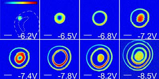
Caption: These images show the electrostatic energy given off when electrons are added to a quantum dot. They were made with an atomic-force microscope.

Credit: Dept. of Physics, McGill University. Usage Restrictions: Contact William Raillant-Clark : 514-398-2189 william.raillant-clark@mcgill.ca.
Although popularly used to connote something very large, the word "quantum" itself actually means the smallest amount by which certain physical quantities can change. Knowledge of these energy levels enables scientists to understand and predict the electronic properties of the nanoscale systems they are developing.

"We are determining optical and electronic transport properties," Grütter said. "This is essential for the development of components that might replace silicon chips in current computers."

The electronic principles of nanosystems also determine their chemical properties, so the team's research is relevant to making chemical processes "greener" and more energy efficient. For example, this technology could be applied to lighting systems, by using nanoparticles to improving their energy efficiency. "We expect this method to have many important applications in fundamental as well as applied research," said Lynda Cockins of McGill's Department of Physics.

The principle of the cantilever sensors sounds relatively simple.
"The cantilever is about 0.5 mm in size (about the thickness of a thumbnail) and is essentially a simple driven, damped harmonic oscillator, mathematically equivalent to a child's swing being pushed," Grütter explained. "The signal we measure is the damping of the cantilever, the equivalent to how hard I have to push the kid on the swing so that she maintains a constant height, or what I would call the 'oscillation amplitude.' "

Dr. Aashish Clerk, Yoichi Miyahara, and Steven D. Bennett of McGill's Dept. of Physics, and scientists at the Institute for Microstructural Sciences of the National Research Council of Canada contributed to this research, which was published online late yesterday afternoon in the Proceedings of the National Academy of Sciences. The research received funding from the Natural Sciences and Engineering Research Council of Canada, le Fonds Québécois de le Recherche sur la Nature et les Technologies, the Carl Reinhardt Fellowship, and the Canadian Institute for Advanced Research. ###

Contact: William Raillant-Clark william.raillant-clark@mcgill.ca 514-398-2189 McGill University

Friday, June 11, 2010

Hot new material can keep electronics cool

Few atomic layers of graphene reveal unique thermal properties.

Professor Alexander Balandin and a team of UC Riverside researchers, including Chun Ning Lau, an associate professor of physics, have taken another step toward new technology that could keep laptops and other electronic devices from overheating.

Balandin, a professor of electrical engineering in the Bourns College of Engineering, experimentally showed in 2008 that graphene, a recently discovered single-atom-thick carbon crystal, is a strong heat conductor. The problem for practical applications was that it is difficult to produce large, high quality single atomic layers of the material.

Now, in a paper published in Nature Materials, Balandin and co-workers found that multiple layers of graphene, which are easier to make, retain the strong heat conducting properties.

Alexander Balandin, University of California - Riverside

Caption: Alexander Balandin is a professor of electrical engineering in the Bourns College of Engineering at the University of California, Riverside.

Credit: UCR Strategic Communications. Usage Restrictions: None.
That's also a significant discovery in fundamental physics. Balandin's group, in addition to measurements, explained theoretically how the materials' ability to conduct heat evolves when one goes from conventional three-dimensional bulk materials to two-dimensional atomically-thin films, such as graphene.

The results published in Nature Materials may have important practical applications in removal of dissipated hear from electronic devices.

Heat is an unavoidable by-product when operating electronic devices. Electronic circuits contain many sources of heat, including millions of transistors and interconnecting wiring. In the past, bigger and bigger fans have been used to keep computer chips cool, which improved performance and extended their life span. However, as computers have become faster and gadgets have gotten smaller and more portable the big-fan solution no longer works.
New approaches to managing heat in electronics include incorporating materials with superior thermal properties, such as graphene, into silicon computer chips. In addition, proposed three-dimension electronics, which use vertical integration of computer chips, would depend on heat removal even more, Balandin said.

Silicon, the most common electronic material, has good electronic properties but not so good thermal properties, particularly when structured at the nanometer scale, Balandin said. As Balandin's research shows, graphene has excellent thermal properties in addition to unique electronic characteristics.

"Graphene is one of the hottest materials right now," said Balandin, who is also chair of the Material Sciences and Engineering program. "Everyone is talking about it."

Graphene is not a replacement for silicon, but, instead could be used in conjunction with silicon, Balandin said. At this point, there is no reliable way to synthesize large quantities of graphene. However, progress is being made and it could be possible in a year or two, Balandin said.

Initially, graphene would likely be used in some niche applications such as thermal interface materials for chip packaging or transparent electrodes in photovoltaic solar cells, Balandin said. But, in five years, he said, it could be used with silicon in computer chips, for example as interconnect wiring or heat spreaders. It may also find applications in ultra-fast transistors for radio frequency communications. Low-noise graphene transistors have already been demonstrated in Balandin's lab.

Balandin published the Nature Materials paper with two of his graduate students Suchismita Ghosh, who is now at Intel Corporation, and Samia Subrina, Lau. one of her graduate students, Wenzhong Bao, and Denis L. Nika and Evghenii P. Pokatilov, visting researchers in Balandin's lab who are based at the State University of Moldova. ###

Contact: Sean Nealon sean.nealon@ucr.edu 951-827-1287 University of California - Riverside

Thursday, June 10, 2010

Rensselaer researchers to send bacteria into orbit aboard space shuttle Atlantis

New study will investigate the effects of microgravity on the formation of biofilms; could lead to safer and healthier space travel.

Troy, N.Y. – A team of researchers from Rensselaer Polytechnic Institute will send an army of microorganisms into space this week, to investigate new ways of preventing the formation and spread of biofilms, or clusters of bacteria, that could pose a threat to the health of astronauts.

The Micro-2 experiment, led by Cynthia Collins, assistant professor in the Department of Chemical and Biological Engineering at Rensselaer, is scheduled to launch into orbit on May 14 aboard Space Shuttle Atlantis.

Micro-2 Flight Patch

Caption: A team of researchers from Rensselaer Polytechnic Institute will send an army of microorganisms into space this week, to investigate new ways of preventing the formation and spread of biofilms, or clusters of bacteria, that could pose a threat to the health of astronauts. The Micro-2 experiment is scheduled to launch into orbit on May 14 aboard Space Shuttle Atlantis. The Micro-2 flight patch is pictured.

Credit: NASA. Usage Restrictions: Please include photo credit.

Researchers from Rensselaer Polytechnic Institute

Caption: A team of researchers from Rensselaer Polytechnic Institute will send an army of microorganisms into space this week, to investigate new ways of preventing the formation and spread of biofilms, or clusters of bacteria, that could pose a threat to the health of astronauts. The Micro-2 experiment is scheduled to launch into orbit on May 14 aboard Space Shuttle Atlantis. Shown are professor and project leader Cynthia Collins (left) with graduate student Jasmine Shong making preparations for the launch of Micro-2.

Credit: Rensselaer/Collins. Usage Restrictions: Please include photo credit.
The microorganisms will spend a week in space before returning to Earth aboard the shuttle. Within just a few hours after the shuttle's return, Collins will be able to examine the bacteria and resulting biofilms to see how their growth and development were impacted by microgravity. The samples also will be returned to Rensselaer, to be examined using the core facilities of the Institute's Center for Biotechnology and Interdisciplinary Studies.

"We know that gravity plays a key role in the development of biological systems, but we don't know exactly how a lack of gravity affects the development of bacteria and biofilms," Collins said. "This means while certain bacteria may be harmless on Earth, they could pose a health threat to astronauts on the International Space Station or, one day, long space flights. Our goal is to better understand how microgravity affects the relationship between humans and bacteria, so we can develop new ways of reduce the threat of biofilms to spacecraft and their crew."

Partnering with Collins on the Micro-2 project are nanobiotechnology expert Jonathan Dordick, the Howard P. Isermann Professor of Chemical and Biological Engineering at Rensselaer and director of the university's Center for Biotechnology and Interdisciplinary Studies, and thin films expert Joel Plawsky, professor in the Department of Chemical and Biological Engineering. NASA is funding the experiment.

Biofilms are complex, three-dimensional microbial communities. Bacteria commonly found in nature are often in the form of biofilms. Most biofilms, including those found in the human body, are harmless. Some biofilms, however, have shown to be associated with disease. Additionally, biofilms in locations such as hospitals – or confined locations like space shuttles – have exhibited resistance to antibiotics. This could pose a problem for astronauts, who have been shown to have an increased susceptibility to infection while in microgravity.
Collins and her team will send up eight devices, called group activation packs (GAPs) and each containing 128 vials of bacteria, aboard the shuttle. While in orbit, astronauts will begin the experiment by manipulating the sealed vials and introducing the bacteria to different membranes. At the same time, Collins will perform the same actions with identical GAPs still on Earth at the Kennedy Space Center in Florida. After the shuttle returns, her team will compare the resulting biofilms to see how the behavior of bacteria and development of biofilms in microgravity differed from the control group. The experiment uses BioServe Space Technologies flight-certified hardware.

The Micro-2 research team will also test if newly developed, nanotechnology-based antimicrobial surfaces – developed by Dordick at Rensselaer – can help slow the growth of biofilms on Earth and in microgravity. If successful, these new antimicrobial surfaces could one day be used in hospitals and spacecraft to help reduce the impact of biofilms on human health. ###
Collins' experiment is the third Rensselaer research project to be launched into space over the past year. In August 2009, an experimental heat transfer system designed by Plawsky and Rensselaer Professor Peter Wayner was installed in the International Space Station (ISS), where it will remain for three years. In November 2009, wear-resistant, low-friction nanomaterials created by Professor Linda Schadler were blasted into orbit aboard Space Shuttle Atlantis, attached to the outer hull of the ISS, and exposed to rigors of space.

Contact: Michael Mullaney, Rensselaer Polytechnic Institute. Troy, NY. 518-276-6161 (office) 518-698-6336 (mobile) mullam@rpi.edu