Thursday, April 29, 2010

Nanotechnologists reveal the frictional characteristics of atomically thin sheets VIDEO

PHILADELPHIA –- A team of nanotechnology researchers from the University of Pennsylvania and Columbia University has used friction force microscopy to determine the nanoscale frictional characteristics of four atomically-thin materials, discovering a universal characteristic for these very different materials. Friction across these thin sheets increases as the number of atomic layers decreases, all the way down to one layer of atoms. This friction increase was surprising as there previously was no theory to predict this behavior.

The finding reveals a significant principle for these materials, which are widely used as solid lubricant films in critical engineering applications and are leading contenders for future nanoscale electronics.


Caption: The movie simulates the process of a tiny tip (with a radius of tens of nanometers, of ~ 10 nm) coming into contact and sliding on suspended elastic thin sheets (with thicknesses of one and four atomic layers respectively), such as graphene or molybdenum disulphide. Because of the attractive interactions between the two surfaces, the thinner sheet snaps on to the tip as it approaches the sample and forms a puckered region.

Credit: University of Pennsylvania and Science. Usage Restrictions: None.

Puckering Effect

Caption: Interatomic forces cause attraction between the atomic sheet and the nano-scale tip of the atomic force microscope. Thin sheets deflect toward the tip, therefore increasing friction. When the tip starts to slide, the sheet deforms further as the deformed area is partially pulled along with the tip. The color scale of the atoms indicates how far the atoms have moved upward (red) or downward (blue) from their original positions. Thicker sheets cannot deflect as easily because they are much stiffer, so the increase in friction is less pronounced, consistent with study measurements.

Credit: University of Pennsylvania and Science. Usage Restrictions: None.
Researchers found that friction progressively increased as the number of layers is reduced on all four materials, regardless of how different the materials may behave chemically, electronically or in bulk quantities. These measurements, supported by computer modeling, suggest that the trend arises from the fact that the thinner a material the more flexible it is, just as a single sheet of paper is much easier to bend than a thick piece of cardboard.

Robert Carpick, professor in the Department of Mechanical Engineering and Applied Mechanics at Penn, and James Hone, professor in the Department of Mechanical Engineering at Columbia, led the project collaboratively.

The team tested the nanotribological, or nano-scale frictional properties, of graphene, molybdenum disulfide (MoS2), hexagonal-BN (h-BN) and niobium diselenide (NbSe2) down to single atomic sheets. The team literally shaved off atomic-scale amounts of each material onto a silicon oxide substrate and compared their findings to the bulk counterparts. Each material exhibited the same basic frictional behavior despite having electronic properties that vary from metallic to semiconducting to insulating.

"We call this mechanism, which leads to higher friction on thinner sheets the 'puckering effect,'" Carpick said. "Interatomic forces, like the van der Waals force, cause attraction between the atomic sheet and the nanoscale tip of the atomic force microscope which measures friction at the nanometer scale."

Because the sheet is so thin — in some samples only an atom thick — it deflects toward the tip, making a puckered shape and increasing the area of interaction between the tip and the sheet, which increases friction. When the tip starts to slide, the sheet deforms further as the deformed area is partially pulled along with the tip, rippling the front edge of the contact area. Thicker sheets cannot deflect as easily because they are much stiffer, so the increase in friction is less pronounced.
The researchers found that the increase in friction could be prevented if the atomic sheets were strongly bound to the substrate. If the materials were deposited onto the flat, high-energy surface of mica, a naturally occurring mineral, the effect goes away. Friction remains the same regardless of the number of layers because the sheets are strongly stuck down onto the mica, and no puckering can occur.

"Nanotechnology examines how materials behave differently as they shrink to the nanometer scale," Hone said. "On a fundamental level, it is exciting to find yet another property that fundamentally changes as a material gets smaller."

The results may also have practical implications for the design of nanomechanical devices that use graphene, which is one of the strongest materials known. It may also help researchers understand the macroscopic behavior of graphite, MoS2 and BN, which are used as common lubricants to reduce friction and wear in machines and devices. ###

The study, published in the current edition of the journal Science, was conducted collaboratively by Carpick and Qunyang Li of the Department of Mechanical Engineering in Penn's School of Engineering and Applied Science; Hone, Changgu Lee and William Kalb of the Department of Mechanical Engineering in the Fu Foundation School of Engineering and Applied Science at Columbia; Xin-Zhou Liu of Leiden University in the Netherlands; and Helmuth Berger of Ecole Polytechnique Fédérale de Lausanne in Switzerland.

Research was funded by the National Science Foundation through Penn's Laboratory for Research into the Structure of Matter, Columbia's Nanoscale Science and Engineering Center, the NSF's Directorate for Engineering, the Defense Advanced Research Projects Agency, the Air Force Office of Scientific Research and the New York State Office of Science, Technology and Academic Research.

Contact: Jordan Reese jreese@upenn.edu 215-573-6604 University of Pennsylvania

Wednesday, April 28, 2010

Carbon Nanostructures—Elixir or Poison?

Los Alamos researchers find a case where size really does matter.

LOS ALAMOS, New Mexico, A Los Alamos National Laboratory toxicologist and a multidisciplinary team of researchers have documented potential cellular damage from “fullerenes”—soccer-ball-shaped, cage-like molecules composed of 60 carbon atoms. The team also noted that this particular type of damage might hold hope for treatment of Parkinson’s disease, Alzheimer’s disease, or even cancer.

The research recently appeared in Toxicology and Applied Pharmacology and represents the first-ever observation of this kind for spherical fullerenes, also known as buckyballs, which take their names from the late Buckminster Fuller because they resemble the geodesic dome concept that he popularized.

Jun Gao

Los Alamos National Laboratory toxicologist Jun Gao works in his laboratory using a protective fume hood. Photo by James R. Rickman
Engineered carbon nanoparticles, which include fullerenes, are increasing in use worldwide. Each buckyball is a skeletal cage of carbon about the size of a virus. They show potential for creating stronger, lighter structures or acting as tiny delivery mechanisms for designer drugs or antibiotics, among other uses. About four to five tons of carbon nanoparticles are manufactured annually.

“Nanomaterials are the 21st century revolution,” said Los Alamos toxicologist Rashi Iyer, the principal research lead and coauthor of the paper. “We are going to have to live with them and deal with them, and the question becomes, ‘How are we going to maximize our use of these materials and minimize their impact on us and the environment?’”
Iyer and lead author Jun Gao, also a Los Alamos toxicologist, exposed cultured human skin cells to several distinct types of buckyballs. The differences in the buckyballs lay in the spatial arrangement of short branches of molecules coming off of the main buckyball structure. One buckyball variation, called the “tris” configuration, had three molecular branches off the main structure on one hemisphere; another variation, called the “hexa” configuration, had six branches off the main structure in a roughly symmetrical arrangement; the last type was a plain buckyball.

The researchers found that cells exposed to the tris configuration underwent premature senescence—what might be described as a state of suspended animation. In other words, the cells did not die as cells normally should, nor did they divide or grow. This arrest of the natural cellular life cycle after exposure to the tris-configured buckyballs may compromise normal organ development, leading to disease within a living organism. In short, the tris buckyballs were toxic to human skin cells.

Moreover, the cells exposed to the tris arrangement caused unique molecular level responses suggesting that tris-fullerenes may potentially interfere with normal immune responses induced by viruses. The team is now pursuing research to determine if cells exposed to this form of fullerenes may be more susceptible to viral infections.

Ironically, the discovery could also lead to a novel treatment strategy for combating several debilitating diseases. In diseases like Parkinson’s or Alzheimer’s, nerve cells die or degenerate to a nonfunctional state. A mechanism to induce senescence in specific nerve cells could delay or eliminate onset of the diseases. Similarly, a disease like cancer, which spreads and thrives through unregulated replication of cancer cells, might be fought through induced senescence. This strategy could stop the cells from dividing and provide doctors with more time to kill the abnormal cells.

Because of the minute size of nanomaterials, the primary hazard associated with them has been potential inhalation—similar to the concern over asbestos exposure.

“Already, from a toxicological point of view, this research is useful because it shows that if you have the choice to use a tris- or a hexa-arrangement for an application involving buckyballs, the hexa-arrangement is probably the better choice,” said Iyer. “These studies may provide guidance for new nanomaterial design and development.”

These results were offshoots from a study (Shreve, Wang, and Iyer) funded to understand the interactions between buckyballs and biological membranes. Los Alamos National Laboratory has taken a proactive role by initiating a nanomaterial bioassessmnet program with the intention of keeping its nanomaterial workers safe while facilitating the discovery of high-function, low-bioimpact nanomaterials with the potential to benefit national security missions. In addition to Gao and Iyer, the LANL program includes Jennifer Hollingsworth, Yi Jiang, Jian Song, Paul Welch, Hsing Lin Wang, Srinivas Iyer, and Gabriel Montano.

Los Alamos National Laboratory researchers will continue to attempt to understand the potential effects of exposure to nanomaterials in much the same way that Los Alamos was a worldwide leader in understanding the effects of radiation during the Lab’s early history. Los Alamos workers using nanomaterials will continue to follow protocols that provide the highest degree of protection from potential exposure.

Meantime, Los Alamos research into nanomaterials provides a cautionary tale for nanomaterial use, as well as early foundations for worker protection. Right now, there are no federal regulations for the use of nanomaterials. Disclosure of use by companies or individuals is voluntary. As nanomaterial use increases, understanding of their potential hazards should also increase.

About Los Alamos National Laboratory

Los Alamos National Laboratory, a multidisciplinary research institution engaged in strategic science on behalf of national security, is operated by Los Alamos National Security, LLC, a team composed of Bechtel National, the University of California, The Babcock & Wilcox Company, and URS for the Department of Energy’s National Nuclear Security Administration.

Los Alamos enhances national security by ensuring the safety and reliability of the U.S. nuclear stockpile, developing technologies to reduce threats from weapons of mass destruction, and solving problems related to energy, environment, infrastructure, health, and global security concerns.

LANL news media contact: James E. Rickman, (505) 665-9203, jamesr@lanl.gov.

Tuesday, April 27, 2010

SuperPower and UH sign high temperature superconducting wire license agreements

The University of Houston (UH) executed two license agreements with SuperPower, a wholly-owned subsidiary of Royal Philips Electronics. One agreement covers the intellectual property on second generation (2G) high temperature superconductor (HTS) wire that is developed under the Sponsored Research Agreement (SRA) previously executed between the two parties. This sponsored research program is led by Venkat Selvamanickam, M.D. Anderson chair professor of mechanical engineering and the director of the Applied Research Hub of the Texas Center for Superconductivity at the University of Houston (TCSUH). The second agreement covers the fundamental composition of matter patent of high temperature superconductor that was discovered by Paul Chu in 1987 at the University of Houston.

High Temperature Superconducting Wire

Caption: This is high temperature superconducting wire developed by UH researcher Venkat Selvmanickam.

Credit: Courtesy of the University of Houston Usage Restrictions: None.
"For the past several years we have partnered closely with the Texas Center for Superconductivity and the University of Houston on our wire development efforts. The execution of both the Sponsored Research Portfolio License Agreement and the Chu Patent License Agreement with the university enables SuperPower to continue to advance in the development of world-class 2G HTS wire for a broad range of applications by providing rights to the basis intellectual property in the field," said Arthur P. Kazanjian, general manager of SuperPower. "The SRA, in particular, further binds the already strong relationship between SuperPower and the university that began when Dr. Selvamanickam joined the university in 2008 and moved from being SuperPower vice president and chief technology officer to the role of chief technology advisor."
Gérard van Spaendonck, senior vice president and chief financial officer, Imaging Systems, Philips Healthcare, added, "the protection afforded SuperPower through these agreements will cover the ongoing SRA development work of SuperPower scientists and university students and staff that is being led by Dr. Selvamanickam. In our drive to get the product into a state of commercial readiness, this work, which fully complements the strong base of intellectual property built by SuperPower over the past ten years, is essential to meeting demanding customer requirements."

"The licensing agreements demonstrate the high value placed by industry on the cutting-edge research at the University of Houston, especially in the energy and medical fields, and is another indication of tier-one quality research that is being conducted by our faculty," said University of Houston President Renu Khator. "We are excited about the opportunity of industry commercializing high temperature superconductor materials and technology that are products of University of Houston research."

The University of Houston and SuperPower are partners in the recently announced $3.5 million Emerging Technology Fund award from the state of Texas to create the Applied Research Hub of TCSUH, as well as in the recently awarded $10.6 million Smart Grid Fault Current Limiting Superconducting Transformer Demonstration program funded by the U.S. Department of Energy. ###

Contact: Melissa Carroll mcarroll@uh.edu 713-743-8153 University of Houston

Monday, April 26, 2010

New path to solar energy via solid-state photovoltaics

A newly discovered path for the conversion of sunlight to electricity could brighten the future for photovoltaic technology. Researchers with Lawrence Berkeley National Laboratory (Berkeley Lab) have found a new mechanism by which the photovoltaic effect can take place in semiconductor thin-films. This new route to energy production overcomes the bandgap voltage limitation that continues to plague conventional solid-state solar cells.

Working with bismuth ferrite, a ceramic made from bismuth, iron and oxygen that is multiferroic – meaning it simultaneously displays both ferroelectric and ferromagnetic properties – the researchers discovered that the photovoltaic effect can spontaneously arise at the nanoscale as a result of the ceramic's rhombohedrally distorted crystal structure.

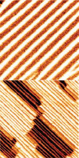
Domain Walls

Caption: These nanoscale images of bismuth ferrite thin films show ordered arrays of 71 degree domain walls (top) and 109 degree doman walls (bottom). By changing the polarization direction of the bismuth ferrite, these domain walls give rise to the photovoltaic effect.

Credit: Image from Seidel, et. al. Usage Restrictions: None.
Furthermore, they demonstrated that the application of an electric field makes it possible to manipulate this crystal structure and thereby control photovoltaic properties.

"We're excited to find functionality that has not been seen before at the nanoscale in a multiferroic material," said Jan Seidel, a physicist who holds joint appointments with Berkeley Lab's Materials Sciences Division and the UC Berkeley Physics Department. "We're now working on transferring this concept to higher efficiency energy-research related devices."

Seidel is one of the lead authors of a paper in the journal Nature Nanotechnology that describes this work titled, "Above-bandgap voltages from ferroelectric photovoltaic devices." Co-authoring this paper with Seidel were Seung-Yeul Yang, Steven Byrnes, Padraic Shafer,Chan-Ho Yang, Marta Rossell, Pu Yu, Ying-Hao Chu, James Scott, Joel Ager, Lane Martin and Ramamoorthy Ramesh.

At the heart of conventional solid-state solar cells is a p-n junction, the interface between a semiconductor layer with an abundance of positively-charged "holes," and a layer with an abundance of negatively charged electrons. When photons from the sun are absorbed, their energy creates electron-hole pairs that can be separated within a "depletion zone," a microscopic region at the p-n junction measuring only a couple of micrometers across, then collected as electricity. For this process to take place, however, the photons have to penetrate the material to the depletion zone and their energy has to precisely match the energy of the semiconductor's electronic bandgap – the gap between its valence and conduction energy bands where no electron states can exist.

"The maximum voltage conventional solid-state photovoltaic devices can produce is equal to the energy of their electronic bandgap," Seidel says.
"Even for so called tandem-cells, in which several semiconductor p-n junctions are stacked, photovoltages are still limited because of the finite penetration depth of light into the material."

Working through Berkeley Lab's Helios Solar Energy Research Center, Seidel and his collaborators discovered that by applying white light to bismuth ferrite, a material that is both ferroelectric and antiferromagnetic, they could generate photovoltages within submicroscopic areas between one and two nanometers across. These photovoltages were significantly higher than bismuth ferrite's electronic bandgap.

"The bandgap energy of the bismuth ferrite is equivalent to 2.7 volts. From our measurements we know that with our mechanism we can get approximately 16 volts over a distance of 200 microns. Furthermore, this voltage is in principle linear scalable, which means that larger distances should lead to higher voltages."

Behind this new mechanism for photovoltage generation are domain walls – two-dimensional sheets that run through a multiferroic and serve as transition zones, separating regions of different ferromagnetic or ferroelectric properties. In their study, Seidel and his collaborators found that these domain walls can serve the same electron-hole separation purpose as depletion zones only with distinct advantages.

"The much smaller scale of these domain walls enables a great many of them to be stacked laterally (sideways) and still be reached by light," Seidel says. "This in turn makes it possible to increase the photovoltage values well above the electronic bandgap of the material."

The photovoltaic effect arises because at the domain walls the polarization direction of the bismuth ferrite changes, which leads to steps in the electrostatic potential. Through annealing treatments of the substrate upon which bismuth ferrite is grown, the material's rhombohedral crystals can be induced to form domain walls that change the direction of electric field polarization by either 71, 109 or 180 degrees. Seidel and his collaborators measured the photovoltages created by the 71 and 109 degree domain walls.

"The 71 degree domain walls showed unidirectional in-plane polarization alignment and produced an aligned series of potential voltage steps," Seidel says. "Although the potential step at the 109 degree domain was higher than the 71 degree domain, it showed two variants of the in-plane polarization which ran in opposite directions."

Seidel and his colleagues were also able to use a 200 volt electric pulse to either reverse the polarity of the photovoltaic effect or turn it off altogether. Such controllability of the photovoltaic effect has never been reported in conventional photovoltaic systems, and it paves the way for new applications in nano-optics and nano-electronics.

"While we have not yet demonstrated these possible new applications and devices, we believe that our research will stimulate concepts and thoughts that are based on this new direction for the photovoltaic effect," Seidel says. ###

Berkeley Lab is a U.S. Department of Energy national laboratory located in Berkeley, California. It conducts unclassified scientific research and is managed by the University of California. Visit our website at www.lbl.gov.

Contact: Lynn Yarris lcyarris@lbl.gov 510-486-5375 DOE/Lawrence Berkeley National Laboratory

Sunday, April 25, 2010

UH Researcher Modernizes U.S. Power Grid

Award-winning materials expert and UH grad returns with SuperPower, Inc

Although the U.S. electric power industry is one of the greatest engineering marvels of the 20th century, aging technology and an increase in demand create problems for the electricity infrastructure that need to be fixed.

Venkat Selvamanickam, director of the Applied Research Hub and the M.D. Anderson chair professor of the department of mechanical engineering, University of Houston, is developing a technology with high temperature superconducting wires that is revolutionizing the way power is generated, transported and used.

Venkat Selvamanickam

Venkat Selvamanickam (center) surrounded by his team of SuperPower researchers who have joined him at the University of Houston.
"The country's electric transmission grid currently consists of about 160,000 miles of high-voltage transmission lines, with forecasters predicting an additional 12,900 miles needed over the next five years to meet increasing demand," said Selvamanickam. "The goal of my research is to modernize the power grid with high temperature superconducting wires to improve efficiency and reliability. Almost anything in the power grid– cables, transformers, motors, generators – can be more efficient if you use high temperature superconducting wires.

Superconducting power cables can transmit up to 10 times more power than traditional copper cables without the significant losses of traditional cables and are considered environmentally friendly. Superconducting fault current limiters can enable uninterrupted power transmission when conventional circuits will otherwise succumb to outages in events such as lightning storms."
On a tour of Selvamanickam's research laboratory at Texas Center for Superconductivity at the University of Houston, he demonstrates different samples of the high temperature superconducting wire that resemble a shiny, metal tape about the size of a hair ribbon, with similar flexibility. The tape has six to eight layers with a ceramic-middle, one-hundredth as thick as human hair, consisting primarily of a coating made from a mixture of yttrium barium copper oxide, generally called YBCO (pronounced IB-co).

High temperature superconductivity defines certain materials like metals and ceramics that lose electrical resistance when cooled by liquid nitrogen, an inexpensive industrial refrigerant that costs less than a bottle of water, a major development in the price point for superconductivity for wide commercial use.

Without this resistance, electrons can travel through these materials freely, leading to wires fabricated into power cables that carry large amounts of electric current for long periods without losing energy as heat. Cooled by liquid nitrogen, high temperature superconducting wires reduce risk of explosion in that it's not flammable.

The applications for high temperature superconducting wire range from advanced medical imaging techniques like magnetic resonance imaging (MRIs) to large-scale applications replacing existing copper wires with superconducting wires to raise reliability and cut costs in electric power transmission and distribution, storage devices, motors, generators, cellular communication systems, to magnetically-levitated trains.

"High temperature superconductivity has the potential to revolutionize the way we use electricity, just like the way fiber-optics revolutionized the way we communicate," said Selvamanickam. "Our research pays immediate returns to the industry. It's not like something that maybe 10 years down the line could be useful."

It is estimated that high-temperature superconducting wires could eliminate 131 million tons of carbon dioxide released into the atmosphere and offset the emission of the equivalent of 40 conventional electricity-generating plants.

Before joining the University of Houston in 2008, Selvamanickam was the chief technology officer at SuperPower. He received his Ph.D. in materials engineering from UH in 1992 and his master's degree in mechanical engineering in 1988. As a graduate student, he created a new method for fabricating high performance superconductors. One of his publications that arose from his master's thesis on superconductivity became one of the most cited works on the subject setting international standards for superconductor performance. He continued the trend of setting world-record performances in superconductor wire in his industrial career at SuperPower.

"SuperPower is one of a handful of companies to develop and manufacture second-generation high temperature superconducting wires in kilometer-long lengths commercially available around the world today. They produce the world's highest-performance wire," said Selvamanickam.

Based in Schenectady, New York, SuperPower signed a research agreement with the University of Houston and is the first partner in the new applied research hub of the Texas Center for Superconductivity at the University of Houston (TCSUH). The company plans to establish a presence in Houston with a specialty products facility at UH's Energy Research Park. Selvamanickam oversees SuperPower's research and development activities from Houston as a chief technical advisor.

In moving its research to the University of Houston, SuperPower transferred to the University unique, thin-film process equipment to make the wire.

"No other university in the country has this kind of equipment. We also have five SuperPower scientists now working out of Houston who also train and mentor graduate students working on the project," said Selvamanickam.

"One reason the University of Houston was selected for its research agreement was its strong commitment to superconductivity research," said University of Houston President Renu Khator. "The Texas Center for Superconductivity houses the largest university-based multidisciplinary research center in the world and is enthusiastic about working with an industry leader like SuperPower."

SuperPower's achievements include demonstrating the world's first integration of high-temperature superconducting wire installed in the grid in upstate New York as part of the Albany Cable Project, a Department of Energy flagship program. SuperPower and Waukesha Electric Systems along working with the University of Houston and Oak Ridge National Laboratory will be installing a fault limiting superconducting transformer in Southern California Edison utility substation, California's largest grid, in 2015.

Selvamanickam attributes his success in the challenging field of superconductivity to being in the right place at the right time as a graduate student at the University of Houston.

"I was at the birthplace of high temperature superconductivity as a graduate student in 1987 at the University of Houston. At the time, Paul Chu, director of the Texas Center for Superconductivity discovered YBCO that broke the liquid nitrogen barrier for superconducting temperature," said Selvamanickam. "I was one of the first researchers to work on the material Chu discovered. We worked around the clock trying to make the material, perform 100 times better. I came up with a new technique to fabricate superconductors and achieved a world record in January 1989 that's still a standard today."

After receiving his degree, Selvamanickan worked at the Oak Ridge National Laboratory for a year as a post-doctoral researcher, then joined Intermagnetics General Corp. In 1996, President Bill Clinton awarded him the Presidential Early Career Achievement Award. He used the $500,000 received from the award as seed money to develop a ground breaking superconducting wire technology at Intermagnetics which was the foundation for the start of SuperPower in 2000. From 2000 to 2008, he built and managed a team of 40+ high-performance personnel and led the company to multiple word firsts including the completion of the world's first significant delivery of second-generation high temperature superconducting wire and multiple world records for superconductor wire performance.

Selvamanickam was named Superconductor Industry Person of the Year in 2005 and his numerous accomplishments in this field are documented with more than 145 papers in several major journals, 30 issued patents and 21 pending U.S. patents, and more than 60 pending international patents.

After nearly 25 years of working in superconductivity, Selvamanickam still finds it a magical phenomenon and is fueled by passion and drive to be a leader in his field.

"There is no theory to explain why these materials are superconducting," Selvamanickam said. "Another thing that gives me goose bumps is there are materials out there that could be superconducting at room temperature, and we don't know it yet."

Contact: Melissa Carroll mcarroll@uh.edu 713-743-8153 University of Houston

Friday, April 23, 2010

Cancer therapy using unique imaging, delivery system focus of NSF CAREER Award

Preliminary research on cancer treatments using nanotechnology and laser therapy has led to a National Science Foundation (NSF) Faculty Early Career Development (CAREER) award for Marissa Nichole Rylander, Virginia Tech assistant professor jointly appointed in the Department of Mechanical Engineering and Virginia Tech – Wake Forest University School of Biomedical Engineering and Sciences (SBES).

The CAREER grant will allow Rylander to develop and utilize a novel sensing system she co-invented called the "holey scaffold." Her design will characterize the three-dimensional and time dependent motion of a nanoparticle used in a treatment process. It will also illustrate the dynamic, light-activated thermal and chemical response of the tumor to the nanoparticle-mediated laser therapy for varying nanoparticle properties and laser parameters within both in vitro and in vivo tumor systems.

Marissa Nichole Rylander, Virginia Tech

aption: Marissa Nichole Rylander, Virginia Tech assistant professor jointly appointed in the Department of Mechanical Engineering and Virginia Tech-Wake Forest University School of Biomedical Engineering and Sciences (SBES), has developed a system capable of minimally invasive and nondestructive light sensitive, molecular sensing and control of biological and transport processes within living organisms.

Credit: Virginia Tech Photo. Usage Restrictions: Photo may be used with discussion of Dr. Rylander's research.
The "holey scaffold" is the first system capable of minimally invasive and non-destructive light sensitive, molecular sensing and control of biological and transport processes within living organisms. Rylander said the "holey scaffold can be visualized as a miniature microscope used in conjunction with a living system. The holey scaffold is built from tissue scaffolding and is embedded with a network of hollow microchannels. Typically made from biodegradable synthetics or biological materials such as collagen, the scaffold promotes tissue growth.

Some microchannels can be used to perform controlled delivery of biological agents (e.g. nutrients, growth factors, tumor cells, nanoparticles, therapeutic agents). Other microchannels can be used to introduce micron size fibers for non-destructive, in situ, and real-time imaging of biological processes or therapeutic light delivery.
Rylander, who joined the Virginia Tech faculty in 2006, earned her doctorate in biomedical engineering from the University of Texas at Austin (UT) in 2005 where she remained as a post doctoral fellow jointly appointed in the biomedical engineering department and Institute for Computational Engineering and Sciences.

Her CAREER award, in part, is a continuation of work at UT on characterization of injury and heat shock protein (HSP) expression in prostate cancer cells and tumors in response to elevated temperatures associated with water bath and laser heating. Knowledge of the HSP expression distribution in tumors allows the identification of tumor regions with a high likelihood of survival and recurrence. Therefore, therapeutic procedures can be modified to optimize HSP expression to enhance treatment outcome.

Based on these experimental measurements she developed novel computational treatment planning models to predict the temperature, HSP expression, and injury at the cellular and tissue level in response to laser therapy. Rylander's goal with her $400,000 CAREER award is to ultimately develop more effective and selective laser cancer therapies by incorporating novel nanoparticles to enhance laser based thermal and chemical treatments.

With her holey scaffold design, she will be able to measure dynamic nanoparticle mass transport, temperature, cell viability, HSP expression, and reactive oxygen species (ROS) production in real-time within an in vitro tumor in a bioreactor or an in vivo tumor within a mouse. She will use a variety of nanoparticles including carbon nanotubes, novel embodiments of carbon nanotubes and fullerenes, and carbon nanohorns in combination with laser irradiation.

By analyzing the tumor's response to varying nanoparticle types, delivery methods, and laser parameters, Rylander expects to be able to create a multi-component, treatment planning computational model for nanoparticle-medicated laser therapy that can be used by clinicians to determine appropriate nanoparticle properties and laser parameters to achieve selective and effective cancer treatment.

Her CAREER award will also allow her to create a course on nanotherapeutics for undergraduates and graduate students. It will explore the basics of nanoparticles, the experimental measurement of nanoparticle interactions with biological tissues, photothermal, and photochemical mechanisms of nanotherapy. The course will also address the computer modeling of cellular and tissue responses to nanoparticles.

This CAREER project will also establish a multi-tier education and outreach plan that will integrate research elements and discoveries into multidisciplinary educational and research experiences for high school students and teachers from underprivileged schools in West Virginia and undergraduates and graduate students at Virginia Tech.

"It is my long-term career goal to be able to develop effective and selective cancer therapies based on nanotechnology that can be readily implemented as a viable treatment option for millions of cancer patients," Rylander said. ###

Contact: Lynn Nystrom tansy@vt.edu
540-231-4371 Virginia Tech

Thursday, April 22, 2010

Scientists discover world's smallest superconductor

Study paves way for development of nanocircuits for energy, electronics applications.

ATHENS, Ohio — Scientists have discovered the world's smallest superconductor, a sheet of four pairs of molecules less than one nanometer wide. The Ohio University-led study, published Sunday as an advance online publication in the journal Nature Nanotechnology, provides the first evidence that nanoscale molecular superconducting wires can be fabricated, which could be used for nanoscale electronic devices and energy applications.

"Researchers have said that it's almost impossible to make nanoscale interconnects using metallic conductors because the resistance increases as the size of wire becomes smaller.

Smallest Superconductor

Caption: This image shows the smallest superconductor, which is only .87 nanometer wide.

Credit: Image courtesy of Saw‑Wai Hla and Kendal Clark, Ohio University. Usage Restrictions: None.
The nanowires become so hot that they can melt and destruct. That issue, Joule heating, has been a major barrier for making nanoscale devices a reality," said lead author Saw-Wai Hla, an associate professor of physics and astronomy with Ohio University's Nanoscale and Quantum Phenomena Institute.

Superconducting materials have an electrical resistance of zero, and so can carry large electrical currents without power dissipation or heat generation. Superconductivity was first discovered in 1911, and until recently, was considered a macroscopic phenomenon.

The current finding suggests, however, that it exists at the molecular scale, which opens up a novel route for studying this phenomenon, Hla said. Superconductors currently are used in applications ranging from supercomputers to brain imaging devices.

In the new study, which was funded by the U.S. Department of Energy, Hla's team examined synthesized molecules of a type of organic salt, (BETS)2-GaCl4, placed on a surface of silver.
Using scanning tunneling spectroscopy, the scientists observed superconductivity in molecular chains of various lengths. For chains below 50 nanometers in length, superconductivity decreased as the chains became shorter. However, the researchers were still able to observe the phenomenon in chains as small as four pairs of molecules, or 3.5 nanometers in length.

To observe superconductivity at this scale, the scientists needed to cool the molecules to a temperature of 10 Kelvin. Warmer temperatures reduced the activity. In future studies, scientists can test different types of materials that might be able to form nanoscale superconducting wires at higher temperatures, Hla said.

"But we've opened up a new way to understand this phenomenon, which could lead to new materials that could be engineered to work at higher temperatures," he said.

The study also is noteworthy for providing evidence that superconducting organic salts can grow on a substrate material.

"This is also vital if one wants to fabricate nanoscale electronic circuits using organic molecules," Hla added. ###

Collaborators on the paper include Kandal Clark, a doctoral student in the Russ College of Engineering and Technology at Ohio University; Sajida Khan, a graduate student in the Department of Physics and Astronomy at Ohio University; Abdou Hassanien, a researcher with the Nanotechnology Research Institute, Advanced Industrial Science and Technology (AIST) and the Japan Science and Technology Agency's Core Research of Evolutional Science & Technology (JST-CREST) in Japan who conducted the work as a visiting scientist at Ohio University; Hisashi Tanaka, a scientist at AIST and JST-CREST who synthesized the molecules; and Kai-Felix Braun, a scientist with the Physikalisch Technische Bundesanstalt in Braunschweig, Germany, who conducted the calculations at the Ohio Supercomputing Center.

Contacts: Saw-Wai Hla, (740) 593-1727, hla@ohio.edu; Director of Research Communications Andrea Gibson, (740) 597-2166, gibsona@ohio.edu.

Contact: Andrea Gibson gibsona@ohio.edu 740-597-2166 Ohio University

Wednesday, April 21, 2010

How immune cells 'sniff out' bacteria

Scientists are learning how our immune system senses and tracks down infection in the body by responding to chemical "scents" emitted by bacteria. Studying how immune cells manipulate their movement in response to external signals could shed light not only on how our immune system functions but also how cancer cells spread through the body and even how the brain wires itself.

Speaking at the Society for General Microbiology's spring meeting in Edinburgh, Dr Holger Kress describes a new technique pioneered by himself and Professor Eric Dufresne at Yale University in the US that uses sponge-like micro-particles to mimic bacteria.

The micro-particles slowly release a characteristic bacterial "scent" that is picked up by immune cells, causing them to actively move towards the source of the chemical in an attempt to hunt down the model microbes.

Stimulating Single Living Cells with Light and Microparticles

Caption: Biophysicists at Yale created a method to stimulate single living cells with light and microparticles. Left side: The five particles pictured are trapped with laser tweezers and release a chemical which attracts the cell. Right side: The cell encounters a larger chemical concentration close to the particles (white-yellow region) than further away from the particles (red-black region).

Credit: Holger Kress and Eric Dufresne. Usage Restrictions: None.
These micro-particles can be trapped and manipulated three-dimensionally using 'optical tweezers' – highly focussed laser beams that are able to precisely control the movement of the particles to within a millionth of a millimetre. "By controlling the shape of the chemical signals, we were able to control the movements of immune cells and study how they respond to the signals," said Dr Kress.

The scientists found that a single chemical-releasing micro-particle was enough to encourage neutrophils (a type of immune cell) to migrate towards it. Within less than one minute's exposure to the micro-particle, the neutrophils were able to polarize the growth of their internal 'skeleton' in the direction of the chemical.
Dr Kress explained that although researchers had successfully identified the types of chemical signals that stimulate immune cells, it is still a challenge to work out the exact details of the immune cell response. "This new technique allows us to measure systematically how cells respond to various stimuli over minute gradients in time and space."

Dr Kress believes his technique could be applied across a wide range of research fields. "Cell migration along chemical gradients of this kind plays a key role in wound healing and the wiring of the brain. It is also an essential feature of many diseases – particularly metastatic cancers," he said. ###

Contact: Laura Udakis l.udakis@sgm.ac.uk 44-118-988-1843 Society for General Microbiology

Tuesday, April 20, 2010

Researchers use improved nanogenerators to power sensors based on zinc oxide nanowires

Self-powered nanosensors: By combining a new generation of piezoelectric nanogenerators with two types of nanowire sensors, researchers have created what are believed to be the first self-powered nanometer-scale sensing devices that draw power from the conversion of mechanical energy. The new devices can measure the pH of liquids or detect the presence of ultraviolet light using electrical current produced from mechanical energy in the environment.

Based on arrays containing as many as 20,000 zinc oxide nanowires in each nanogenerator, the devices can produce up to 1.2 volts of output voltage, and are fabricated with a chemical process designed to facilitate low-cost manufacture on flexible substrates.

Zhong Lin Wang, Georgia Institute of Technology

Caption: Georgia Tech professor Zhong Lin Wang holds an improved nanogenerator containing 700 rows of nanowire arrays. The generator was used to power nanometer-scale sensors.

Credit: Photo: Gary Meek. Usage Restrictions: None.

Nanogenerator Researchers

Caption: Georgia Tech Professor Zhong Lin Wang and researchers Chen Xu and Sheng Xu examine images of nanowire arrays used in their improved nanogenerator.

Credit: Photo: Gary Meek. Usage Restrictions: None.

Nanogenerators/Nanosensors

Caption: This figure shows (a) fabrication of a vertical-nanowire integrated nanogenerator (VING), (b) design of a lateral-nannowire integrated nanogenerator (LING) array, (c) scanning electron microscope image of a row of laterally-grown zinc oxide nanowire arrays, and (d) image of the LING structure.

Credit: Courtesy of Zhong Lin Wang. Usage Restrictions: None.
Tests done with nearly one thousand nanogenerators – which have no mechanical moving parts – showed that they can be operated over time without loss of generating capacity.

Details of the improved nanogenerator and self-powered nanosensors were scheduled to be reported March 28 in the journal Nature Nanotechnology. The research was supported by the National Science Foundation, the Defense Advanced Research Projects Agency, and the U.S. Department of Energy.

"We have demonstrated a robust way to harvest energy and use it for powering nanometer-scale sensors," said Zhong Lin Wang, a Regents professor in the School of Materials Science and Engineering at the Georgia Institute of Technology. "We now have a technology roadmap for scaling these nanogenerators up to make truly practical applications."

For the past five years, Wang's research team has been developing nanoscale generators that use the piezoelectric effect – which produces electrical charges when wires made from zinc oxide are subjected to strain. The strain can be produced by simply flexing the wires, and current from many wires can be constructively combined to power small devices. The research effort has recently focused on increasing the amount of current and voltage generated and on making the devices more robust.

In the paper, Wang and collaborators report on a new configuration for the nanowires that embeds both ends of the tiny structures in a polymer substrate. The wires can then generate current as they are compressed in a flexible nanogenerator enclosure, eliminating the contact with a metallic electrode that was required in earlier devices. Because the generators are completely enclosed, they can be used in a variety of environments.

"We can now grow the wires chemically on substrates that are foldable and flexible and the processing can now be done at substrate temperatures of less than 100 degrees Celsius – about the temperature of coffee," explained Wang. "That will allow lower cost fabrication and growth on just about any substrate."

The nanogenerators are produced using a multi-step process that includes fabrication of electrodes that provide both Ohmic and Shottky contacts for the nanowires. The arrays can be grown both vertically and laterally.
To maximize current and voltage, the growth and assembly requires alignment of crystalline growth, as well as the synchronization of charging and discharging cycles.

Production of vertical nanogenerators begins with growing zinc oxide nanowires on a gold-coated surface using a wet chemical method. A layer of polymethyl-methacrylate is then spun-coated onto the nanowires, covering them from top to bottom. Oxygen plasma etching is then performed, leaving clean tips on which a piece of silicon wafer coated with platinum is placed. The coated silicon provides a Shottky barrier, which is essential for maintaining electrical current flow.

The alternating current output of the nanogenerators depends on the amount of strain applied. "At a strain rate of less than two percent per second, we can produce output voltage of 1.2 volts," said Wang. "The power output is matched with the external load."

Lateral nanogenerators integrating 700 rows of zinc oxide nanowires produced a peak voltage of 1.26 volts at a strain of 0.19 percent. In a separate nanogenerator, vertical integration of three layers of zinc oxide nanowire arrays produced a peak power density of 2.7 milliwatts per cubic centimeter.

Wang's team has so far produced two tiny sensors that are based on zinc oxide nanowires and powered by the nanogenerators. By measuring the amplitude of voltage changes across the device when exposed to different liquids, the pH sensor can measure the acidity of liquids. An ultraviolet nanosensor depends on similar voltage changes to detect when it is struck by ultraviolet light.

In addition to Wang, the team authoring the paper included Sheng Xu, Yong Qin, Chen Xu, Yaguang Wei, and Rusen Wang, all from Georgia Tech's School of Materials Science and Engineering.

The new generator and nanoscale sensors open new possibilities for very small sensing devices that can operate without batteries, powered by mechanical energy harvested from the environment. Energy sources could include the motion of tides, sonic waves, mechanical vibration, the flapping of a flag in the wind, pressure from shoes of a hiker or the movement of clothing.

"Building devices that are small isn't sufficient," Wang noted. "We must also be able to power them in a sustainable way that allows them to be mobile. Using our new nanogenerator, we can put these devices into the environment where they can work independently and sustainably without requiring a battery." ###

Contact: John Toon jtoon@gatech.edu
404-894-6986 Georgia Institute of Technology Research News

Monday, April 19, 2010

Safer nuclear reactors could result from Los Alamos research

Safer nuclear reactors could result from Los Alamos research.

Loading-unloading' effect of grain boundaries key to repair of irradiated metal

Self-repairing materials within nuclear reactors may one day become a reality as a result of research by Los Alamos National Laboratory scientists.

In a paper appearing today in the journal Science, Los Alamos researchers report a surprising mechanism that allows nanocrystalline materials to heal themselves after suffering radiation-induced damage. Nanocrystalline materials are those created from nanosized particles, in this case copper particles.

Safer nuclear reactors A single nanosized particle—called a grain—is the size of a virus or even smaller. Nanocrystalline materials consist of a mixture of grains and the interface between those grains, called grain boundaries.

When designing nuclear reactors or the materials that go into them, one of the key challenges is finding materials that can withstand an outrageously extreme environment. In addition to constant bombardment by radiation, reactor materials may be subjected to extremes in temperature,
physical stress, and corrosive conditions. Exposure to high radiation alone produces significant damage at the nanoscale.

Radiation can cause individual atoms or groups of atoms to be jarred out of place. Each vagrant atom becomes known as an interstitial. The empty space left behind by the displaced atom is known as a vacancy. Consequently, every interstitial created also creates one vacancy. As these defects—the interstitials and vacancies—build up over time in a material, effects such as swelling, hardening or embrittlement can manifest in the material and lead to catastrophic failure.

Therefore, designing materials that can withstand radiation-induced damage is very important for improving the reliability, safety and lifespan of nuclear energy systems.

Because nanocrystalline materials contain a large fraction of grain boundaries—which are thought to act as sinks that absorb and remove defects—scientists have expected that these materials should be more radiation tolerant than their larger-grain counterparts. Nevertheless, the ability to predict the performance of nanocrystalline materials in extreme environments has been severely lacking because specific details of what occurs within solids are very complex and difficult to visualize.

Recent computer simulations by the Los Alamos researchers help explain some of those details.

In the Science paper, the researchers describe the never-before-observed phenomenon of a "loading-unloading" effect at grain boundaries in nanocrystalline materials. This loading-unloading effect allows for effective self-healing of radiation-induced defects. Using three different computer simulation methods, the researchers looked at the interaction between defects and grain boundaries on time scales ranging from picoseconds to microseconds (one-trillionth of a second to one-millionth of a second).

On the shorter timescales, radiation-damaged materials underwent a "loading" process at the grain boundaries, in which interstitial atoms became trapped—or loaded—into the grain boundary. Under these conditions, the subsequent number of accumulated vacancies in the bulk material occurred in amounts much greater than would have occurred in bulk materials in which a boundary didn't exist. After trapping interstitials, the grain boundary later "unloaded" interstitials back into vacancies near the grain boundary. In so doing, the process annihilates both types of defects—healing the material.

This unloading process was totally unexpected because grain boundaries traditionally have been regarded as places that accumulate interstitials, but not as places that release them. Although researchers found that some energy is required for this newly-discovered recombination method to operate, the amount of energy was much lower than the energies required to operate conventional mechanisms—providing an explanation and mechanism for enhanced self-healing of radiation-induced damage.

Modeling of the "loading-unloading" role of grain boundaries helps explain previously observed counterintuitive behavior of irradiated nanocrystalline materials compared to their larger-grained counterparts. The insight provided by this work provides new avenues for further examination of the role of grain boundaries and engineered material interfaces in self-healing of radiation-induced defects. Such efforts could eventually assist or accelerate the design of highly radiation-tolerant materials for the next generation of nuclear energy applications. ###

The Los Alamos National Laboratory research team includes: Xian-Ming Bai, Richard G. Hoagland and Blas P. Uberuaga of the Materials Science and Technology Division; Arthur F. Voter, of the Theoretical Division; and Michael Nastasi of the Materials Physics and Applications Division.

The work was primarily sponsored by the Los Alamos Laboratory-Directed Research and Development (LDRD) program, which, at the discretion of the Laboratory Director, invests a small percentage of the Laboratory's budget in high-risk, potentially high-payoff projects to help position the Laboratory to anticipate and prepare for emerging national security challenges. The research also received specific funding through the Center for Materials under Irradiation and Mechanical Extremes, an Energy Frontier Research Center funded by the U.S. Department of Energy Office of Science, Office of Basic Energy Sciences.

About Los Alamos National Laboratory (www.lanl.gov)

Los Alamos National Laboratory, a multidisciplinary research institution engaged in strategic science on behalf of national security, is operated by Los Alamos National Security, LLC, a team composed of Bechtel National, the University of California, The Babcock & Wilcox Company, and URS for the Department of Energy's National Nuclear Security Administration.

Los Alamos enhances national security by ensuring the safety and reliability of the U.S. nuclear stockpile, developing technologies to reduce threats from weapons of mass destruction, and solving problems related to energy, environment, infrastructure, health, and global security concerns.

Contact: James E. Rickman jamesr@lanl.gov 505-665-9203 DOE/Los Alamos National Laboratory

Sunday, April 18, 2010

Chemist monitors nanotechnology's environmental impact

BINGHAMTON, NY -- Interest in 'green' innovation means not just thinking big but also very, very, very small.

At least that's the way Omowunmi Sadik, director of Binghamton University's Center for Advanced Sensors and Environmental Systems, sees it. She's working to develop sensors that would detect and identify engineered nanoparticles. Her research will advance our understanding of the risks associated with the environmental release and transformation of these particles.

"Society has a duty to not only consider the positive sides of science and technology but also the not-so-desirable sides of technology itself," said Sadik, a professor of chemistry. "We need to think not just about how to make these nanoparticles but also about their impact on human health and the environment."

Omowunmi Sadik, Binghamton University

Caption: Omowunmi Sadik, director of Binghamton University's Center for Advanced Sensors and Environmental Systems, is developing sensors that would detect and identify engineered nanoparticles.

Credit: Jonathan Cohen/Binghamton University. Usage Restrictions: Please contact Binghamton University.
A survey by the Project on Emerging Nanotechnologies found that nanoparticles — particles less than 100 nanometers in size — are now used in more than 1,000 consumer products ranging from cars to food. Silver nanoparticles are widely used as coating materials in cookware and tableware and as ingredients in laundry liquids and clothes because of their antibacterial properties. You can even buy socks infused with silver nanoparticles designed to reduce bacteria and odor.

"But what happens if we buy those socks and we wash them?" Sadik asked. "The nanoparticles end up in our water system."
Little is known about how these and other engineered nanoparticles interact with our water systems, the soil and the air. Some are known toxins; others have properties similar to asbestos. And it's difficult, if not downright impossible, to monitor them. Current techniques rely on huge microscopes to identify nanoparticles, but the devices are not portable and do not provide information about the toxicity of materials.

Sadik and a Binghamton colleague, Howard Wang, have received funding from the Environmental Protection Agency to design, create and test sensors for monitoring engineered nanoparticles and naturally occurring cell particles.

"We need to understand the chemical transformation of these materials in the ecosystem so we can take action to prevent unnecessary exposure," Sadik said. Her lab has already created a membrane that will not only trap a single nanoparticle but also provide a means of signal generation. It uses cyclodextrin, whose molecular structure resembles a tiny cup. "It can be used not only as a sensor, but also for cleanup," Sadik said.

That discovery and others make Sadik believe that nanotechnology may also prove useful in the remediation of environmental pollutants. Green nanotechnology could even reduce the use of solvents and result in manufacturing protocols that produce less waste, she said.

For instance, Sadik has used nanoparticles to transform Chromium 6, a known carcinogen, into Chromium 3, which is benign. "I do see the positive side of it," she said.

"We want to be able to develop nanomaterials while avoiding the unintended consequences of such developments," Sadik added. "We don't want to stop development, but we do want to encourage responsibility." ###

Contact: Gail Glover gglover@binghamton.edu 607-777-2174 Binghamton University

Saturday, April 17, 2010

New tissue-hugging implant maps heart electrical activity in unprecedented detail

Next-generation devices pave way for applications in cardiology, neurology.

PHILADELPHIA – A team of cardiologists, materials scientists, and bioengineers have created and tested a new type of implantable device for measuring the heart's electrical output that they say is a vast improvement over current devices. The new device represents the first use of flexible silicon technology for a medical application.

"We believe that this technology may herald a new generation of active, flexible, implantable devices for applications in many areas of the body," says co-senior author Brian Litt, MD, an associate professor of Neurology at the University of Pennsylvania School of Medicine and also an associate professor of Bioengineering in Penn's School of Engineering and Applied Science.

Tissue-Hugging Implant

Caption: A new type of implantable device uses flexible silicon technology.

Credit: Dae-Hyeong Kim, Ph.D., University of Illinois. Usage Restrictions: None.
"Initially, we plan to apply our findings to the design of devices for localizing and treating abnormal heart rhythms. We believe these new devices will allow doctors to more quickly, safely, and accurately target and destroy abnormal areas of the heart that are responsible for life-threatening cardiac arrhythmias.

"Implantable silicon-based devices have the potential to serve as tools for mapping and treating epileptic seizures, providing more precise control over deep brain stimulation, as well as other neurological applications," says Story Landis, PhD, director of the National Institute of Neurological Disorders and Stroke, which provided support for the study.
"We are excited by the proof of concept evident in the investigators' ability to map cardiac activity in a large animal model."

"The new devices bring electronic circuits right to the tissue, rather than having them located remotely, inside a sealed can that is placed elsewhere in the body, such as under the collar bone or in the abdomen," explains Litt. "This enables the devices to process signals right at the tissues, which allows them to have a much higher number of electrodes for sensing or stimulation than is currently possible in medical devices."

Now, for example, devices for mapping and eliminating life-threatening heart rhythms allow for up to 10 wires in a catheter that is moved in and around the heart, and is connected to rigid silicon circuits distant from the target tissue. This design limits the complexity and resolution of devices since the electronics cannot get wet or touch the target tissue.

The team describes their proof-of-principle findings in the cover article of this week's Science Translational Medicine.

The team tested the new devices – made of nanoscale, flexible ribbons of silicon embedded with 288 electrodes, forming a lattice-like array of hundreds of connections – on the heart of a porcine animal model. The tissue-hugging shape allows for measuring electrical activity with greater resolution in time and space. The new device can also operate when immersed in the body's salty fluids. The devices can collect large amounts of data from the body, at high speed. This allowed the researchers to map electrical activity on the heart of the large animal.

"Our hope is to use this technology for many other kinds of medical applications, for example to treat brain diseases like epilepsy and movement disorders," adds Litt and co-senior author John Rogers, PhD, from the University of Illinois.

In this experiment, the researchers built a device to map waves of electrical activity in the heart of a large animal. The device uses the 288 contacts and more than 2,000 transistors spaced closely together, while standard clinical systems usually use about five to 10 contacts and no active transistors. "We demonstrated high-density maps of electrical activity on the heart recorded from the device, during both natural and paced beats," says co-author David Callans, MD, professor of Medicine at Penn.

"We also plan to design advanced, 'intelligent' pacemakers that can improve the pumping function of hearts weakened by heart attacks and other diseases." For each of these applications, the team is conducting experiments to test flexible devices in animals before starting human trials.

Another focus of ongoing work is to develop similar types of devices that are not only flexible, like a sheet of plastic, but fully stretchable, like a rubber band. The ability to fully conform and wrap around large areas of curved tissues will require stretchability, as well as flexibility. "The next big step in this new generation of implantable devices will be to find a way to move the power source onto them," says Rogers. "We're still working on a solution to that problem."

This research is a result of a collaboration between the Rogers laboratory, where the flexible electronics technology in the devices was developed and fabricated, and Litt's bioengineering laboratory at Penn, where the medical applications were designed and tested. Heart rhythm experiments were designed and performed in Callans' cardiology laboratory. Mechanical engineers Younggang Huang, PhD, and Jianliang Xiao at Northwestern University and University of Illinois performed the mechanical modeling and design that enables the devices to wrap around the heart and other irregular, curved organs. Litt and Rogers note that the core of their collaboration is Penn Bioengineering PhD student Jonathan Viventi and University of Illinois post-doctoral fellow Dae-Hyeong Kim, PhD, who are co-first authors on the publication. The work was also supported by Joshua Moss, MD, a cardiology fellow at Penn, and several undergraduates and master's students. ###

The research was funded by National Institute of Neurological Disorders and Stroke, the Klingenstein Foundation, the Epilepsy Therapy Project, and the University of Pennsylvania Schools of Medicine and Engineering.

This release and a related image can be found at: XX

Penn Medicine is one of the world's leading academic medical centers, dedicated to the related missions of medical education, biomedical research, and excellence in patient care. Penn Medicine consists of the University of Pennsylvania School of Medicine (founded in 1765 as the nation's first medical school) and the University of Pennsylvania Health System, which together form a $3.6 billion enterprise. Penn's School of Medicine is currently ranked #3 in U.S. News & World Report's survey of research-oriented medical schools, and is consistently among the nation's top recipients of funding from the National Institutes of Health, with $367.2 million awarded in the 2008 fiscal year.

Contact: Karen Kreeger karen.kreeger@uphs.upenn.edu 215-349-5658 University of Pennsylvania School of Medicine

Friday, April 16, 2010

Flexible electronics could help put off-beat hearts back on rhythm

Biocompatible electronics could enable new surgical applications.

CHAMPAIGN, Ill. — Arrhythmic hearts soon may beat in time again, with minimal surgical invasion, thanks to flexible electronics technology developed by a team of University of Illinois researchers, in collaboration with the University of Pennsylvania School of Medicine and Northwestern University. These biocompatible silicon devices could mark the beginning of a new wave of surgical electronics.

Co-senior author John Rogers, the Lee J. Flory-Founder Chair in Engineering Innovation and a professor of materials science and engineering at Illinois, and his team will publish their breakthrough in the cover story of the March 24 issue of Science Translational Medicine.

John Rogers, University of Illinois at Urbana-Champaign

Caption: A team of researchers led by John Rogers, the Lee J. Flory-Founder Chair in Engineering at Illinois, have developed biocompatible silicon devices that could mark the beginning of a new wave of surgical electronics.

Credit: Photo by Thompson-McClellan. Usage Restrictions: Credit must be given.
Several treatments are available for hearts that dance to their own tempo, ranging from pacemaker implants to cardiac ablation therapy, a process that selectively targets and destroys clusters of arrhythmic cells. Current techniques require multiple electrodes placed on the tissue in a time-consuming, point-by-point process to construct a patchwork cardiac map. In addition, the difficulty of connecting rigid, flat sensors to soft, curved tissue impedes the electrodes' ability to monitor and stimulate the heart.

Rogers and his team have built a flexible sensor array that can wrap around the heart to map large areas of tissue at once. The array contains 2,016 silicon nanomembrane transistors, each monitoring electricity coursing through a beating heart.
The Pennsylvania team demonstrated the transistor array on the beating hearts of live pigs, a common model for human hearts. They witnessed a high-resolution, real-time display of the pigs' pulsing cardiac tissues – something never before possible.

"We believe that this technology may herald a new generation of devices for localizing and treating abnormal heart rhythms," said co-sernior author Brian Litt, of the University of Pennsylvania.

"This allows us to apply the full power of silicon electronics directly to the tissue," said Rogers, a renowned researcher in the area of flexible, stretchable electronics. As the first class of flexible electronics that can directly integrate with bodily tissues, "these approaches might have the potential to redefine design strategies for advanced surgical devices, implants, prosthetics and more," he said.

The biocompatible circuits – the first ones unperturbed by immersion in the body's salty fluids – represent a culmination of seven years of flexible electronics study by Rogers' group. The researchers build circuits from ultrathin, single-crystal silicon on a flexible or stretchy substrate, like a sheet of plastic or rubber. The nanometer thinness of the silicon layer makes it possible to bend and fold the normally rigid semiconductor.

"If you can create a circuit that's compliant and bendable, you can integrate it very effectively with soft surfaces in the body," such as the irregular, constantly moving curves of the heart, Rogers said.

Collaborations with a theoretical mechanics group at Northwestern University, led by Younggang Huang, yielded important insights into the designs.

The patchwork grid of cardiac sensors adheres to the moist surfaces of the heart on its own, with no need for probes or adhesives, and lifts off easily. The array of hundreds of sensors gives cardiac surgeons a more complete picture of the heart's electrical activity so they can quickly find and fix any short circuits. In fact, the cardiac device boasts the highest transistor resolution of any class of flexible electronics for non-display applications.

The team's next step is to adapt the technology for use with non-invasive catheter procedures, Rogers said. The U. of I. and Pennsylvania teams also are exploring applications for the arrays in neuroscience, applying grids to brain surfaces to study conditions of unusual electrical activity, such as epilepsy.

"It sets out a new design paradigm for interfacing electronics to the human body, with a multitude of possible applications in human health," Rogers said. ###

This work was supported by the U.S. Department of Energy, a National Security Science and Engineering Faculty Fellowship, the National Institutes of Health and the Klingenstein Foundation.

Contact: Liz Ahlberg eahlberg@illinois.edu 217-244-1073 University of Illinois at Urbana-Champaign

Thursday, April 15, 2010

A lab-on-a-chip with moveable channels VIDEO

UC engineering researchers create tiny pools without walls with programmable microfluidic systems.

Microfluidic devices typically depend upon electrokinetic or traditional pressure methods to move microscopic amounts of fluid around a fixed microchip.

As just published as the cover story in "Lab on a Chip," in "Virtual electrowetting channels: electronic liquid transport with continuous channel functionality," engineering researchers at the University of Cincinnati have created a paradigm shift — and moved some tiny channels in the process.


"'Lab on a Chip' is the top journal in the microfluidics community, with an acceptance rate of less than one out of three," says Ian Papautsky, one of the paper's authors.

The field of microfluidics has been intensely investigated for nearly two decades, being traditionally explored within fixed geometries of continuous polymer or glass microchannels. None of the prior approaches was capable of creating any desired channel geometry and being able to keep that channel configuration intact without external stimulus.

With that capability, electrically induced channel functions could bridge the gap between the worlds of programmable droplet and continuous flow microfluidics.

Someone just bridged that "micromoat."

"So here we are working on displays, and creating cutting-edge techniques at moving colored fluids around, and we nearly overlooked the possibilities in lab-on-a-chip or biomedical areas," says Jason Heikenfeld, director of UC's Novel Devices Laboratory and an associate professor of electrical engineering in UC's College of Engineering and Applied Science. Heikenfeld has been making a name for himself — and UC — in the fields of photonics and electrofluidic display technology.

"This is where collaboration comes into play," Heikenfeld continues. "Here at UC we have several internationally known experts in microfluidics and lab-on-a-chip devices. We started collaborating with one of them, Ian Papautsky, and now we find ourselves in the middle of an exciting new application space."

"In microfluidics, we typically work with either continuous flows which give us high throughputs or droplets (digital flows) that can be manipulated electrically," says Papautsky, associate professor of electrical engineering. Papautsky is also director of UC's BioMicroSystems Lab and director of the Micro/Nano Fabrication Engineering Research Center. "In our new collaboration with Jason Heikenfeld, we are merging these two paradigms into a programmable microfluidic system. This is especially exciting because traditionally all lab-on-a-chip devices are limited by the predefined microchannel structure. A programmable microfluidics platform would offer an ability to reconfigure microchannel structure as needed for performing a wide range of biomedical assays, from DNA analysis to immunoassays, on the same chip."

"I am excited to see our work so well received," Papautsky adds ###

Contact: Wendy Beckman wendy.beckman@uc.edu 513-556-1826 University of Cincinnati

Wednesday, April 14, 2010

Incorporating biofunctionality into nanomaterials for medical, health devices

A team led by researchers from North Carolina State University has published a paper that describes the use of a technique called atomic layer deposition to incorporate "biological functionality" into complex nanomaterials, which could lead to a new generation of medical and environmental health applications. For example, the researchers show how the technology can be used to develop effective, low-cost water purification devices that could be used in developing countries.

"Atomic layer deposition is a technique that can be used to create thin films for coating metals or ceramics, and is especially useful for coating complex nanoscale structures," says Dr. Roger Narayan, the paper's lead author. "This paper shows how atomic layer deposition can be used to create biologically functional materials, such as materials that have antibacterial properties.

Coated Nanoporous Alumina Membrane

Caption: This scanning electron micrograph was obtained from a zinc oxide-coated nanoporous alumina membrane.

Credit: Dr. Roger Narayan, North Carolina State University. Usage Restrictions: Image credit must be given.
Another example would be a material that does not bond to proteins in the body, which could be used for implantable medical sensors." Narayan is a professor in the joint biomedical engineering department of NC State's College of Engineering and the University of North Carolina at Chapel Hill.

One of the applications discussed in the paper is a material that could be used as a filter for point-of-use water purification. "This would be very helpful in the developing world, or in disaster situations – like Haiti – where people do not have access to safe water," Narayan says. "Over one billion people do not have access to safe water. This can lead to a variety of public health problems, including cholera and hepatitis."
Specifically, the researchers show that atomic layer deposition can be used to create a film for coating nanoporous membranes, which may be used for filtering out pathogenic bacteria. "The film could also provide antimicrobial functionality," Narayan says, "to neutralize bacteria."

In the study, the researchers found that membranes treated with one of these films were able to neutralize two common pathogens: E. coli and Staphylococcus aureus. The researchers are currently working with colleagues to assess how well the membranes perform against a variety of environmental bacteria. It's anticipated that these membranes could find use in a variety of medical and environmental health applications, such as hemodialysis filters and implantable sensors. ###

The research, "Atomic layer deposition-based functionalization of materials for medical and environmental health applications," is published in the March issue of the journal Philosophical Transactions of the Royal Society A. The research was funded by the National Science Foundation and the National Institutes of Health. The research was co-authored by Narayan, Dr. Nancy Monteiro-Riviere, professor of investigative dermatology and toxicology at the Center for Chemical Toxicology Research and Pharmacokinetics at NC State, Dr. Chunming Jin, a post-doctoral research associate at NC State, and Dr. Junping Zhang, a former post-doctoral research associate at NC State. Additional co-authors were from Kodak Research Laboratories, Argonne National Laboratory, North Dakota State University, National Yang-Ming University in Taiwan, and Taipei Medical University in Taiwan.

Contact: Matt Shipman matt_shipman@ncsu.edu 919-515-6386 North Carolina State University

Tuesday, April 13, 2010

Designer nanomaterials on-demand

Composites are combinations of materials that produce properties inaccessible in any one material. A classic example of a composite is fiberglass - plastic fibers woven with glass to add strength to hockey sticks or the hull of a boat. Unlike the well-established techniques for producing fiberglass and other macroscale composites, however, there aren't general schemes available for making nanoscale composites.

Now, researchers at Berkeley Lab's Molecular Foundry, in collaboration with researcher at the University of California, Berkeley, have shown how nanocomposites with desired properties can be designed and fabricated by first assembling nanocrystals and nanorods coated with short organic molecules, called ligands.

Delia Milliron, DOE/Lawrence Berkeley National Laboratory

Caption: Delia Milliron, of Berkeley Lab’s Molecular Foundry, led the development of a universal method by which designer nanomaterials can be created on-demand.

Credit: Photo by Roy Kaltschmidt, Berkeley Lab Public Affairs. Usage Restrictions: None.
These ligands are then replaced with clusters of metal chalcogenides, such as copper sulfide. As a result, the clusters link to the nanocrystal or nanorod building blocks and help create a stable nanocomposite. The team has applied this scheme to more than 20 different combinations of materials, including close-packed nanocrystal spheres for thermoelectric materials and vertically aligned nanorods for solar cells.

"We're just starting to understand how combining materials on the nanoscale can open up new possibilities for electronic properties and efficient energy technologies," said Delia Milliron, Director of the Inorganic Nanostructures Facility at the Molecular Foundry. "This new process for fabricating inorganic nanocomposites gives us unprecedented ability to tune composition and control morphology."
The researchers anticipate demand from users seeking this latest addition to the Foundry's arsenal of materials synthesis capabilities, as this mix-and-match approach to nanocomposites could be used in an infinite list of applications, including materials for such popular uses as battery electrodes, photovoltaics and electronic data storage.

"The beauty of our method is not just the flexibility of compositions that can be achieved, but the ease with which this can be done. No specialized equipment is required, a variety of substrates can be used and the process is scalable," said Ravisubhash Tangirala, a Foundry post-doctoral researcher working with Milliron. ###

A paper reporting this researcher titled, "Modular inorganic nanocomposites by conversion of nanocrystal superlattices," appears in the journal Angewandte Chemie International Edition and is available in Angewandte Chemie International Edition online. Co-authoring the paper with Milliron and Tangirala were Jessy Baker and Paul Alivisatos.

Portions of this work at the Molecular Foundry were supported by DOE's Office of Science.

The Molecular Foundry is one of the five DOE Nanoscale Science Research Centers (NSRCs), premier national user facilities for interdisciplinary research at the nanoscale. Together the NSRCs comprise a suite of complementary facilities that provide researchers with state-of-the-art capabilities to fabricate, process, characterize and model nanoscale materials, and constitute the largest infrastructure investment of the National Nanotechnology Initiative. The NSRCs are located at DOE's Argonne, Brookhaven, Lawrence Berkeley, Oak Ridge and Sandia and Los Alamos National Laboratories. For more information about the DOE NSRCs, please visit nano.energy.gov.

Berkeley Lab is a U.S. Department of Energy national laboratory located in Berkeley, California. It conducts unclassified scientific research and is managed by the University of California. Visit our website at www.lbl.gov.

Contact: Aditi Risbud asrisbud@lbl.gov
510-486-4861 DOE/Lawrence Berkeley National Laboratory