Saturday, February 27, 2010

Growing cartilage -- no easy task

New nanoscopic material enables cartilage to do what it doesn't do naturally

EVANSTON, Ill. --- Northwestern University researchers are the first to design a bioactive nanomaterial that promotes the growth of new cartilage in vivo and without the use of expensive growth factors. Minimally invasive, the therapy activates the bone marrow stem cells and produces natural cartilage. No conventional therapy can do this.

The results will be published online the week of Feb. 1 by the Proceedings of the National Academy of Sciences (PNAS).

cartilage"Unlike bone, cartilage does not grow back, and therefore clinical strategies to regenerate this tissue are of great interest," said Samuel I. Stupp, senior author, Board of Trustees Professor of Chemistry, Materials Science and Engineering, and Medicine, and director of the Institute for BioNanotechnology in Medicine. Countless people -- amateur athletes, professional athletes and people whose joints have just worn out -- learn this all too well when they bring their bad knees, shoulders and elbows to an orthopaedic surgeon.
Damaged cartilage can lead to joint pain and loss of physical function and eventually to osteoarthritis, a disorder with an estimated economic impact approaching $65 billion in the United States. With an aging and increasingly active population, this figure is expected to grow.

"Cartilage does not regenerate in adults. Once you are fully grown you have all the cartilage you'll ever have," said first author Ramille N. Shah, assistant professor of materials science and engineering at the McCormick School of Engineering and Applied Science and assistant professor of orthopaedic surgery at the Feinberg School of Medicine. Shah is also a resident faculty member at the Institute for BioNanotechnology in Medicine.

Type II collagen is the major protein in articular cartilage, the smooth, white connective tissue that covers the ends of bones where they come together to form joints.

"Our material of nanoscopic fibers stimulates stem cells present in bone marrow to produce cartilage containing type II collagen and repair the damaged joint," Shah said. "A procedure called microfracture is the most common technique currently used by doctors, but it tends to produce a cartilage having predominantly type I collagen which is more like scar tissue."

The Northwestern gel is injected as a liquid to the area of the damaged joint, where it then self-assembles and forms a solid. This extracellular matrix, which mimics what cells usually see, binds by molecular design one of the most important growth factors for the repair and regeneration of cartilage. By keeping the growth factor concentrated and localized, the cartilage cells have the opportunity to regenerate.

Together with Nirav A. Shah, a sports medicine orthopaedic surgeon and former orthopaedic resident at Northwestern, the researchers implanted their nanofiber gel in an animal model with cartilage defects.

The animals were treated with microfracture, where tiny holes are made in the bone beneath the damaged cartilage to create a new blood supply to stimulate the growth of new cartilage. The researchers tested various combinations: microfracture alone; microfracture and the nanofiber gel with growth factor added; and microfracture and the nanofiber gel without growth factor added.

They found their technique produced much better results than the microfracture procedure alone and, more importantly, found that addition of the expensive growth factor was not required to get the best results. Instead, because of the molecular design of the gel material, growth factor already present in the body is enough to regenerate cartilage.

The matrix only needed to be present for a month to produce cartilage growth. The matrix, based on self-assembling molecules known as peptide amphiphiles, biodegrades into nutrients and is replaced by natural cartilage. ###

"The greatest clinical utility of this matrix would be as an adjunct to current minimally invasive surgical techniques," said Nirav Shah, whose practice is based in Palos Heights, Ill. "Our study illustrates the nanofiber gel's excellent potential for accelerating rehabilitation and return to function, improving clinical outcomes, and hopefully delaying, if not stopping, the progression of cartilage lesions into painful degeneration and arthritis."

Further evaluation of the nanomaterial is under way in a larger preclinical study; pending that study's results, clinical trials would be the next step.

The PNAS paper is titled "Supramolecular Design of Self-assembling Nanofibers for Cartilage Regeneration." In addition to Stupp, Ramille Shah and Nirav Shah, other authors of the paper are Marc M. Del Rosario Lim, Caleb Hsieh and Gordon Nuber, all from Northwestern.

Source contacts: Samuel Stupp at 847-491-3002, 312-503-0807 or s-stupp@northwestern.edu and Ramille Shah at 312-503-3931 or ramille-shah@northwestern.edu

Contact: Wendy Leopold w-leopold@northwestern.edu 847-491-4890 Northwestern University

Friday, February 26, 2010

Engineers explore environmental concerns of nanotechnology

Blacksburg, Va. –– As researchers around the world hasten to employ nanotechnology to improve production methods for applications that range from manufacturing materials to creating new pharmaceutical drugs, a separate but equally compelling challenge exists.

History has shown that previous industrial revolutions, such as those involving asbestos and chloroflurocarbons, have had some serious environmental impacts. Might nanotechnology also pose a risk?

Linsey Marr and Peter Vikesland, faculty members in the Via Department of Civil and Environmental Engineering at Virginia Tech, are part of the national Center for the Environmental Implications of NanoTechnology (CEINT), funded by the National Science Foundation (NSF) in 2008.

Peter Vikesland and Linsey Marr, Virginia Tech

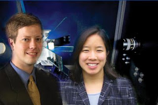
Caption: Peter Vikesland and Linsey Marr, both associate professors of civil and environmental engineering at Virginia Tech, are members of the national Center for the Environmental Implications of NanoTechnology (CEINT) . They are exploring the impact of nanotechnology research on the environment.

Credit: Virginia Tech Photo. Usage Restrictions: This photo may be used with any news or report about Drs Vikesland and Marr's work with CEINT.
Along with Michael Hochella, University Distinguished Professor of Geosciences, they represent Virginia Tech's efforts in a nine-member consortium awarded $14 million over five years, starting in 2008. Virginia Tech's portion is $1.75 million.

CEINT is dedicated to elucidating the relationship between a vast array of nanomaterials — from natural, to manufactured, to those produced incidentally by human activities — and their potential environmental exposure, biological effects, and ecological consequences. It will focus on the fate and transport of natural and manufactured nanomaterials in ecosystems.

Headquartered at Duke University, CEINT is collaboration between Duke, Carnegie Mellon University, Howard University, and Virginia Tech as the core members, as well as investigators from the University of Kentucky and Stanford University.
CEINT academic collaborations in the U.S. also include on-going activities coordinated with faculty at Clemson, North Carolina State, UCLA, and Purdue universities. At Virginia Tech, CEINT is part of the University's Institute for Critical Technology and Applied Science (ICTAS).

Scientists and engineers at the center have outlined plans to conduct research on the possible environmental health impacts of nanomaterials. The plans include new approaches, such as creating a predictive toxicology model based on cell assays and building ecosystems to track nanoparticles.

Characterization of Airborne Particles

In one of the novel ways Marr is conducting her tests, she and her colleagues are growing human lung cells and placing them in chambers that leave the lung cell surface exposed to air. This placement allows for direct contact of the cells with aerosolized particles at the air-liquid interface (ALI). One of Marr's post-doctoral researchers, Amara Holder, and colleagues from Berkeley have previously exposed the cells to particles in diesel exhaust and a methane flame. They compared the ALI exposure to conventional in vitro exposure, where particles are suspended in a liquid cell culture medium.

"Our findings showed the ALI exposure inhalation route is a relevant in vitro approach and is more responsive than the conventional exposure to particle suspensions," they concluded. Now, Marr and her colleagues are repeating the exposure with engineered nanoparticles. The researchers will enhance the deposition of smaller particles by generating an electric field and "relying on the electrophoretic force to drive charged particles to the cell surface."

"With this design, lung cells can be exposed to substantial numbers of aerosolized engineered nanoparticles, such as silver and metal oxides, as single particles rather than large agglomerates," Marr explained. A challenge in tests of nanoparticles' toxicity has been that very small particles like to form aggregates, so testing interactions of the smallest particles with cells requires special approaches.

Marr and one of her graduate students, Andrea Tiwari, have selected the C60 fullerene as a model for carbonaceous nanomaterials because of its relative simplicity, evidence of toxicity, and rich history in the scientific literature. The discovery of the C60 compound in 1985 earned Harold Kroto, James R. Heath, and Richard Smalley the 1996 Nobel Prize in Chemistry. C60 fullerenes and variations on them are being used throughout the nanotechnology industry.

"Airborne carbonaceous nanomaterials are likely to be found in production facilities and in ambient air and may exhibit toxic effects if inhaled," Marr and Tiwari said. They further theorized that when exposed to the air, nanomaterials are likely to be chemically transformed after the exposure to oxidants in the atmosphere.

In their preliminary studies, results indicate that "oxidation does impact solubility, as absorbance after resuspending in water is lower for fullerenes exposed to ozone." The implication is that reactions in the atmosphere can transform nanoparticles and make them more likely to dissolve in water once they deposit back to earth. There, they can travel farther and come in contact with more organisms than if they were stuck to soil.

To collect airborne nanoparticles for analysis, Marr's group designed a low-cost thermophoretic precipitator that uses ice water as a cooling source and a 10-W resistor as the heating source. They flowed synthetic aerosols through the precipitator and used a transmission electron microscope to inspect the particles.

"Preliminary analysis confirmed that this precipitator was effective in collecting nanoparticles of a wide range of sizes and will be effective in future studies of airborne nanoparticles," Marr said.

As her work in this field progresses, Marr was able to use her research in the characterization of airborne particle concentrations during the production of carbonaceous nanomaterials, such as fullerenes and carbon nanotubes, in a commercial nanotechnology facility. Based on the measurements of her study, done with Behnoush Yeganeh, Christy Kull and Mathew Hull, all graduate students, they concluded that engineering controls at the facility "appear to be effective in limiting exposure to nanomaterials," and reported their findings in the American Chemical Society's publication Environmental Science and Technology (Vol. 42, No. 12, 2008)

However, they point to the limitations of this initial study that focused mainly on the physical characterization, and which did not differentiate between particles generated by nanomaterial soot production and those from other sources.

Effects of Carboxylic Acids on nC60 Aggregate Formation

"The increasing production and application of the C60 fullerene due to its distinctive properties will inevitably lead to its release into the environment," Marr's colleague, Vikesland, said. Already, the biomedical, optoelectronics, sensors and cosmetics industries are among the users of the C60 fullerene.

"Little is currently known about the interaction of the C60 fullerene with the constituents of natural waters, and thus it is hard to predict the fate of C60 that is released into the natural environment," Vikesland added. "The C60 fullerene is virtually insoluble in water."

However, one of the components of natural water is natural organic matter (NOM). When the C60 fullerene is released in water, it forms "highly stable dispersed colloidal C60 aggregates or nC60," Vikesland explained. These aggregates can exhibit significant disparities in aggregate structure, size, morphology, and surface charge and behave very differently than the C60 alone.

The problem with NOM is its randomness, resulting in diverse characteristics of the aggregates that form when they mix with the C60.

So, Vikesland is looking at small molecular weight carboxylic acids such as acetic acid, tartaric acid, and citric acid, all widely detected constituents of natural water and biological fluids. He and his graduate student Xiaojun Chang have specifically looked at the formation of nC60 in acetic acid (vinegar) solutions, subjected the aggregates to extended mixing, and found that the solution's chemistry differs substantially from nC60 mixed in water alone.

"The citrate affects the formation of the nC60 in two ways," Vikesland said. It alters the pH, a key factor in controlling the surface charge of nC60 and it directly interacts with the C60 surface.

Vikesland explained the significance of this result. When nC60 is produced in the presence of the carboxylic acids, its aggregates differ significantly from those produced without the acids. In general, Vikesland said, these aggregates have more negative surface charges and are more homogenous than those produced in water alone.

"These results suggest that the ultimate fate of C60 in aqueous environments is likely to be significantly affected by the quantities and types of carboxylic acids present in natural systems and by the solution pH," Vikesland added. Furthermore, because carboxylic acids are common in biological fluids, Vikesland is interested in how his findings relate to the mechanisms by which C60 interact with cells in vivo.

These acids may significantly affect any conclusions ultimately reached regarding the impact of the C60 fullerene into the environment. His current work appears in an issue of Environmental Pollution v157, issue 4 (April 2009), pp. 1072-1080. ###

Contact: Lynn A. Nystrom tansy@vt.edu 540-231-4371 Virginia Tech

Wednesday, February 24, 2010

Energy-harvesting rubber sheets could power pacemakers, mobile phones

Power-generating rubber films developed by Princeton University engineers could harness natural body movements such as breathing and walking to power pacemakers, mobile phones and other electronic devices.

The material, composed of ceramic nanoribbons embedded onto silicone rubber sheets, generates electricity when flexed and is highly efficient at converting mechanical energy to electrical energy. Shoes made of the material may one day harvest the pounding of walking and running to power mobile electrical devices. Placed against the lungs, sheets of the material could use breathing motions to power pacemakers, obviating the current need for surgical replacement of the batteries which power the devices.

Hand-held Power

Caption: Yi Qi, a postdoctoral researcher at Princeton University, holds a piece of silicone rubber imprinted with super-thin material that generates electricity when flexed. The technology could provide a source of power for mobile and medical devices.

Credit: Frank Wojciechowski. Usage Restrictions: For non-commercial use, with credit to Frank Wojciechowski.

Flexible Energy

Caption: The top image shows the process piezoelectric nanoribbons are peeled off a host substrate and placed onto rubber. The middle image is a photograph of the piezo-rubber chip. The bottom image is a schematic of the energy harvesting circuit, which generates power when it's bent.

Credit: Courtesy Michael McAlpine/Princeton University. Usage Restrictions: For non-commercial used, with credit to Michael McAlpine/Princeton University.
A paper on the new material, titled "Piezoelectric Ribbons Printed onto Rubber for Flexible Energy Conversion," was published online Jan. 26, in Nano Letters, a journal of the American Chemical Society. The research was funded by the United States Intelligence Community, a cooperative of federal intelligence and national security agencies.

The Princeton team is the first to successfully combine silicone and nanoribbons of lead zirconate titanate (PZT), a ceramic material that is piezoelectric, meaning it generates an electrical voltage when pressure is applied to it. Of all piezoelectric materials, PZT is the most efficient, able to convert 80% of the mechanical energy applied to it into electrical energy.

"PZT is 100 times more efficient than quartz, another piezoelectric material," said Michael McAlpine, a professor of mechanical and aerospace engineering, at Princeton, who led the project. "You don't generate that much power from walking or breathing, so you want to harness it as efficiently as possible."

The researchers first fabricated PZT nanoribbons – strips so narrow that 100 fit side-by-side in a space of a millimeter. In a separate process, they embedded these ribbons into clear sheets of silicone rubber, creating what they call "piezo-rubber chips." Because the silicone is biocompatible, it is already used for cosmetic implants and medical devices. "The new electricity-harvesting devices could be implanted in the body to perpetually power medical devices, and the body wouldn't reject them," McAlpine said.

In addition to generating electricity when it is flexed, the opposite is true: the material flexes when electrical current is applied to it. This opens the door to other kinds of applications, such as use for microsurgical devices, McAlpine said.

"The beauty of this is that it's scalable," said Yi Qi, a postdoctoral researcher who works with McAlpine. "As we get better at making these chips, we'll be able to make larger and larger sheets of them that will harvest more energy." ###

Qi and McAlpine collaborated with Habib Ahmad of the California Institute of Technology along with Noah Jafferis, a Princeton graduate student in electrical engineering; Kenneth Lyons Jr., an undergraduate at Morehouse College who worked in McAlpine's lab; and Christine Lee, an undergraduate at Princeton.

Contact: Chris Emery cemery@princeton.edu 609-258-4597 Princeton University, Engineering School

Tuesday, February 23, 2010

Mismatched alloys are a good match for thermoelectrics

Employing some of the world's most powerful supercomputers, scientists at Lawrence Berkeley National Laboratory have shown that mismatched alloys are a good match for the future development of high performance thermoelectric devices. Thermoelectrics hold enormous potential for green energy production because of their ability to convert heat into electricity.

Computations performed on "Franklin," a Cray XT4 massively parallel processing system operated by the National Energy Research Scientific Computing Center (NERSC), showed that the introduction of oxygen impurities into a unique class of semiconductors known as highly mismatched alloys (HMAs) can substantially enhance the thermoelectric performance of these materials without the customary degradation in electric conductivity.

Electronic Density of State

Caption: Contour plots showing electronic density of states in HMAs created from zinc selenide by the addition of (a) 3.125-percent oxygen atoms, and (b) 6.25 percent oxygen. The zinc and selenium atoms are shown in light blue and orange. Oxygen atoms (dark blue) are surrounded by high electronic density regions.

Credit: Image provided by Junqiao Wu. Usage Restrictions: None.
"We are predicting a range of inexpensive, abundant, non-toxic materials in which the band structure can be widely tuned for maximal thermoelectric efficiency," says Junqiao Wu, a physicist with Berkeley Lab's Materials Sciences Division and a professor with UC Berkeley's Department of Materials Science and Engineering who led this research.

"Specifically, we've shown that the hybridization of electronic wave functions of alloy constituents in HMAs makes it possible to enhance thermopower without much reduction of electric conductivity, which is not the case for conventional thermoelectric materials," he says.
Collaborating with Wu on this work were Joo-Hyoung Lee and Jeffrey Grossman, both now at the Massachusetts Institute of Technology. The team published a paper on these results in Physical Review Letters titled, "Enhancing the Thermoelectric Power Factor with Highly Mismatched Isoelectronic Doping."

Seebeck Effect and Green Energy
In 1821, the German-Estonian physicist Thomas Johann Seebeck observed that a temperature difference between two ends of a metal bar created an electrical current in between, with the voltage being directly proportional to the temperature difference. This phenomenon became known as the Seebeck thermoelectric effect and it holds great promise for capturing and converting into electricity some of the vast amounts of heat now being lost in the turbine-driven production of electrical power. For this lost heat to be reclaimed, however, thermoelectric efficiency must be significantly improved.

"Good thermoelectric materials should have high thermopower, high electric conductivity, and low thermal conductivity," says Wu. "Enhancement in thermoelectric performance can be achieved by reducing thermal conductivity through nanostructuring. However, increasing performance by increasing thermopower has proven difficult because an increase in thermopower has typically come at the cost of a decrease in electric conductivity."

To get around this conundrum, Wu and his colleagues turned to HMAs, an unusual new class of materials whose development has been led by another physicist with Berkeley Lab's Materials Sciences Division, Wladyslaw Walukiewicz.
Junqiao Wu, DOE/Lawrence Berkeley National Laboratory

Caption: Junqiao Wu, a Berkeley Lab/UC Berkeley physicist, used a NERSC supercomputer to show that the thermoelectric performance of highly mismatched alloys can be substantially enhanced by the introduction of oxygen impurities.

Credit: Photo by Roy Kaltschmidt, Berkeley Lab Public Affairs. Usage Restrictions: None.
HMAs are formed from alloys that are highly mismatched in terms of electronegativity, which is a measurement of their ability to attract electrons. The partial replacement of anions with highly electronegative isoelectronic ions makes it possible to fabricate HMAs whose properties can be dramatically altered with only a small amount of doping. Anions are negatively charged atoms and isoelectronic ions are different elements that have identical electronic configurations.

"In HMAs, the hybridization between extended states of the majority component and localized states of the minority component results in a strong band restructuring, leading to peaks in the electronic density of states and new sub bands in the original band structure," Wu says. "Owing to the extended states hybridized into these sub bands, high electric conductivity is largely maintained in spite of alloy scattering."

In their theoretical work, Wu and his colleagues discovered that this type of electronic structure engineering can be greatly beneficial for thermoelectricity. Working with the semiconductor zinc selenide, they simulated the introduction of two dilute concentrations of oxygen atoms (3.125 and 6.25 percent respectively) to create model HMAs. In both cases, the oxygen impurities were shown to induce peaks in the electronic density of states above the conduction band minimum. It was also shown that charge densities near the density of state peaks were substantially attracted toward the highly electronegative oxygen atoms.

Wu and his colleagues found that for each of the simulation scenarios, the impurity-induced peaks in the electronic density of states resulted in a "sharp increase" of both thermopower and electric conductivity compared to oxygen-free zinc selenide. The increases were by factors of 30 and 180 respectively.

"Furthermore, this effect is found to be absent when the impurity electronegativity matches the host that it substitutes," Wu says. "These results suggest that highly electronegativity-mismatched alloys can be designed for high performance thermoelectric applications."

Wu and his research group are now working to actually synthesize HMAs for physical testing in the laboratory. In addition to capturing energy that is now being wasted, Wu believes that HMA-based thermoelectrics can also be used for solid state cooling, in which a thermoelectric device is used to cool other devices or materials.

"Thermoelectric coolers have advantages over conventional refrigeration technology in that they have no moving parts, need little maintenance, and work at a much smaller spatial scale," Wu says. ###

This project was supported under Berkeley Lab's Laboratory Directed Research and Development Program.

Berkeley Lab is a U.S. Department of Energy national laboratory located in Berkeley, California. It conducts unclassified scientific research for DOE's Office of Science and is managed by the University of California. Visit our Website at www.lbl.gov/

Contact: Lynn Yarris 510-486-5375 DOE/Lawrence Berkeley National Laboratory

Monday, February 22, 2010

Surprising discovery: X-rays drive formation of new crystals

Crystals resemble some biological structures; finding opens door to new technologies

X-rays can do a lot of useful things -- detect broken bones, tumors and dental cavities, analyze atoms in diverse materials and screen luggage at airports -- but who knew they could cause crystals to form?

A team of Northwestern University researchers has discovered that X-rays can trigger the formation of a new type of crystal: charged cylindrical filaments ordered like a bundle of pencils experiencing repulsive forces, which is unknown in crystals. Similar phenomena may occur naturally in biology, such as in the cytoskeleton filaments of cells, which control cell division and migration in cancer metastasis and many other processes.

crystalline bundles of filaments

A network with crystalline bundles of filaments. Photo provided by Yuri S. Velichko.
The results, which were published in the journal Science, expand scientific knowledge of crystals, whether from nature, technological devices or the lab, and also open the door to using X-rays to control the structure of materials or to develop novel biomedical therapies.

Crystal formation is usually based on attractive forces between atoms or molecules, making the Northwestern discovery completely unexpected.

"This is a very intriguing and astonishing result," said Samuel I. Stupp, the paper's senior author and Board of Trustees Professor of Chemistry, Materials Science and Engineering, and Medicine.
"The filaments are charged so one would expect them to repel each other, not to organize into a crystal. Even though they are repelling each other, we believe the hundreds of thousands of filaments in the bundles are trapped within a network and form a crystal to become more stable."

The discovery of the new crystals was serendipitous. Very early one morning at Argonne National Laboratory, the members of Stupp's research team applied synchrotron X-ray radiation to a solution of peptide nanofibers they were studying. (The peptides are small synthetic molecules that can be used to create new materials.) The researchers saw the solution go from clear to opaque.

"There was a dramatic change in the way filaments scattered the radiation," said first author Honggang Cui, a postdoctoral fellow in Stupp's lab. "The X-rays turned a disordered structure into something ordered -- a crystal."

The X-rays increase the charge of the filaments, and thus a repulsive electrostatic force drives the crystallization -- a hexagonal stacking of filaments. Trapped in a three-dimensional network, the charged bundled filaments are unable to escape from each other. The crystals disappear when the X-rays are turned off, and the material is not significantly damaged by the radiation.

As a result of repulsive forces, the filaments are positioned far apart from each other, with as much as 320 angstroms separating the filaments. This striking feature is not found in ordinary crystals where molecules are less than five angstroms apart.

"There are oceans of water inside the crystal," Stupp said. "More than 99 percent of the structure is water." The researchers also observed that when the concentration of the charged filaments in solution was higher, the same crystals formed spontaneously without the need to expose them to X-rays. ###

The Science paper is titled "Spontaneous and X-Ray Triggered Crystallization at Long Range in Self-Assembling Filament Networks." In addition to Stupp and Cui, other authors of the paper are E. Thomas Pashuck, Yuri S. Velichko, Steven

Contact: Megan Fellman fellman@northwestern.edu 847-491-3115 Northwestern University

Neuron connections seen in 3-D

A team of researchers from the Max Planck Institute of Biochemistry, in Germany, led by the Spanish physicist Rubén Fernández-Busnadiego, has managed to obtain 3D images of the vesicles and filaments involved in communication between neurons. The method is based on a novel technique in electron microscopy, which cools cells so quickly that their biological structures can be frozen while fully active.

"We used electron cryotomography, a new technique in microscopy based on ultra-fast freezing of cells, in order to study and obtain three-dimensional images of synapsis, the cellular structure in which the communication between neurons takes place in the brains of mammals" Rubén Fernández-Busnadiego, lead author of the study which features on the front cover of this month's Journal of Cell Biology and a physicist at the Max Planck Institute of Biochemistry, in Germany, tells SINC.

3-D Synapses

Caption: This three-dimensional visualization of synapses shows the tomography mail synaptic vesicles (yellow), cell membrane (purple), connectors between vesicles (red), filaments that anchor the vesicles to the cell membrane (blue), microtubule (dark green), material synaptic space (light green) and postsynaptic density (orange).

Credit: Fernández-Busnadiego et al. Usage Restrictions: None
During synapsis, a presynaptic cell (emitter) releases neurotransmitters to another post-synaptic one (recipient), generating an electric impulse in it, thereby allowing nervous information to be transmitted. During this study, the researchers focused on the tiny vesicles (measuring around 40 nanometres in diameter), which transport and release the neurotransmitters from the presynaptic terminals.

"Thanks to the use of certain pharmacological treatments and the advanced 3D imaging analysis method we have developed, it is possible to observe the huge range of filamentous structures that are within the presynaptic terminal and interact directly with the synaptic vesicles, as well as to learn about their crucial role in responding to the electrical activity of the brain," explains Fernández-Busnadiego.
The filaments connect the vesicles and also connect them with the active area, the part of the cellular membrane from which the neurotransmitters are released. According to the Spanish physicist, these filamentous structures act as barriers that block the free movement of the vesicles, keeping them in their place until the electric impulse arrives, as well as determining the ease with which they will fuse with the membrane.

Sub-zero images

The technique upon which these discoveries are based, electron cryotomography, makes it possible to obtain three-dimensional images of the inside of cells and to minimise any changes to their structure. This is possible because the cells are not fixed with chemical reagents, but are vitrified – in other words they are frozen so fast that the water inside them does not have time to crystallise, and remains in solid state.

These samples, which are always maintained at liquid nitrogen temperatures (below -140 ºC), can be viewed using specially-equipped microscopes. In addition, this method does not require any kind of additional staining, meaning the density of the biological structures can be observed directly. ###

References:

Rubén Fernández-Busnadiego, Benoît Zuber, Ulrike Elisabeth Maurer, Marek Cyrklaff, Wolfgang Baumeister y Vladan Lučić. "Quantitative analysis of the native presynaptic cytomatrix by cryoelectron tomography". The Journal of Cell Biology 188 (1):145-156, 11 de enero de 2010.

Contact: SINC info@plataformasinc.es 34-914-251-820 FECYT - Spanish Foundation for Science and Technology

Sunday, February 21, 2010

Watching crystals grow provides clues to making smoother, defect-free thin films

To make thin films for semiconductors in electronic devices, layers of atoms must be grown in neat, crystalline sheets. But while some materials grow smooth crystals, others tend to develop bumps and defects – a serious problem for thin-film manufacturing.

In the online edition of the journal Science (Jan. 22, 2010), Cornell researchers shed new light on how atoms arrange themselves into thin films. Led by assistant professor of physics Itai Cohen, they recreated conditions of layer-by-layer crystalline growth using particles much bigger than atoms, but still small enough that they behave like atoms.


Movie of colloidal particles forming a crystal. The movie is sped up by about a factor of 100. tai Cohen group.

thin films for semiconductors

Four images from different points in time during an island growth experiment. tai Cohen group.

thin films for semiconductors

Schematic of atoms diffusing on and near a crystal island. The green particles are encountering an edge or corner, where they find a barrier. The orange particle encounters smaller barriers as it moves from site to site. The 1 indicates the bond being broken. The 2 indicates a bond that is forming. Near an edge or corner, the atoms do not have a new neighbor to form a bond with, which is what creates the barrier. Itai Cohen group
"These particles are big and slow enough that you can see what's going on in real time," explained graduate student Mark Buckley. Using an optical microscope, the scientists could watch exactly what their "atoms" – actually, micron-sized silica particles suspended in fluid – did as they crystallized. What's more, they were able to manipulate single particles one at a time and test conditions that lead to smooth crystal growth. In doing so, they discovered that the random darting motion of the particles is a key factor that affects how the crystals grow.

A major challenge to growing thin films with atoms is that the atoms often form mounds, rather than crystallizing into thin sheets. This happens because as atoms are deposited onto a substrate, they initially form small crystals, called islands. When more atoms are dumped on top of these crystals, the atoms tend to stay atop the islands, rather than hopping off the edges - as though there were a barrier on the crystals' edges. This creates the pesky rough spots, "and it's game over" for a perfect thin film, Cohen said.

Conventional theory says that atoms that land on top of islands feel an energetic "pull" from other atoms that keeps them from rolling off. In their colloidal system, the researchers eliminated this pull by shortening the bonds between their particles. But they still saw that their particles hesitated at the islands' edges.

Further analysis using optical tweezers that manipulated individual particles allowed the researchers to measure just how long it took for particles to move off the crystal islands. Because the particles were suspended in a fluid, they were knocked about in what's called Brownian motion, which is like a random walk.

As the particles moved and diffused from one area to another, the researchers noted that the distance a particle had to travel to "fall" off an island's edge was three times farther than moving laterally from one site on the island to another.

And because the particles had to go this distance in a Brownian fashion, it took them nine times longer to complete this "fall." This difference in time explained why the researchers still saw a barrier at their island edges.

Atoms on a crystalline film move in a manner similar to Brownian particles, since the vibrations of the underlying crystal, called phonons, tend to jostle them about. The researchers surmised that in addition to the bonding between the atoms, this random motion may also contribute to the barrier at the crystals' edges, and hence the roughness in the crystal film.
"If the principles we have uncovered can be applied to the atomic scale, scientists will be able to better control the growth of thin films used to manufacture electronic components for our computers and cell phones," Cohen said. ###

The paper's co-authors are former postdoctoral associate Rajesh Ganapathy, now a faculty member at the Jawaharlal Nehru Centre for Advanced Scientific Research in Bangalore, India, and Sharon Gerbode and Mark Buckley, both graduate students.

The work was funded by King Abdullah University of Science and Technology, the Cornell Center for Materials Research, the National Science Foundation and the Cornell Nanoscale Science and Technology Facility.

Contact: Blaine Friedlander bpf2@cornell.edu 607-254-8093 Cornell University

Turning down the noise in quantum data storage

A roundabout method of reading data can improve quantum memory.

Researchers who hope to create quantum computers are currently investigating various methods to store data. Nitrogen atoms embedded in diamond show promise for encoding quantum bits (qubits), but the process of reading the information results in an extremely weak signal. Now physicists have demonstrated a roundabout approach for generating a significantly stronger signal from these sorts of qubits. Their experiment is reported in the current issue of Physical Review B and highlighted with a Viewpoint in the January 19 issue of Physics (http://physics.aps.org.)

In a quantum computer, a single bit of information is encoded into a property of a quantum mechanical system—the spin of an electron, for example.

Roundabout Quantum Data Read-out

Caption: Driving a qubit along a longer quantum path (routes 2 and 3) dramatically improves the signal quality over that achieved by following the shorter path (route 1). The research applies to information stored in qubits that consisted of Nitrogen-based defects in diamond, as schematically shown on the right.

Credit: Alan Stonebraker. Usage Restrictions: None.
In most arrangements that rely on Nitrogen atoms in diamond to store data, reading the information also resets the qubit, which means there is only one opportunity to measure the state of the qubit. By developing a technique that involves the spin of the Nitrogen nucleus in the process as well, a team of physicists at the University of Stuttgart in Germany has turned the single step read-out into a multi-step process.
Rather than simply resetting the electron-based qubit when the information is read, the researchers discovered that they can force the state of the Nitrogen nucleus to change state twice before the information in the qubit is finally erased. The state of the Nitrogen nucleus doesn't store any useful information, it simply allows the researchers to add steps to the process of reading the qubit's state. This results in a more convoluted quantum mechanical process that triples the number of events that occur before information is destroyed, which in turn strengthens the signal revealing information stored in the qubit.

The resulting signal is still weak, but by combining other clever methods to the problem researchers might one day be able to use impurities in diamond to read and write quantum information at room temperature—which would bring us much closer to creating practical quantum computers. ###

Contact: James Riordon riordon@aps.org 301-209-3238 American Physical Society

Friday, February 19, 2010

Breakthrough breast cancer therapy reduces mastectomies, saves breast

Heat treatment with chemotherapy kills large tumors; Approved by FDA; Next stage clinical trials start this year at OUHSC

OKLAHOMA CITY – A new treatment developed and tested by University of Oklahoma researchers not only killed large breast cancer tumors, but reduced the need for mastectomies by almost 90 percent. The latest results appear in an upcoming issue of the Annals of Surgical Oncology.

Building on this success, researchers at the OU Health Sciences Center, plan to start the next phase of clinical trials this year to test the therapy on even larger tumors.

William C. Dooley, M.D., University of Oklahoma

Caption: William Dooley, M.D., OU Cancer Institute, is leading a team of researchers across the United States in the use of microwaves with chemotherapy to kill larger tumors in breast cancer.

Credit: OU Medicine. Usage Restrictions: None.
"This therapy is a major advancement for women with later stage breast cancer. Right now, most patients with large tumors lose their breast. With this treatment along with chemotherapy, we were able to kill the cancer and save the breast tissue," said William Dooley, M.D., a researcher at the OU Cancer Institute and the director of surgical oncology at OU Medicine.

Dr. Dooley is leading a group of researchers from OU, the Massachusetts Institute of Technology, the Los Angeles Biomedical Research Institute, the Comprehensive Breast Center in Florida and St. Joseph's Hospital in California.

They are working on a treatment called Focused Microwave Thermotherapy. The technique, which was approved by the U.S. Food and Drug Administration, uses a modified version of the microwave technology behind the "Star Wars" defense system.

In the most recent study, researchers tested the therapy on tumors that were an inch to an inch and a half in size.
These large tumors usually require mastectomies. When researchers used the heating therapy within two hours of patients receiving chemotherapy, the tumor was more susceptible to the chemotherapy and shrunk rapidly. The percentage of patients needing mastectomies was reduced from 75 percent to 7 percent.

"The trial was very successful. We were able to completely reverse those odds," Dooley said. "We redesigned the machine and will begin clinical trials this year to determine whether the therapy works on tumors that are larger than one and a half inches and smaller than 5 inches in size."

In theory, Dooley said the technique could be used on any organ that could be "held relatively still." Scientists are now working to integrate heat-sensitive nanotechnology that would more precisely target cancer cells. They also plan to study a byproduct of the rapid disintegration of the tumor – a boosted immune system. Dooley said it looks like the rapid release of cancer proteins into the blood stream is causing an immune response that could reduce the chance of cancer recurrence. ###

As Oklahoma's only comprehensive academic cancer center, the OU Cancer Institute is raising the standard of cancer treatment in the state through research and education. The center is working toward an application to the National Cancer Institute to be designated as a "Comprehensive Cancer Center," the gold standard of cancer research and care. Later this year, the OU Cancer Institute will move into a new 210,000-square-foot building. The facility will bring all outpatient cancer programs under one roof at the University of Oklahoma Health Sciences Center. For additional Information, visit www.OUCancer.org.

Contact: Diane Clay diane-clay@ouhsc.edu 405-271-2323 University of Oklahoma

European collaboration breakthrough in developing graphene

A collaborative research project has brought the world a step closer to producing a new material on which future nanotechnology could be based. Researchers across Europe, including the UK's National Physical Laboratory (NPL), have demonstrated how an incredible material, graphene, could hold the key to the future of high-speed electronics, such as micro-chips and touchscreen technology.

Graphene has long shown potential, but has previously only been produced on a very small scale, limiting how well it could be measured, understood and developed. A paper published on the 17th January, in Nature Nanotechnology explains how researchers have, for the first time, produced graphene to a size and quality where it can be practically developed, and successfully measured its electrical characteristics. These significant breakthroughs overcome two of the biggest barriers to scaling up the technology.

A technology for the future

Graphene, only one atom thick

Graphene, only one atom thick, climbs terraces on the surface of a silicone carbide substrate. This picture of a graphene device was taken with an atomic force microscope by NPL's Dr Olga Kazakova
Graphene is a relatively new form of carbon made up of a single layer of atoms arranged in a honeycomb shaped lattice. Despite being one atom thick and chemically simple, graphene's is extremely strong and highly conductive, making it ideal for high-speed electronics, photonics and beyond.

Graphene is a strong candidate to replace semiconductor chips. Moore's Law observes that the density of transistors on an integrated circuit doubles every two years, but silicon and other existing transistor materials are thought to be close to the minimum size where they can remain effective. Graphene transistors can potentially run at faster speeds and cope with higher temperatures. Graphene could be the solution to ensuring computing technology to continue to grow in power whilst shrinking in size, extending the life of Moore's law by many years.
Large microchip manufacturers such as IBM and Intel have openly expressed interest in the potential of graphene as a material on which future computing could be based.

Graphene also has potential for exciting new innovations such as touchscreen technology, LCD displays and solar cells. Its unparalleled strength and transparency make it perfect for these applications, and its conductivity would offers a dramatic increase in efficiency on existing materials.

Growing to a usable size while maintaining quality

Until now graphene of sufficient quality has only been produced in the form of small flakes of tiny fractions of a millimeter, using painstaking methods such as peeling layers off graphite crystals with sticky tape. Producing useable electronics requires much larger areas of material to be grown. This project saw researchers, for the first time, produce and successfully operate a large number of electronic devices from a sizable area of graphene layers (approximately 50 mm2).

The graphene sample, was produced epitaxially - a process of growing one crystal layer on another - on silicon carbide. Having such a significant sample not only proves that it can be done in a practical, scalable way, but also allowed the scientists to better understand important properties.

Measuring resistance

The second key breakthrough of the project was measuring graphene's electrical characteristics with unprecedented precision, paving the way for convenient and accurate standards to be established. For products such as transistors in computers to work effectively and be commercially viable, manufacturers must be able to make such measurements with incredible accuracy against an agreed international standard.

The international standard for electrical resistance is provided by the Quantum Hall Effect, a phenomenon whereby electrical properties in 2D materials can be determined based only on fundamental constants of nature.

The effect has, until now, only been demonstrated with sufficient precision in a small number of conventional semiconductors. Furthermore, such measurements need temperatures close to absolute zero, combined with very strong magnetic fields, and only a few specialised laboratories in the world can achieve these conditions.

Graphene was long tipped to provide an even better standard, but samples were inadequate to prove this. By producing samples of sufficient size and quality, and accurately demonstrate Hall resistance, the team proved that graphene has the potential to supersede conventional semiconductors on a mass scale.

Furthermore graphene shows the Quantum Hall Effect at much higher temperatures. This means the graphene resistance standard could be used much more widely as more labs can achieve the conditions required for its use. In addition to its advantages of operating speed and durability, this would also speed the production and reduce costs of future electronics technology based on graphene

Prof Alexander Tzalenchuk from NPL's Quantum Detection Group and the lead author on the Nature Nanotechnology paper observes: "It is truly sensational that a large area of epitaxial graphene demonstrated not only structural continuity, but also the degree of perfection required for precise electrical measurements on par with conventional semiconductors with a much longer development history."

Where now?

The research team isn't content to leave it there. They are hoping to go on to demonstrate even more precise measurement, as well as accurate measurement at even higher temperatures. They are currently seeking EU funding to drive this forward.

Dr JT Janssen, an NPL Fellow who worked on the project, said: "We've laid the groundwork for the future of graphene production, and will strive in our ongoing research to provide greater understanding of this exciting material. The challenge for industry in the coming years will be to scale the material up in a practical way to meet new technology demands. We have taken a huge step forward, and once the manufacturing processes are in place, we hope graphene will offer the world a faster and cheaper alternative to conventional semiconductors". ###

The research was a joint project carried by the National Physical Laboratory; Chalmers University of Technology, Göteborg, Sweden; Politecnico di Milano, Italy; Linköping University, Sweden and Lancaster University, UK. Measurement was carried out by the Quantum Detection Group at the UK's at the National Physical Laboratory, Teddington, UK.

Technical detail

The sample was grown epitaxially by removing all silicon atoms in a controlled way from a single surface layer of silicon carbide and allowing the remaining carbon to form the nearly ideal graphene monolayer. The next step was to use standard microfabrication techniques, such as the electron beam lithography and reactive ion etching, to produce devices ranging in lateral size from a few micrometers (1 micrometer = 0.001 mm) to hundreds of micrometers and still only one carbon atom thick. All devices measured so far showed the desired electronic characteristics.

The Quantum Hall Effect

This appears where an electric current flows through a two dimensional material in a perpendicular magnetic field and the voltage in the material is measured perpendicular to both the current flow and the field. Within certain periodic intervals of field, the ratio of this transverse voltage to the current, known as the Hall resistance, is determined only by a known combination of fundamental constants of nature – the Planck's constant h and the electron charge e.

Because of this universality, the Quantum Hall effect provides the basis for the resistance standard in principle independent of a particular sample, material or measurement setup.

The Quantum Hall effect has, until now, only been accurately demonstrated with sufficient precision in a small number of conventional semiconductors, such as Si and group III-V heterostructures. Because of its unique electronic structure, graphene was long tipped to provide an even better standard, but the small size of graphene flakes and insufficient quality of early graphene films did not allow accurate measurements to be performed.

About NPL

The National Physical Laboratory (NPL) is one of the UK's leading science facilities and research centres. It is a world-leading centre of excellence in developing and applying the most accurate standards, science and technology available.

NPL occupies a unique position as the UK's National Measurement Institute and sits at the intersection between scientific discovery and real world application. Its expertise and original research have underpinned quality of life, innovation and competitiveness for UK citizens and business for more than a century.

Notes to Editors The Nature Paper Can be viewed here dx.doi.org/10.1038/NNANO.2009.474

Contact: David Lewis david@proofcommunication.com 084-568-01865 National Physical Laboratory

Thursday, February 18, 2010

New nanoparticles target cardiovascular disease

Could potentially eliminate need for arterial stents in some patients

CAMBRIDGE, Mass. — Researchers at MIT and Harvard Medical School have built targeted nanoparticles that can cling to artery walls and slowly release medicine, an advance that potentially provides an alternative to drug-releasing stents in some patients with cardiovascular disease.

The particles, dubbed "nanoburrs" because they are coated with tiny protein fragments that allow them to stick to target proteins, can be designed to release their drug payload over several days. They are one of the first such particles that can precisely home in on damaged vascular tissue, says Omid Farokhzad, associate professor at Harvard Medical School and an author of a paper describing the nanoparticles in the Jan. 18 issue of the Proceedings of the National Academy of Sciences.

Farokhzad and MIT Institute Professor Robert Langer, also an author of the paper, have previously developed nanoparticles that seek out and destroy tumors.

nanoburrs

nanoburrs
The nanoburrs are targeted to a specific structure, known as the basement membrane, which lines the arterial walls and is only exposed when those walls are damaged. Therefore, the nanoburrs could be used to deliver drugs to treat atherosclerosis and other inflammatory cardiovascular diseases. In the current study, the team used paclitaxel, a drug that inhibits cell division and helps prevent the growth of scar tissue that can clog arteries.
"This is a very exciting example of nanotechnology and cell targeting in action that I hope will have broad ramifications," says Langer.

The researchers hope the particles could become a complementary approach that can be used with vascular stents, which are the standard of care for most cases of clogged and damaged arteries, or in lieu of stents in areas not well suited to them, such as near a fork in the artery.

The particles, which are spheres 60 nanometers in diameter, consist of three layers: an inner core containing a complex of the drug and a polymer chain called PLA; a middle layer of soybean lecithin, a fatty material; and an outer coating of a polymer called PEG, which protects the particle as it travels through the bloodstream.

The drug can only be released when it detaches from the PLA polymer chain, which occurs gradually by a reaction called ester hydrolysis. The longer the polymer chain, the longer this process takes, so the researchers can control the timing of the drug's release by altering the chain length. So far, they have achieved drug release over 12 days, in tests in cultured cells.

In tests in rats, the researchers showed that the nanoburrs can be injected intravenously into the tail and still reach their intended target — damaged walls of the left carotid artery. The burrs bound to the damaged walls at twice the rate of nontargeted nanoparticles.

Because the particles can deliver drugs over a longer period of time, and can be injected intravenously, patients would not have to endure repeated and surgically invasive injections directly into the area that requires treatment, says Juliana Chan, a graduate student in Langer's lab and lead author of the paper.

How they did it: The researchers screened a library of short peptide sequences to find one that binds most effectively to molecules on the surface of the basement membrane. They used the most effective one, a seven-amino-acid sequence dubbed C11, to coat the outer layer of their nanoparticles.

Next steps: The team is testing the nanoburrs in rats over a two-week period to determine the most effective dose for treating damaged vascular tissue. The particles may also prove useful in delivering drugs to tumors.

"This technology could have broad applications across other important diseases, including cancer and inflammatory diseases where vascular permeability or vascular damage is commonly observed," says Farokhzad. ###

Source: "Spatiotemporal controlled delivery of nanoparticles to injured vasculature," Juliana Chan, Liangfang Zhang, Rong Tong, Debuyati Ghosh, Weiwei Gao, Grace Liao, Kai Yuet, David Gray, June-Wha Rhee, Jianjun Cheng, Gershon Golomb, Peter Libby, Robert Langer, Omid Farokhzad. Proceedings of the National Academy of Sciences, week of Jan. 18, 2010.

Contact: Jen Hirsch jfhirsch@mit.edu 617-253-1682 Massachusetts Institute of Technology

Wednesday, February 17, 2010

Iowa State researchers part of $78 million national effort to develop advanced biofuels

AMES, Iowa – Two teams of Iowa State University researchers will receive a total of $8 million over three years from a $78 million U.S. Department of Energy program to research and develop advanced biofuels.

Victor Lin – professor of chemistry, director of the Institute for Physical Research and Technology's Center for Catalysis at Iowa State and chief technologist and founder of Catilin Inc. – will lead a team embarking on a $5.3 million study of biodiesel production from algae.

And Robert C. Brown – an Anson Marston Distinguished Professor in Engineering, the Gary and Donna Hoover Chair in Mechanical Engineering and the Iowa Farm Bureau director of the Bioeconomy Institute – will lead a $2.7 million study of the thermochemical and catalytic conversion of biomass to fuels.

Victor Lin, Iowa State University

Caption: Victor Lin will lead a $5.3 million study of biodiesel production from algae using silica nanoparticles.

Credit: By Bob Elbert/Iowa State University. Usage Restrictions: None.
"These grants to Iowa State University researchers demonstrate the breadth and strength of our programs in advanced biofuels," said Sharron Quisenberry, Iowa State's vice president for research and economic development. "We have researchers who can help this national effort to develop clean, sustainable and cost-effective sources of energy. These grants are two more examples of how Iowa State translates discoveries into viable technologies and products that strengthen the economies of Iowa and the world."
The Iowa State research projects are part of a Department of Energy effort supported by the American Recovery and Reinvestment Act. The program creates two national research groups charged with finding ways to break down barriers to the commercialization of advanced biofuels (such as green gasoline) while using the existing fuel marketing and transportation infrastructure:

* $44 million (plus $11 million in non-federal, cost-share funding) creates the National Alliance for Advanced Biofuels and Bioproducts led by the Donald Danforth Plant Science Center in St. Louis, Mo.

* And $34 million (plus $8.4 million in non-federal, cost-share funding) creates the National Advanced Biofuels Consortium led by the National Renewable Energy Laboratory in Golden, Colo., and the Pacific Northwest National Laboratory in Richland, Wash.

Lin's research team is part of the National Alliance for Advanced Biofuels and Bioproducts. It includes researchers at Catilin Inc., a catalyst technology company that Lin founded in 2007 with the help of Mohr Davidow Ventures of Menlo Park, Calif.

The researchers will study how silica nanoparticles developed by Lin – and produced by Ames-based Catilin Inc. – can be used to selectively extract and sequester fuel-related, high-value compounds from a mixture containing lipids from algae. The rest of the algal oil will be converted to biodiesel using Catilin's commercially available T300 catalyst.

"Our technology is instrumental in several key steps of the algae-to-biofuels supply chain as the efficient oil-extraction and solid catalyst provides a cost effective conversion route," Lin said.

Brown's research team is part of the National Advanced Biofuels Consortium. It includes Brent Shanks, the director of the Center for Biorenewable Chemicals based at Iowa State and professor of chemical and biological engineering; James Dumesic, Steenbock Professor of chemical and biological engineering at the University of Wisconsin-Madison; and Linda Broadbelt, professor and chair of chemical and biological engineering at Northwestern University in Evanston, Ill.

The researchers will investigate the chemical reactions of fast pyrolysis (a process that uses heat in the absence of oxygen to decompose biomass into a liquid bio-oil). They'll also study the catalytic upgrading of bio-oil to transportation fuels.

"The Department of Energy organized these consortia for the purpose of accelerating the development of advanced biofuels through a coordinated research program among biofuels researchers across the United States," said Brown. "We are pleased that the Bioeconomy Institute was selected to be part of this national effort."

The national research effort is aimed at building a domestic bio-industry, creating jobs and reducing the country's dependence on foreign oil, according to Steven Chu, the U.S. secretary of energy.

"Advanced biofuels are crucial to building a clean energy economy," Chu said. "By harnessing the power of science and technology, we can bring new biofuels to market and develop a cleaner and more sustainable transportation sector." ###

Contact: Victor Lin vsylin@iastate.edu 515-294-3135 Iowa State University

Tuesday, February 16, 2010

Harnessing the divas of the nanoworld

Michigan Tech scientist grows nano-fields of BNNTs

Boron nitride nanotubes (BNNTs) are the divas of the nanoworld. In possession of alluring properties, they are also notoriously temperamental compared to their carbon-based cousins.

On the plus side, they can withstand incredibly high heat, well over 1,100 degrees Celsius, says Yoke Khin Yap, an associate professor of physics at Michigan Technological University. "Carbon nanotubes would burn like charcoal in a barbecue at half of those temperatures," he says. And the electrical properties of BNNTs are remarkably uniform.

Boron Nitride Nanotubes

Caption: These are carpets of boron nitride nanotubes grown on a substrate by Yoke Khin Yap's research group at Michigan Technological University.

Credit: Yoke Khin Yap. Usage Restrictions: None.
Perfect insulators, boron nitride nanotubes could be doped with other materials to form designer semiconductors that could be used in high-powered electronics.

Unfortunately, making nanotubes from boron and nitrogen is easier said than done. "Making carbon nanotubes is simpler, like cooking," says Yap. Boron nitride nanotubes, on the other hand, have always been fussy, requiring special instrumentation, dangerous chemistry, or temperatures of over 1,500 degrees Celsius to assemble. Even at that, the products are shot through with impurities.
"We've been stuck for more than 10 years because nobody could grow them well on substrates," says Yap. "But now we can."

As it turns out, boron nitride nanotubes just needed a little encouragement. Yap and his team have grown virtual Persian carpets of the tiny fibers on a substrate made from simple catalysts, magnesium oxide, iron or nickel. And they have managed it using the same instrumentation for growing carbon nanotubes, at about 1,100 degrees Celsius. And, their quality is perfect,.the present work. "I hope this encourages more researchers to grow BNNTs using the new technique," said Yap.

The boron nitride nanotubes can be made to assemble exclusively on these catalysts, so the researchers can control precisely where they grow. "You could write 'Michigan Tech' in nanotubes," says Yap.

These transparent nanotube sheets have another interesting property: they shed water like a duck's back, a quality known as the lotus effect. "Water just slides away," he says. "Anything coated with it would not only be stain resistant, it would be protected from anything water-soluble." This superhydrophobicity holds at all pH levels, so anything coated with it would be protected from even the strongest acids and alkalies. ###

The research was funded through a National Science Foundation Career Grant. A paper detailing Yap's discoveries, "Patterned Growth of Boron Nitride Nanotubes by Catalytic Chemical Vapor Deposition," has been published online by the journal Chemistry of Materials.

Yap is the editor of the book "B-C-N Nanotubes and Related Nanostructures," the first book on nanostructures constructed from one or multiple elements using boron, carbon, and nitrogen. He was the lead organizer of the Nanotubes and Related Nanostructures Symposium at the 2009 Materials Research Society Fall Meeting on. For more information, visit www.phy.mtu.edu/yap/research .

Michigan Technological University (mtu.edu) is a leading public research university developing new technologies and preparing students to create the future for a prosperous and sustainable world. Michigan Tech offers more than 130 undergraduate and graduate degree programs in engineering; forest resources; computing; technology; business; economics; natural, physical and environmental sciences; arts; humanities; and social sciences.

Contact: Marcia Goodrich mlgoodri@mtu.edu 906-487-2343 Michigan Technological University

Monday, February 15, 2010

Nanoscience goes 'big'

UCSD nanoengineering discovery could lead to enhanced electronics.

Nanoscience has the potential to play an enormous role in enhancing a range of products, including sensors, photovoltaics and consumer electronics. Scientists in this field have created a multitude of nano scale materials, such as metal nanocrystals, carbon nanotubes and semiconducting nanowires. However, despite their appeal, it has remained an astounding challenge to engineer the orientation and placement of these materials into the desired device architectures that are reproducible in high yields and at low costs – until now. Jen Cha, a UC San Diego nanoengineering professor, and her team of researchers, have discovered that one way to bridge this gap is to use biomolecules, such as DNA and proteins. Details of this discovery were recently published in a paper titled "Large Area Spatially Ordered Arrays of Gold Nanoparticles Directed by Lithographically Confined DNA Origami," in Nature Nanotechology.

Jen Cha

Caption: Jen Cha, a UC San Diego nanoengineering professor, is pushing the envelop in nanoscience by using biology to engineer the assembly of nanoscale materials for applications in medicine, electronics and energy.

Credit: UC San Diego. Usage Restrictions: Credit UC San Diego.

Albert Hung

Caption: Albert Hung, a UCSD nanoengineering post doc, aided in a recent discovery that could lead to enhanced sensors and electronics using nano materials.

Credit: UC San Diego. Usage Restrictions: None.
"Self-assembled structures are often too small and affordable lithographic patterns are too large," said Albert Hung, lead author of the Nature Nanotechnology paper and a post doc working in Cha's lab. "But rationally designed synthetic DNA nanostructures allow us to access length scales between 5 and 100 nanometers and bridge the two systems.

"People have created a huge variety of unique and functional nanostructures, but for some intended applications they are worthless unless you can place individual structures, billions or trillions of them at the same time, at precise locations," Hung added. "We hope that our research brings us a step closer to solving this very difficult problem."

Hung said the recently discovered method may be useful for fabricating nanoscale electronic or optical circuits and multiplex sensors.

"A number of groups have worked on parts of this research problem before, but to our knowledge, we're the first to attempt to address so many parts together as a whole," he said.

One of the main applications of this research that Cha and her group are interested in is for sensing. "There is no foreseeable route to be able to build a complex array of different nanoscale sensing elements currently," said Cha, a former IBM research scientist who joined the UCSD Jacobs School of Engineering faculty in 2008. "Our work is one of the first clear examples of how you can merge top down lithography with bottom up self assembly to build such an array. That means that you have a substrate that is patterned by conventional lithography, and then you need to take that pattern and merge it with something that can direct the assembly of even smaller objects, such as those having dimensions between 2 and 20 nanometers. You need an intermediate template, which is the DNA origami, which has the ability to bind to something else much smaller and direct their assembly into the desired configuration. This means we can potentially build transistors from carbon nanotubes and also possibly use nanostructures to detect certain proteins in solutions. Scientists have been talking about patterning different sets of proteins on a substrate and now we have the ability to do that."

Cha said the next step would be to actually develop a device based on this research method.

"I'm very interested in the applications of this research and we're working our way to get there," she said.
For the last 6 years, Cha's research has focused on using biology to engineer the assembly of nanoscale materials for applications in medicine, electronics and energy. One of the limitations of nanoscience is it doesn't allow mass production of products, but Cha's work is focused on trying figure out how to do that and do it cheaply. Much of her recent work has focused on using DNA to build 2D structures.

"Using DNA to assemble materials is an area that many people are excited about," Cha said. "You can fold DNA into anything you want – for example, you can build a large scaffold and within that you could assemble very small objects such as nano particles, nano wires or proteins.

"Engineers need to understand the physical forces needed to build functional arrays from functional materials," she added. "My job as a nanoengineer is to figure out what you need to do to put all the different parts together, whether it's a drug delivery vehicle, photovoltaic applications, sensors or transistors. We need to think about ways to take all the nano materials and engineer them it into something people can use and hold." ###

Large-area spatially ordered arrays of gold nanoparticles directed by lithographically confined DNA origami, Nature Nanotechnology, Albert M. Hung, Christine M. Micheel, Luisa D. Bozano, Lucas W. Osterbur, Greg M. Wallraff2 & Jennifer N. Cha

Contact: Andrea Siedsma asiedsma@soe.ucsd.edu 858-822-0899 University of California - San Diego

Sunday, February 14, 2010

UCLA's California NanoSystems Institute welcomes new start-up to incubator space

Aneeve to develop sensors to monitor hormone levels for menopause, fertility

Aneeve Nanotechnologies LLC has been selected to work in the UCLA on-campus Technology Incubator Program at the California NanoSystems Institute. The startup company will conduct early-stage research for the development of a novel hormone sensor/meter for biomedical applications in the areas of infertility and menopause.

Aneeve has licensed related carbon nanotube technology from UCLA developed by Kang Wang, a UCLA professor of electrical engineering. The technology increases hormonal detection sensitivity significantly, allowing detection beyond traditional sensors.

Kang Wang

UCLA Engineering professor Kang Wang, Photo credit: I. Fertik
The company is using this technology to develop biomedical applications that are low in power consumption and small in size and that involve ultra-sensitive nanoelectronic technologies.

Aneeve's primary research focus within the incubator will be to develop a consumer-based, simple-to-use meter for sensing estrogen and progesterone hormone levels to assist women in mitigating unwanted symptoms of menopause.
The meter will provide on-demand hormonal levels so patients can better control drug intake related to hormone therapy. The system is intended to be low cost, compact and easy to use. Currently, there is no such meter commercially available.

The sensor and transducer technology will measure hormone concentrations using specially made hormone tabs — similar to the glucose tabs used by diabetics — made by low-cost and precise ink-jet printing of carbon nanotubes. Additionally, the device will allow couples to monitor hormone patterns to help increase chances of fertility, especially among those seeking infertility treatments.

Aneeve's scientific advisory committee includes Kang Wang, who holds the Raytheon Chair in Physical Science at UCLA and is a University of California Distinguished Professor in Electrical Engineering; Wang is a pioneering scientist and technologist who brings vast experience in charge-based nanodevices. The committee also includes University of Southern California professor Chongwu Zhou, who holds joint appointments within the USC College departments of physics and chemistry and has extensive experience in carbon nanotube fabrication, devices and carbon nanotube-on-insulator technology.

"After speaking with medical experts at UCLA and USC, our research collaborators recognized a real need for a simple non-invasive device," said Wang, upon whose technology the license is based. "Such consumer-based meters for on-demand sensing of estrogen and progesterone concentrations are not currently available."

As a startup in the UCLA incubator, Aneeve will benefit from close access to the core facilities within CNSI. In developing the hormone sensor, the company plans to make extensive use of such labs as the Center for Quantum Research, the Nano and Pico Characterization lab, the Electron Imaging Center for Nanomachines, the Integrated Nanomaterials Lab and the Integrated Systems Nanofabrication Cleanroom.

"Aneeve's proof-of-concept work will be greatly aided by access to cutting-edge lab equipment and technical expertise at the incubator," Zhou said. "This will propel the research and development efforts significantly and help Aneeve to get to market that much faster." ###

The California NanoSystems Institute at UCLA is an integrated research center operating jointly at UCLA and UC Santa Barbara whose mission is to foster interdisciplinary collaborations for discoveries in nanosystems and nanotechnology; train the next generation of scientists, educators and technology leaders; and facilitate partnerships with industry, fueling economic development and the social well-being of California, the United States and the world.

The CNSI was established in 2000 with $100 million from the state of California and an additional $250 million in federal research grants and industry funding. At the institute, scientists in the areas of biology, chemistry, biochemistry, physics, mathematics, computational science and engineering are measuring, modifying and manipulating the building blocks of our world — atoms and molecules. These scientists benefit from an integrated laboratory culture enabling them to conduct dynamic research at the nanoscale, leading to significant breakthroughs in the areas of health, energy, the environment and information technology.

Contact: Jennifer Marcus jmarcus@cnsi.ucla.edu 310-267-4839 University of California - Los Angeles

Friday, February 12, 2010

Brandeis wins $1 million Keck Foundation grant to research active matter

active matter

Model indicating how microtubles (blue and green), molecular motors (red) and cross-links (black) generate motion.
Researchers exploit biology to make advances in soft matter physics.

Brandeis University announced today a $1 million, three-year award from the W.M. Keck Foundation to help support experimental research into a new category of materials known as active matter. The project seeks to elucidate the behavior of active matter at length scales ranging from the microscopic to the macroscopic.

Unlike inert materials such as steel or plastic, active matter can move on its own, displaying properties previously observed only in living materials such as muscles and cells.
The project will leverage the university’s pioneering, interdisciplinary approach to research at the intersection of biology and physics. Last year, Brandeis joined an elite group of universities when it won a highly-competitive $7.8 million grant from the National Science Foundation to begin interdisciplinary research on active matter

“Brandeis has been at the forefront of recent advances in materials science and biology, both in studying the properties of materials occurring in biological systems, and in understanding the role of material properties in the structure and function of cells and cellular components,” said principal investigator Seth Fraden, an expert on colloidal liquid crystals and microfluidics.

Many biological systems display self-organized and distinctive dynamic states at the macroscale—think flocking birds, schooling fish, or swarming bacteria. Similarly, at the mesoscale, cellular motility, and at the microscale or sub-cellular level, cytoskeletal reorganization, represent distinctive dynamic states. All these systems are examples of active matter: they consume energy to generate movement, or stress, in space or time.

“In this project, we will exploit biology in order to make advances in active matter, which has become a frontier field in soft matter physics,” said physicist Zvonimir Dogic, who uses optical microscopy to study self-assembly of biopolymers. “In return, our understanding of non-equilibrium phenomena and active materials will shed new light on a number of important biological structures that are not under direct genetic control, such as flagella beating.”

Along with Dogic and Fraden, the research team includes biologist Daniela Nicastro, a leading authority on high-resolution electron tomography. The project uses two complimentary approaches towards studies of active matter. In a “top-down” approach the researchers will systematically deconstruct fully functioning biological organelles to determine the minimal set of components required for active behavior. In a complimentary “bottom-up” approach they will put well-defined isolated components together in a predefined structure and study how active behavior emerges from spontaneous interactions of the constituent molecules.

Historically, basic research on liquids, colloids, polymers and other soft materials has had spectacular consequences for technology, with liquid crystal displays being the prime example, said Fraden. “We believe that this research has great potential for technological development.”

About Brandeis University

Characterized by academic excellence since its founding in 1948, Brandeis is one of the country’s youngest private research universities and the only nonsectarian Jewish-sponsored college or university in the nation. Named for late U.S. Supreme Court Justice Louis D. Brandeis, Brandeis combines the faculty and resources of a world-class research institution with the intimacy and personal attention of a small liberal arts college.

About the W.M. Keck Foundation

Based in Los Angeles, the W. M. Keck Foundation was established in 1954 by the late W. M. Keck, founder of the Superior Oil Company. The Foundation’s grant making is focused primarily on pioneering efforts in the areas of medical research, science and engineering. The Foundation also maintains a program to support undergraduate science and humanities education and a Southern California Grant Program that provides support in the areas of health care, civic and community services, education and the arts, with a special emphasis on children.

Contact: Laura Gardner gardner@brandeis.edu 781-736-4204 Brandeis University