Sunday, January 31, 2010

Glitter-sized solar photovoltaics produce competitive results

Adventures in microsolar supported by microelectronics and MEMS techniques.

ALBUQUERQUE, N.M. — Sandia National Laboratories scientists have developed tiny glitter-sized photovoltaic cells that could revolutionize the way solar energy is collected and used.

The tiny cells could turn a person into a walking solar battery charger if they were fastened to flexible substrates molded around unusual shapes, such as clothing.

The solar particles, fabricated of crystalline silicon, hold the potential for a variety of new applications. They are expected eventually to be less expensive and have greater efficiencies than current photovoltaic collectors that are pieced together with 6-inch- square solar wafers.

Representative Thin Crystalline-Silicon Photovoltaic Cells

Caption: These are representative thin crystalline-silicon photovoltaic cells -- these are from 14 to 20 micrometers thick and 0.25 to 1 millimeter across.

Credit: Murat Okandan. Usage Restrictions: News and educational use.

Greg Nielson, DOE/Sandia National Laboratories

Caption: Sandia project lead Greg Nielson holds a solar cell test prototype with a microscale lens array fastened above it. Together, the cell and lens help create a concentrated photovoltaic unit.

Credit: Randy Montoya. Usage Restrictions: educational and news use.

From left to right, Sandia researchers Murat Okandan, Greg Nielson, and Jose Luis Cruz-Campa

Caption: From left to right, Sandia researchers Murat Okandan, Greg Nielson, and Jose Luis Cruz-Campa, hold samples containing arrays of microsolar cells.

Credit: Randy Montoya. Usage Restrictions: news and educational use.
The cells are fabricated using microelectronic and microelectromechanical systems (MEMS) techniques common to today's electronic foundries.

Sandia lead investigator Greg Nielson said the research team has identified more than 20 benefits of scale for its microphotovoltaic cells. These include new applications, improved performance, potential for reduced costs and higher efficiencies.

"Eventually units could be mass-produced and wrapped around unusual shapes for building-integrated solar, tents and maybe even clothing," he said. This would make it possible for hunters, hikers or military personnel in the field to recharge batteries for phones, cameras and other electronic devices as they walk or rest.

Even better, such microengineered panels could have circuits imprinted that would help perform other functions customarily left to large-scale construction with its attendant need for field construction design and permits.

Said Sandia field engineer Vipin Gupta, "Photovoltaic modules made from these microsized cells for the rooftops of homes and warehouses could have intelligent controls, inverters and even storage built in at the chip level. Such an integrated module could greatly simplify the cumbersome design, bid, permit and grid integration process that our solar technical assistance teams see in the field all the time."

For large-scale power generation, said Sandia researcher Murat Okandan, "One of the biggest scale benefits is a significant reduction in manufacturing and installation costs compared with current PV techniques."

Part of the potential cost reduction comes about because microcells require relatively little material to form well-controlled and highly efficient devices.

From 14 to 20 micrometers thick (a human hair is approximately 70 micrometers thick), they are 10 times thinner than conventional 6-inch-by-6-inch brick-sized cells, yet perform at about the same efficiency.

100 times less silicon generates same amount of electricity
"So they use 100 times less silicon to generate the same amount of electricity," said Okandan. "Since they are much smaller and have fewer mechanical deformations for a given environment than the conventional cells, they may also be more reliable over the long term."

Another manufacturing convenience is that the cells, because they are only hundreds of micrometers in diameter, can be fabricated from commercial wafers of any size, including today's 300-millimeter (12-inch) diameter wafers and future 450-millimeter (18-inch) wafers. Further, if one cell proves defective in manufacture, the rest still can be harvested, while if a brick-sized unit goes bad, the entire wafer may be unusable. Also, brick-sized units fabricated larger than the conventional 6-inch-by-6-inch cross section to take advantage of larger wafer size would require thicker power lines to harvest the increased power, creating more cost and possibly shading the wafer. That problem does not exist with the small-cell approach and its individualized wiring.

Other unique features are available because the cells are so small. "The shade tolerance of our units to overhead obstructions is better than conventional PV panels," said Nielson, "because portions of our units not in shade will keep sending out electricity where a partially shaded conventional panel may turn off entirely."

Because flexible substrates can be easily fabricated, high-efficiency PV for ubiquitous solar power becomes more feasible, said Okandan.

A commercial move to microscale PV cells would be a dramatic change from conventional silicon PV modules composed of arrays of 6-inch-by-6-inch wafers. However, by bringing in techniques normally used in MEMS, electronics and the light-emitting diode (LED) industries (for additional work involving gallium arsenide instead of silicon), the change to small cells should be relatively straightforward, Gupta said.

Each cell is formed on silicon wafers, etched and then released inexpensively in hexagonal shapes, with electrical contacts prefabricated on each piece, by borrowing techniques from integrated circuits and MEMS.

Offering a run for their money to conventional large wafers of crystalline silicon, electricity presently can be harvested from the Sandia-created cells with 14.9 percent efficiency. Off-the-shelf commercial modules range from 13 to 20 percent efficient.

A widely used commercial tool called a pick-and-place machine — the current standard for the mass assembly of electronics — can place up to 130,000 pieces of glitter per hour at electrical contact points preestablished on the substrate; the placement takes place at cooler temperatures. The cost is approximately one-tenth of a cent per piece with the number of cells per module determined by the level of optical concentration and the size of the die, likely to be in the 10,000 to 50,000 cell per square meter range. An alternate technology, still at the lab-bench stage, involves self-assembly of the parts at even lower costs.

Solar concentrators — low-cost, prefabricated, optically efficient microlens arrays — can be placed directly over each glitter-sized cell to increase the number of photons arriving to be converted via the photovoltaic effect into electrons. The small cell size means that cheaper and more efficient short focal length microlens arrays can be fabricated for this purpose.

High-voltage output is possible directly from the modules because of the large number of cells in the array. This should reduce costs associated with wiring, due to reduced resistive losses at higher voltages.

Other possible applications for the technology include satellites and remote sensing. ###

The project combines expertise from Sandia's Microsystems Center; Photovoltaics and Grid Integration Group; the Materials, Devices, and Energy Technologies Group; and the National Renewable Energy Lab's Concentrating Photovoltaics Group.

Involved in the process, in addition to Nielson, Okandan and Gupta, are Jose Luis Cruz-Campa, Paul Resnick, Tammy Pluym, Peggy Clews, Carlos Sanchez, Bill Sweatt, Tony Lentine, Anton Filatov, Mike Sinclair, Mark Overberg, Jeff Nelson, Jennifer Granata, Craig Carmignani, Rick Kemp, Connie Stewart, Jonathan Wierer,

George Wang, Jerry Simmons, Jason Strauch, Judith Lavin and Mark Wanlass (NREL).

The work is supported by DOE's Solar Energy Technology Program and Sandia's Laboratory Directed Research & Development program, and has been presented at four technical conferences this year.

The ability of light to produce electrons, and thus electricity, has been known for more than a hundred years.

Sandia National Laboratories is a multiprogram laboratory operated by Sandia Corporation, an autonomous Lockheed Martin company, for the U.S. Department of Energy's National Nuclear Security Administration. With main facilities in Albuquerque, N.M., and Livermore, Calif., Sandia has major R&D responsibilities in national security, energy and environmental technologies, and economic competitiveness.

Contact: Neal Singer nsinger@sandia.gov 505-845-7078 DOE/Sandia National Laboratories

Saturday, January 30, 2010

Waukesha Electric partners with SuperPower and UH to build fault current limiting superconducting transformer for Dept. of Energy

Waukesha Electric Systems, SuperPower, University of Houston, Oak Ridge National Laboratory and Southern California Edison are partnering in a $10.7 million smart grid demonstration project award announced by U.S. Department of Energy Secretary Steven Chu on November 24. The funds will be used to manufacture a transformer for electric utilities that will boost the reliability of the nation's power grid.

"The project is for a fault current limiting (FCL) superconducting transformer. Waukesha Electric will build the transformer, SuperPower will manufacture the superconducting wire that will be used in the transformer, and will collaborate on the development of a new wire architecture and testing of its functionality with the Texas Center of Superconductivity at the University of Houston,"

Dr. Venkat Selvamanickam

Dr. Venkat Selvamanickam, M.D. Anderson Chair Professor. Dept. of Mechanical Engineering, University of Houston. N214 Engineering Building One Houston, TX 77204-4006

Office Location: Telephone: (713) 743-4044 Fax: (713) 743-4513
E-mail: selva@uh.edu
said Venkat (Selva) Selvamanickam, M.D. Anderson Chair Professor, Department of Mechanical Engineering. "We look forward to seeing our technology employed in a physical device when the transformer is installed four years from now in California's largest grid at the Southern California Edison utility substation."

According to the U.S. Department of Energy, the technology used by utilities has not changed much in decades and in some cases has not changed for over 100 years. It is estimated that 40 percent of the nation's total grid energy losses are from aging conventional transformers and that the use of superconducting transformers could reduce energy losses on the grid by one-third – equivalent to eliminating about 15 million tons of CO2 annually.

"Superconducting transformers are half the size and weight of conventional transformers and occupy less space, which results in increased power handling capability without the requirement for more or larger substations in already crowded urban areas.
Additionally, they can be installed within buildings since they don't use flammable oil for cooling, which is a benefit in urban areas," said Selvamanickam.

Beyond the energy savings, there are substantial environmental benefits. According to Drew Hazelton, principal engineer and project lead for SuperPower, "Conventional transformers are filled with toxic and flammable oil for cooling. Approximately one transformer catches fire or explodes each day in the U.S. A fault current limiting superconducting transformer mitigates both of these risks because it is cooled with liquid nitrogen, an inexpensive and readily available and benign substance that will result in safer and 'green' devices."

Protecting the electrical grid from faults that result from lightning strikes, downed power lines and other system interruptions is critical to ensure a safe and reliable flow of power for consumers. The growing demand for electricity over the next century and the aging conventional transformers challenge the grid beyond its capability, compromising reliability through voltage fluctuations that crash digital electronics, brownouts that disable industrial processes and harm electrical equipment, and power failures like the North American blackout in 2003 that affected 50 million people and caused approximately $6 billion in economic damage over the four days of its duration.

"The superconducting wire we are working on here at the University of Houston has a unique property in that it allows electricity to flow without any resistance, but at the same time it limits the current flow to tolerable levels in instances of a sudden spike in power. It's like a power valve," said Selvamanickam. "Utilities use circuit breakers that are very expensive and, if they trip, the customer doesn't have power for a period of time. The transformer that will be constructed in this project will have inherent fault current limiting features, providing an added bonus," said Selvamanickam.

The fault current limiting feature of the transformer provides critical protection and significantly reduces wear and tear for circuit breakers and other power equipment in existing substations. This reduces capital equipment costs for replacement or upgrade of such equipment and provides flexibility in routing power during emergency situations.

"We are delighted to partner with Waukesha Electric and SuperPower to add the superconducting transformer, with a unique fault current liming function to the smart grid technology," said Donald Birx, vice president for research at UH. "The University of Houston was the birthplace of high temperature superconductivity in 1987 by Paul Chu and colleagues, with the discovery of YBa2Cu3O7 that broke the liquid nitrogen barrier for superconducting temperature. The Texas Center for Superconductivity at the University of Houston (TCSUH) is the largest university-based center in the world that is focused on superconductor research. With the return of Dr. Venkat Selvamanickam to the University, a strong, world-class applied research program in second-generation high-temperature superconducting (2G HTS) wires has been created."

###

About the University of Houston

The University of Houston is a comprehensive national research institution serving the globally competitive Houston and Gulf Coast Region by providing world-class faculty, experiential learning and strategic industry partnerships. UH serves 37,000 students in the nation's fourth-largest city in the most ethnically and culturally diverse region in the country.

About the Texas Center for Superconductivity:

The Texas Center for Superconductivity at the University of Houston is the largest multidisciplinary university superconductivity and advanced materials research effort in the United States, with over 240 faculty, postdoctoral fellows, graduate and undergraduate students who work to discover new high temperature superconducting-, energy- and nano- materials, advance their applications in partnerships with industry, and disseminate knowledge through education, outreach, and technology transfer for the benefit of the public and the environment.,

For more information about TcSUH, visit the center's Web site at www.tcsuh.uh.edu. For more information about UH, visit the university's Newsroom at www.uh.edu/newsroom.

Contact: Melissa Carroll mcarroll@uh.edu 713-743-8153 University of Houston

Friday, January 29, 2010

Boston University reseachers develop faster, cheaper DNA sequencing method

(BOSTON) EMBARGOED UNTIL 1 P.M. EST 12/20/09 -- Boston University biomedical engineers have devised a method for making future genome sequencing faster and cheaper by dramatically reducing the amount of DNA required, thus eliminating the expensive, time-consuming and error-prone step of DNA amplification.

In a study published in the Dec. 20 online edition of Nature Nanotechnology, a team led by Boston University Biomedical Engineering Associate Professor Amit Meller details pioneering work in detecting DNA molecules as they pass through silicon nanopores. The technique uses electrical fields to feed long strands of DNA through four-nanometer-wide pores, much like threading a needle. The method uses sensitive electrical current measurements to detect single DNA molecules as they pass through the nanopores.

Nanopore Schematic

Caption: A team of researchers led by Boston University biomedical engineer Amit Meller is using electrical fields to efficiently draw long strands of DNA through nanopore sensors, drastically reducing the number of DNA copies required for a high throughput analysis.

Credit: Figure copyright, Nature Nanotechnology, 2009. Usage Restrictions: None.
"The current study shows that we can detect a much smaller amount of DNA sample than previously reported," said Meller. "When people start to implement genome sequencing or genome profiling using nanopores, they could use our nanopore capture approach to greatly reduce the number of copies used in those measurements."

Currently, genome sequencing utilizes DNA amplification to make billions of molecular copies in order to produce a sample large enough to be analyzed. In addition to the time and cost DNA amplification entails, some of the molecules – like photocopies of photocopies – come out less than perfect.
Meller and his colleagues at BU, New York University and Bar-Ilan University in Israel have harnessed electrical fields surrounding the mouths of the nanopores to attract long, negatively charged strands of DNA and slide them through the nanopore where the DNA sequence can be detected. Since the DNA is drawn to the nanopores from a distance, far fewer copies of the molecule are needed.

Before creating this new method, the team had to develop an understanding of electro-physics at the nanoscale, where the rules that govern the larger world don't necessarily apply. They made a counterintuitive discovery: the longer the DNA strand, the more quickly it found the pore opening.

"That's really surprising," Meller said. "You'd expect that if you have a longer 'spaghetti,' then finding the end would be much harder. At the same time this discovery means that the nanopore system is optimized for the detection of long DNA strands -- tens of thousands basepairs, or even more. This could dramatically speed future genomic sequencing by allowing analysis of a long DNA strand in one swipe, rather than having to assemble results from many short snippets.

"DNA amplification technologies limit DNA molecule length to under a thousand basepairs," Meller added. "Because our method avoids amplification, it not only reduces the cost, time and error rate of DNA replication techniques, but also enables the analysis of very long strands of DNA, much longer than current limitations."

With this knowledge in hand, Meller and his team set out to optimize the effect. They used salt gradients to alter the electrical field around the pores, which increased the rate at which DNA molecules were captured and shortened the lag time between molecules, thus reducing the quantity of DNA needed for accurate measurements. Rather than floating around until they happened upon a nanopore, DNA strands were funneled into the openings.

By boosting capture rates by a few orders of magnitude, and reducing the volume of the sample chamber the researchers reduced the number of DNA molecules required by a factor of 10,000 – from about 1 billion sample molecules to 100,000. ###

The research was funded by the National Human Genome Research Institute of the Institutes of Health and by the National Science Foundation. The article, "Electrostatic Focusing of Unlabelled DNA into Nanoscale Pores Using a Salt Gradient," will be available at the Nature web site beginning Dec. 20 at 1 p.m. at dx.doi.org/10.1038/natureNNANO.2009.379.

Contact: Mike Seele mseele@bu.edu 617-353-9766 Boston University College of Engineering

Thursday, January 28, 2010

Tiny whispering gallery

A sensor can detect a single nanoparticle and take its measurement.

Nanotechnology has already made it to the shelves of your local pharmacy and grocery: nanoparticles are found in anti-odor socks, makeup, makeup remover, sunscreen, anti-graffiti paint, home pregnancy tests, plastic beer bottles, anti-bacterial doorknobs, plastic bags for storing vegetables, and more than 800 other products.

How safe are these products and the flood of new ones about to spill out of labs across the world? A group of researchers at Washington University is devising instruments and protocols to assess the impact of nanoparticles on the environment and human health before they are sent to market.

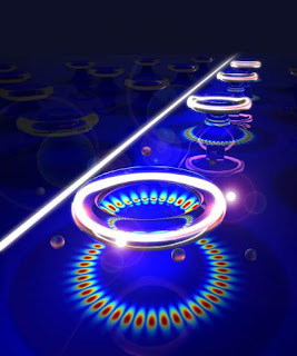
Particles About to Alight on a Whispering-Gallery Resonator

Caption: Particles that alight on the resonator disturb a light wave circulating in the torus (whose nodes and anti-nodes are visible on the torus's base) and these disturbances provide information about the particle's size. The pink line receding into the distance is an optical fiber through which light is coupled into and out of the torus.

Credit: Image by Jiangang Zhu and Jingyang Gan/WUSTL. Usage Restrictions: Please run the credit line for the image if you pick it up.

High-Q Microresonators on a Silicon Wafer

Caption: The high-Q microresonators could be mass produced by the hundreds of thousands on silicon wafers. Each torus is 20 to 30 micrometers across, one-tenth the size of the period at the end of this sentence. In this image, two particles (bright spots) have landed on the closest microresonator and are acting as scattering centers that disturb the light waves in the torus. This allows them to be detected and measured.

Credit: Image by Jiangang Zhu and Jingyang Gan/WUSTL Usage Restrictions: Please credit the image if you pick it up.
As part of this effort, a team led by Lan Yang, Ph.D., assistant professor of electrical and systems engineering, has devised a sensor on a chip that can not only detect but also measure single particles. They expect the sensor will be able to measure nanoparticles smaller than 100 nanometers in diameter (about the size of a virus particle) on the fly.

The new sensor, an improved version of a sensor called a whispering-gallery microresonator, is described in the December 13 edition of Nature Photonics's advanced online publication.

Whispering galleries

The sensor belongs to a class of devices charmingly called whispering-gallery-mode resonators.

One famous whispering gallery is St. Paul's Cathedral in London. If you stand under the dome close to the wall and speak softly to the wall, someone on the opposite side of the gallery is able to hear what you say.

The reason is the sound bounces along the wall of the gallery with very little loss of energy and so can be heard at a great distance.

However, if you speak at normal volume, what you say can no longer be understood. The sound travels around the dome more than once, and the recirculating signal gets mixed up and garbled.

Whispering-gallery microresonators

In a miniature version of a whispering gallery, laser light is coupled into a circular "waveguide," such as a glass ring. When the light strikes the boundary of the ring at a grazing angle it is reflected back into the ring.

The light wave can make many trips around the ring before it is absorbed, but only frequencies of light that fit perfectly into the circumference of the ring can do so. If the circumference is a whole number of wavelengths, the light waves superimpose perfectly each trip around.

This perfect match between the frequency and the circumference is called a resonance, or whispering-gallery mode.

The glass resonator can serve as a particle detector because the faint outer edge of the light wave, called its "evanescent tail, " penetrates the ring's surface, probing the surroundings. So when a particle attaches to the ring, it disturbs the light wave, changing the resonant frequency.
This change can be used to measure the size of the particle.

There are two problems with these microresonators, says Yang. One is that they are finicky. Lots of things can shift the resonant frequency, including vibration or temperature changes.

The other is that the frequency shift depends on where the particle lands on the ring. A particle that happens to land on a node (the dark blue areas reflected on the base of the pedestal in the accompanying image) will disturb the light wave less and appear smaller than a particle of the same size that happens to land on an anti-node (the red spots visible on the base).

For this reason the frequency shift is not a reliable measure of particle size.

The ultra-high-Q microresonator

The way around these problems is a self-referring sensing scheme possible only in an exceptionally good resonator, one with virtually no optical flaws.

Yang's lab uses surface tension to achieve the necessary perfection. The microresonators are etched out of glass layers on silicon wafers by techniques borrowed from the integrated circuit industry. These techniques allow the rings to be mass produced but leave them with rough surfaces.

In a crucial finishing step, the microresonators are reheated with a pulsed laser until the glass reflows. Surface tension then pulls the rings into smooth toruses.

"Nature helps us create the perfect structure," says Yang.

"This quality factor gives the sensor a resonance as beautiful as the pure tone form the finest musical instrument," says Jiangang Zhu, a graduate student in Yang's lab.

The Q value, or quality factor, of the reflowed resonators, a measure of microscopic imperfections that sap energy from the resonating mode, is about 100 million, meaning that light circles the ring many time. Because recirculation dramatically increases the interaction of the light wave and particles on the ring's surface, a different approach to particle detection is possible: mode splitting.

Each whispering-gallery mode is actually two modes: the light travels both clockwise and counterclockwise around the resonator. These modes are usually "degenerate," meaning they have the same frequency.

When a particle lands on a resonator, it acts as a scattering center that couples energy between the modes. The two modes re-arrange themselves so that the particle lies on a node of one and an anti-node of the other. As a result, one wave is much more perturbed than the other, and this "lifts the degeneracy," or "splits the mode."

In a low-Q resonator, the split mode can't be resolved. But in the high-Q resonator it is easily seen.

A sensor that relies on mode splitting is much less finicky than a frequency-shifting sensor. Because the clockwise and counterclockwise light waves share the same resonator, they share the same noise. Any jitter or jiggle that biases one biases the other by the same amount. Because it is self-referring, the sensor is more accurate and reliable.

Mode splitting also solves the particle location problem. The light scattering that perturbs the mode also broadens it. The mode split still varies with the location of the particle, but the ratio of the mode split and the difference between the linewidths (the breadth) of the two modes depends only on the particle's size.

To test the sensor, Daren Chen, Ph.D., associate professor of energy, environmental and chemical engineering, helped the team generate nanoparticles within specifc size ranges. In experiments with nanoparticles of salt or nanospheres of plastic, the resonator's size estimates were within one or two percent of the actual values.

"Size is a key parameter that significantly affects the physical and chemical properties of nanoparticles," says Yang. "It plays a crucial role in the applications of nanoparticles both in science and in industry, all of which will benefit from the ability to measure these particles accurately." ###

This work is partially supported by the McDonnell Academy Global Energy and Environment Partnership and the Center for Materials Innovation at Washington University.

Jiangang Zhu, Sahin Kaya Ozdemir, Yun-Feng Xioa, Lin Li, Lina He, Da-Ren Chen and Lan Yang, "On-chip Single Nanoparticle Detection and Sizing by Mode splitting in an Ultra-high-Q Microresonator, Nature Photonics, advanced online edition, Dec. 13, 2009.

Contact: Diana Lutz dlutz@wustl.edu 314-935-5272 Washington University in St. Louis

Bioactive glass nanofibers produced

A team of researchers from the University of Vigo, Rutgers University in the United States and Imperial College London, in the United Kingdom, has developed "laser spinning", a novel method of producing glass nanofibres with materials. They have been able to manufacture bioglass nanofibres, the bioactive glass used in regenerating bone, for the first time.

"Laser spinning makes it possible to produce glass nanofibres of compositions that would be impossible to obtain using other methods", Félix Quintero, co-author of the study and a researcher at the University of Vigo, tells SINC.

The new technique, which was highlighted on the front cover of the journal Advanced Functional Material, involves using a high-energy laser that melts a small amount of precursor material. This creates a super-fine filament that is lengthened and cooled by a powerful gas current.

Nanofibers of Glass Fiber

Caption: The nanofibers (and micro) of glass fiber laser produced are used for bone tissue regeneration.

Credit: Quintero et al. Usage Restrictions: None.
The scientist highlights the simplicity of the system, that "can be used in environmental conditions", as well as its high rate of production and its ability to easily control the composition of the material.

This international team has managed to produce bioglass composition nanofibres, a bioactive glass that is used to regenerate bony tissue. The laser spinning makes the material flexible, continuous and gives it a nanometric structure, which helps in the proliferation and spread of bone cells.
The researchers are now working to produce other functional compositions perfected by biomedical techniques to regenerate bone, and which may have applications in other fields. The technique could be used to manufacture fire-retardant fabrics, CO2 capture systems, or to produce composite materials that require reinforcement with nanofibres. ###

Aside from the scientists from the University of Vigo, a research group from Rutgers University in the United States and another from Imperial College London, in the United Kingdom, also took part in this initiative.

References:

Félix Quintero, Juan Pou, Rafael Comesaña, Fernando Lusquiños, Antonio Riveiro, Adrian B. Mann, Robert G. Hill, Zoe Y. Wu y Julian R. Jones. "Laser Spinning of Bioactive Glass Nanofibers". Advanced Functional Material 19 (19): 3084, 2009.

Contact: SINC info@plataformasinc.es 34-914-251-820 FECYT - Spanish Foundation for Science and Technology

Wednesday, January 27, 2010

Within a cell, actin keeps things moving

University of Oregon-made technique is putting new light on machinery driving intracellular transport.

Using new technology developed in his University of Oregon lab, chemist Andrew H. Marcus and his doctoral student Eric N. Senning have captured what they describe as well-orchestrated, actin-driven, mitochondrial movement within a single cell.

That movement -- documented in a paper appearing online the week of Dec. 14-18 ahead of regular publication in the Proceedings of the National Academy of Sciences -- appears to be coordinated by mitochondria's recruitment of actin-related proteins that rapidly assemble into extended fractal-like structures in a molecular chemical reaction known as polymerization.

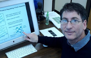
Andrew H. Marcus, University of Oregon

Caption: UO chemist Andrew Marcus has found that actin recruited by mitochondrial cells drive transport in budding yeast cells.

Credit: University of Oregon. Usage Restrictions: None.
The coordinated movement of mitochondria is important for reproduction of identical daughter cells, and the sorting of mitochondrial DNA into the spinoff cells.

The research was done with a molecular fluorescence technology called Fourier imaging correlation spectroscopy that allows researchers using focused laser beams to see, measure and map the intermittent movement of mitochondria at micron scales. Marcus will discuss the technology,
developed with funding from the National Institutes of Health and National Science Foundation, at the 2010 annual meeting of the American Physical Society in Portland, Ore., in March. It also was detailed in a paper published online in October by the journal Annual Reviews of Physical Chemistry.

In their project published by PNAS -- funded by the NIH -- Senning and Marcus looked at actin's behavior using inhibitory agents to monitor mitochondrial activity in Saccharomyces cerevisiae, a species of budding yeast often used in research. They also introduced two defective forms of the protein. Their technique included the use of hormones to trick a yeast cell into thinking it was about to mate, so that it stops dividing and sits and fluctuates -- much like a car in idle. From this state, the images are drawn.

The picture that emerged, Marcus said, was that actin is drawn to the surfaces of mitochondria to regulate the polymerization machinery so that it operates in an efficient, organized manner. The findings, the researchers wrote, lend support to an existing model in which non-equilibrium forces are directly coupled to mitochondrial membrane surfaces. In effect, the findings support the idea that despite the cramped quarters of molecules in densely packed cells, intracellular transport is accomplished by coordinating the movements of a multi-faceted machine, rather than resulting from random (Brownian) movements of material based on what obstacles will allow.

The quest for understanding the machinery is more than just biological, where this research provides insight into how the cell moves its mitochondria into the daughter cells, Marcus said. The knowledge could become useful in the production of nanotechnology devices.

"A central question in modeling cell transport is whether the cytoplasm may be viewed as a simple extension of a complex fluid at equilibrium or if non-equilibrium effects dominate the motions of intracellular species," he said. "If somebody wants to design a micron-scale machine or make a self-replicating device, one would have to have these physical principles in place. One would need to have a motor in place and know how much force the motor needs to apply, either cooperatively or individually with other components." ###

Marcus is a member of the UO's Oregon Center for Optics, and an associate member of the Institute of Molecular Biology and the Materials Science Institute.

About the University of Oregon

The University of Oregon is a world-class teaching and research institution and Oregon's flagship public university. The UO is a member of the Association of American Universities (AAU), an organization made up of the 62 leading public and private research institutions in the United States and Canada. The UO is one of only two AAU members in the Pacific Northwest.

Source: Andrew H. Marcus, associate professor of chemistry, 541-346-4809, ahmarcus@uoregon.edu

Links:Contact: Jim Barlow
jebarlow@uoregon.edu
541-346-3481 University of Oregon

Tuesday, January 26, 2010

Water Droplets Shape Graphene Nanostructures

Graphene -- a single-atom-thick sheet of carbon, like those seen in pencil marks -- offers great potential for new types of nanoscale devices, if a good way can be found to mold the material into desired shapes.

Chemists at the University of Illinois at Chicago say it's possible, reporting that graphene can become quite pliable using only a nanodroplet of water to do the job.

"Up until now, it wasn't thought we could controllably fold these structures," said Petr Král, assistant professor of chemistry at UIC. "But now we know how to shape graphene by using weak forces between nanodroplets carefully positioned on graphene sheets."

Petr Král

Petr Král
Král and two of his graduate students described the process in a recent article in Nano Letters, which is highlighted in Nature's "news and views" section Dec. 17.

Engineers already cut graphene into narrow ribbons and other shapes, expanding the set of carboneous systems such as fullerenes, carbon nanotubes and nano-diamonds. Using computer simulations, Král showed that weak molecular interactions called van der Waals forces between water nanodroplets and graphene can shape it into a wide variety of forms,
without the water and graphene chemically binding.

"Depending on the size of the water droplet and the shape and size of graphene flake used, we can fold it in different shapes for various applications," said Král. "It's similar to the way proteins are folded in biological cells with the help of chaperone proteins."

Král and his students discovered they could use water droplets to roll, bend, slide and shape graphene into different complex structures such as capsules, sandwiches, knots and rings –- all potential building blocks of nanodevices with unique mechanical, electrical or optical properties. By using special techniques like atomic force microscopy and carefully guided microscopic needles, water droplets and other materials can be carefully positioned on graphene to shape it into desired forms, he says.

Král's laboratory is studying potential uses of nanoscale graphene, such as ways to coat it with phospholipid molecules that would allow it to become part of biological cell membranes where it might perform specific functions. His lab is also designing graphene sheet nanoscale pores that allow the building of novel ion and molecular separation membranes for use in desalination and other applications.

While the materials he works with are inorganic, Král sees a growing trend to developing hybrid multifunctional systems that combine inorganic nanostructures with biological cellular systems.

"We're trying to detect signals from the biological world or pass signals to the biological world," he said. "In the future, perhaps proteins will evolve to interact with inorganic systems. It's a way of evolution to form a new interface, or hybrid system, working together on novel functions."

The Nano Letters article was co-authored by Niladri Patra, a UIC chemistry doctoral student and first author on the paper, and former UIC doctoral student Boyang Wang, now a post-doctoral fellow at Northwestern University.

Král's research is supported by the National Science Foundation.

Contact: Paul Francuch francuch@uic.edu 312-996-3457 University of Illinois at Chicago

Monday, January 25, 2010

Researchers find cells move in mysterious ways VIDEO

PROVIDENCE, R.I. [Brown University] — Our cells are more like us than we may think. They're sensitive to their environment, poking and prodding deliberately at their surroundings with hand-like feelers and chemical signals as they decide whether and where to move. Such caution serves us well but has vexed engineers who seek to create synthetic tissue, heart valves, implants and other devices that the human body will accept.

To overcome that obstacle, scientists have sought to learn more about how cells explore what's around them. While numerous studies have looked at cellular movement in two dimensions and a few recent experiments involved cellular motion in three dimensions, scientists remained unsure just how much cells interacted with their surroundings.


Caption: Scientists at Brown University and the California Institute of Technology have for the first time tracked how cells move in three dimensions by measuring the force exerted by them on their surroundings. The video shows how cells engage in "pushing and pulling" as they probe their surroundings and move.

Credit: Christian Franck, Brown University. Usage Restrictions: None.

3-D Cell

Caption: Scientists at Brown University and the California Institute of Technology have for the first time tracked how cells move by measuring the force exerted by them on their surroundings. The method could lead to better understanding how healthy cells differ from malignant cells.

Credit: Christian Franck, Brown University. Usage Restrictions: None.
Now, a study involving Brown University and the California Institute of Technology has recorded for the first time how cells move in three dimensions by measuring the force exerted by cells on their environs. The research gives scientists their most complete assessment to date about how cells move.

"We've learned that cells move in much more complex ways than previously believed," said Christian Franck, assistant professor in engineering at Brown and the co-lead author of the study published online in the Proceedings of the National Academy of Sciences. "Now, we can start to really put numbers on how much cells push and pull on their environment and how much cells stick to tissues as they move around and interact."

In the study, Franck and co-lead author Stacey Maskarinec, who both conducted the experiments while graduate students at the California Institute of Technology, placed cells on top of a 50-micron-thick water-based gel designed to mimic human tissue. They added into the gel spheres about a half-micron in diameter that lit up when jostled by the cells' actions. By combining two techniques — laser scanning confocal microscopy and digital volume correlation — the scientists tracked the cells' movement by quantifying exactly how the environment changed each time the cell moved. The team recorded results every 35 minutes over a 24-hour period.
What they found was cells move in intriguing ways. In one experiment, a cell is clearly shown operating in three dimensions by extending feelers into the gel, probing at depth, as if thrusting a leg downward in a pool. The Brown and Caltech scientists also found that as a cell moves, it engages in a host of push-pull actions: It redistributes its weight, it coils and elongates its body, and it varies the force with which it "grips," or adheres, to a surface. Combined, the actions help the cell generate momentum and create a "rolling motion," as Franck described it, that is more like walking than shuffling, as many scientists had previously characterized the movement.

"The motion itself is in three dimensions," Franck said.

Franck's lab plans to use the new force-measurement technique to examine how the movement of normal healthy cells differs from mutant or malignant ones. "That promises to give us greater insight in how cells' behavior changes when they become diseased," Franck said. ###

David Tirrell and Guruswami Ravichandran, scientists at Caltech, contributed to the research. The National Science Foundation funded the work.

Contact: Richard Lewis Richard_Lewis@Brown.edu 401-863-3766 Brown University

Saturday, January 23, 2010

Nanoemulsion treatment advances with GSK agreement

Nanoemulsion anti-infection agents reach milestone.

ANN ARBOR, Mich. — GlaxoSmithKline and Ann Arbor-based NanoBio Corporation announced today that they have signed an exclusive over-the-counter licensing agreement for NanoBio's unique nanoemulsion treatment for cold sores in the United States and Canada.

James R. Baker, Jr., M.D., director of the Michigan Nanotechnology Institute for Medicine and Biological Sciences at the University of Michigan Medical School, developed nanoemulsions in the 1990s at U-M and founded NanoBio Corporation to further develop and commercialize the technology.

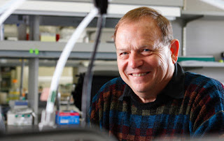
Dr. James R. Baker, Jr., University of Michigan Health System

Caption: Dr. James R. Baker developed nanoemulsions in the 1990s. He is director of the Michigan Nanotechnology Institute for Medicine and Biological Sciences at the University of Michigan.

Credit: University of Michigan. Usage Restrictions: None.
The nanoemulsion technology is patented by U-M and licensed to NanoBio Corporation. Dr. Baker serves as CEO of NanoBio Corporation, where he holds a financial interest. At U-M, he also is the Ruth Dow Doan Professor of Internal Medicine and allergy division chief.

"For the university, this agreement between NanoBio and GlaxoSmithKline demonstrates the value of our technology and fulfills our goal of getting the benefits of our research deployed broadly to the general public," says Ken Nisbet, executive director of the U-M Office of Technology Transfer.

"We're very proud of the accomplishments of Dr. Baker and the entire NanoBio team."

Under the new agreement, New Jersey-based GlaxoSmithKline will pay NanoBio an up-front fee of $14.5 million for licensing rights for the nanoemulsion product called NB-001.
NanoBio is eligible to receive additional milestone payments of up to $40 million plus high single-digit royalties on future sales.

Nanoemulsions are superfine mixtures of soybean oil and water, stabilized by surfactants and blended at very high speeds so that the resulting droplets are less than 400 nanometers in diameter. Nanoemulsion droplets fuse with a microbe's outer membrane, disrupt the membrane and kill the organism.

Baker believes that the GlaxoSmithKline-NanoBio partnership will "enable the development and commercialization of NB-001 to its fullest potential and validates the promise of our proprietary platform technology, and its potential use in a wide range of dermatological and anti-infective applications."

NB-001 is the first nanoemulsion therapeutic to complete successful phase 2 clinical trials and will enter phase 3 testing within the next six months. NanoBio is developing other nanoemulsion-based therapies for a range of diseases including fungal infections, acne and molluscum contagiosum. ###

Cold sores, caused by Herpes labialis an infection caused by the herpes simplex virus, affect about one-fifth of adults in the United States. NB001 will add to GSK's Abreva line of over-the-counter medications for cold sores.

References: More about the Michigan Nanotechnology Institute nano.med.umich.edu

More about nanoemulsions nano.med.umich.edu/Platforms/Antimicrobial-Nanoemulsion

More about the U-M Office of Technology Transfer www.techtransfer.umich.edu/

Contact: Anne Rueter arueter@umich.edu 734-764-2220 University of Michigan Health System

Friday, January 22, 2010

Thermochemical nanolithography now allows multiple chemicals on a chip

Allows controlled attachment of nano-objects to be performed weeks apart in any lab.

Scientists at Georgia Tech have developed a nanolithographic technique that can produce high-resolution patterns of at least three different chemicals on a single chip at writing speeds of up to one millimeter per second. The chemical nanopatterns can be tailor-designed with any desired shape and have been shown to be sufficiently stable so that they can be stored for weeks and then used elsewhere. The technique, known as Thermochemical Nanolithography is detailed in the December 2009 edition of the journal Advanced Functional Materials. The research has applications in a number of scientific fields from electronics to medicine.

Thermochemical Nanolithography

Caption: Scientists at Georgia Tech have developed a nanolithographic technique that can produce high-resolution patterns of at least three different chemicals on a single chip at writing speeds of up to one millimeter per second. The chemical nanopatterns can be tailor-designed with any desired shape and have been shown to be sufficiently stable so that they can be stored for weeks and then used elsewhere.

Credit: Eric Huffman/Georgia Tech. Usage Restrictions: With Credit.
"The strength of this method is really the possibility to produce low-cost, high-resolution and high-density chemical patterns on a sample that can be delivered in any lab around the world, where even non experts in nanotechnology can dip the sample in the desired solution and, for example, make nano-arrays of proteins, DNA or nanoparticles," said Elisa Riedo, associate professor in the School of Physics at the Georgia Institute of Technology.

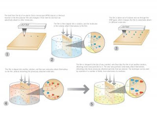
Conceptually, the technique is surprisingly simple. Using an atomic force microscope (AFM), researchers heat a silicon tip and run it over a thin polymer film. The heat from the tip induces a local chemical reaction at the surface of the film.
This reaction changes the film's chemical reactivity and transforms it from an inert surface to a reactive one that can selectively attach other molecules. The team first developed the technique in 2007. Now they've added some important new twists that should make thermochemical nanolithography (TCNL) an extremely useful tool for scientists working at the nanoscale.

"We've created a way to make independent patterns of multiple chemicals on a chip that can be drawn in whatever shape you want," said Jennifer Curtis, assistant professor in the School of Physics.

Being able to create high-resolution features of different chemicals in arbitrary shapes is important because some nanolithography techniques are limited to just one chemistry, lower resolutions and/or fixed shapes. In addition, TCNL's speed capability of one millimeter per second makes it orders of magnitude faster than the widely used dip-pen nanolithography, which routinely clocks at a speed of 0.0001 millimeters per second per pen.

The research is enabled by heated AFM probe tips that can create a hot spot as small as a few nanometers in diameter. Such tips are designed and fabricated by collaborator Professor William King at the University of Illinois, Urbana-Champaign. "The heated tip allows one to direct nano-scale chemical reactions," said King.

The new technique produces multiple chemical patterns on the same chip by using the AFM to heat a polymer film and change its reactivity. The chip is then dipped into a solution, which allows chemicals (for example, proteins or other chemical linkers) in the solution to bind to the chip on the parts where it has been heated. The AFM then heats the film in another spot. The chip is dipped into another solution and again another chemical can bind to the chip.

In the paper, the scientists show they can pattern amine, thiol, aldehyde and biotin using this technique. But in principle TCNL could be used for almost any chemical. Their work also shows that the chemical patterns can be used to organize functional materials at the surface, such as proteins and DNA.

"The power of this technique is that in principle it can work with almost any chemical or chemically reactive nano-object. It allows scientists to very rapidly draw many things that can then be converted to any number of different things, which themselves can bind selectively to yet any number of other things. So, it doesn't matter if you're interested in biology, electronics, medicine or chemistry, TCNL can create the reactive pattern to bind what you choose," said Seth Marder, professor in Tech's School of Chemistry and Biochemistry and director of the Center for Organic Photonics and Electronics.

In addition, TCNL allows the chemical writing to be done in one location with the nano-object patterning in another, so that scientists who aren't experts in writing chemical patterns on the nanoscale can still attach their objects to it. It's the technique's stability that makes this possible.

"Once you draw the pattern, it's very stable and non-reactive. We've shown that you can have it for more than a month, take it out and dip it and it still will bind," said Riedo.

"I would like to think that several years from now people will have access to a TCNL tool that enables them to do this patterning at a place like Georgia Tech, that's much less expensive than the kind of nanolithography tools we currently use in our clean room," said Marder. ###

The research was supported by the National Science Foundation, the U.S. Department of Energy, the Georgia Institute of Technology, GT Innovative Award, and ONR Nanoelectronics.

Contact: David Terraso david.terraso@comm.gatech.edu 404-385-2966 Georgia Institute of Technology

Thursday, January 21, 2010

Researchers take the inside route to halt bleeding

Synthetic platelets halve clotting time

Blood loss is a major cause of death from roadside bombs to freeway crashes. Traumatic injury, the leading cause of death for people age 4 to 44, often overwhelms the body's natural blood-clotting process.

In an effort to enhance the natural process, a team led by Erin Lavik, a new Case Western Reserve University biomedical engineering professor, and her former doctoral student, James P. Bertram, built synthetic platelets that show promise in halting internal and external bleeding.

Their work is published in Science Translational Medicine.

Erin Lavik

Erin Lavik
The researchers were inspired by studies showing there are few options to treat soldiers suffering from internal injuries in Afghanistan and Iraq. They wanted to develop a treatment medics can keep in their field packs.

"The military has been phenomenal at developing technology to halt bleeding, but the technology has been effective only on external or compressible injuries," Lavik said. "This could be a compliment to current therapies."
Blood platelets are the structural and chemical foundation of blood clotting, a complex cascade of events that works well with normal cuts and scrapes but can be overmatched by serious injury.

Using other's platelets can enhance clotting but carries risks of several complications. And these platelets must be refrigerated and have a short shelf life.

Bertram and Lavik developed platelets made from biodegradable polymers. The synthetic platelets are designed to home in and link up with natural platelets at the site of an injury.

In essence, adding artificial platelets to a traumatic injury site is akin to adding sand bags to a levy along a flooding river.

The natural platelets, activated by injury, emit chemicals that bind natural platelets and the additional synthetics into a larger clot that quickly stems the bleeding.

In testing, rat models injected with synthetic platelets prior to injury stopped bleeding in half the time of untreated models. Untreated models injected 20 seconds after injury stopped bleeding in 23 percent less time than models left untreated.

In another comparison, the artificial platelets resulted in clotting times about 25 percent faster than wounds treated with recombinant factor VIIa, which is the current state of the art treatment for uncontrolled bleeding in surgery and emergency rooms. While the recombinant factor is used on various injuries, its cost can be in the tens of thousands of dollars per treatment and is not used in patients suffering head or spinal cord injuries, due to risk of complications.

Lavik said her team made platelets from polymers already used in treatments approved by the Food and Drug Administration in hopes the new treatment might be approved faster. They also built the parts of the synthetic platelets that bind to natural platelets from relatively short pieces of proteins because they're more stable than longer pieces and cheaper.

To avoid formation of an artificial clot, each synthetic platelet is built with a surrounding water shield. Fluorescing compounds showed the synthetic platelets not bound in clots were flushed from the rat model's system in a day. No ill effects were seen in the following week.

Testing also showed the synthetic platelets remain viable after sitting on a shelf for at least two weeks.

Lavik is seeking grants to further test the platelets. ###

Case Western Reserve University is among the nation's leading research institutions. Founded in 1826 and shaped by the unique merger of the Case Institute of Technology and Western Reserve University, Case Western Reserve is distinguished by its strengths in education, research, service, and experiential learning. Located in Cleveland, Case Western Reserve offers nationally recognized programs in the Arts and Sciences, Dental Medicine, Engineering, Law, Management, Medicine, Nursing, and Social Work. www.case.edu.

Contact: Kevin Mayhood kevin.mayhood@case.edu 216-368-4442 Case Western Reserve University

Wednesday, January 20, 2010

New bacterial behavior observed

PNAS study documents puzzling movement of electricity-producing bacteria near energy sources

Bacteria dance the electric slide, officially named electrokinesis, in a new study by USC geobiologists.

The study, published online in the Proceedings of the National Academy of Sciences Early Edition, describes a bacterial behavior never before observed.

The metal-metabolizing Shewanella oneidensis microbe does not just cling to metal in its environment, as previously thought. Instead, it harvests electrochemical energy obtained upon contact with the metal and swims furiously for a few minutes before landing again.

Kenneth Nealson

Study co-author Kenneth Nealson. Photo credit Philip Channing.
Electrokinesis is more than a curiosity. Laboratory director and co-author Kenneth Nealson, the Wrigley Professor of Geobiology at USC College and discoverer of Shewanella, hopes to boost the power of microbe-based fuel cells enough to produce usable energy.

The discovery of electrokinesis does not achieve that goal directly, but it should help researchers to better tune the complex living engines of microbial fuel cells.
“To optimize the bacteria is far more complicated than to optimize the fuel cell,” Nealson said.

Electrokinesis was discovered in 2007 by Nealson’s graduate student Howard Harris, an undergraduate at the time.

Nealson had given Harris what seemed an ideal assignment for a double major in cinema and biophysics.

“I had asked him if he would just take some movies of these bacteria doing what they do,” Nealson said.

Filming through a microscope is hardly simple, but with the help of co-author and biophysics expert Moh El-Naggar, assistant professor of physics and astronomy at USC College, Harris was able to make a computer analysis of a time-lapse sequence of bacteria near metal oxide particles.

“Every time the bacteria were around these particles … there was a great deal of swimming activity,” Nealson recalled.

Harris then discovered that bacteria displayed the same behavior around the electrode of a battery. The swimming stopped when the electrode turned off, suggesting that the activity was electrical in origin.

As is often true with discoveries, this one raises more questions than it answers. Two in particular intrigue the researchers:

* Why do the bacteria expend valuable energy swimming around?
* How do the bacteria find the metal and return to it? Do they sense it through an electric field or the behavior of other bacteria?

Nealson and his team so far have only educated guesses.

For the first question, Nealson believes that the bacteria may swim away from the metal because they have too many competitors.

Bacteria get energy in two steps: by absorbing dissolved nutrients and then by converting those nutrients into biologically useful forms of energy through respiration, or the loss of electrons to an electron acceptor such as iron or manganese (humans also respire through the loss of electrons to oxygen, one of the most powerful electron acceptors).

“If electrons don’t flow, it doesn’t matter how much food you have,” Nealson said.

However, he added, “in some environments, the food is much more precious than the electron acceptors.”

If a metal surface became too crowded for bacteria to absorb nutrients easily, they might want to swim away and come back.

For the second question, Harris and co-author Mandy Ward, assistant professor of research in earth sciences at USC College, are planning other experiments to understand exactly how Shewanella find electron acceptors.

They expect the experiments to keep Harris busy through his doctoral thesis.

The other co-authors on the paper were Orianna Bretschger of the J. Craig Venter Institute in San Diego, Margaret Romine of the Pacific Northwest National Laboratory and Anna Obraztsova, a staff scientist in the Nealson laboratory at USC.

Contact: Carl Marziali marziali@usc.edu 213-740-4751 University of Southern California

Monday, January 18, 2010

University of Toronto physicists lay the groundwork for cooler, faster computing

University of Toronto quantum optics researchers Sajeev John and Xun Ma have discovered new behaviours of light within photonic crystals that could lead to faster optical information processing and compact computers that don’t overheat.

“We discovered that by sculpting a unique artificial vacuum inside a photonic crystal, we can completely control the electronic state of artificial atoms within the vacuum,” says Ma, a PhD student under John’s supervision and lead author of a study published in a recent issue of Physical Review Letters. “This discovery can enable photonic computers that are more than a hundred times faster than their electronic counterparts, without heat dissipation issues and other bottlenecks currently faced by electronic computing.”

Sajeev John

Sajeev John
“We designed a vacuum in which light passes through circuit paths that are one one-hundredth of the thickness of a human hair, and whose character changes drastically and abruptly with the wavelength of the light,” says John. “A vacuum experienced by light is not completely empty, and can be made even emptier. It’s not the traditional understanding of a vacuum.”
“In this vacuum, the state of each atom – or quantum dot – can be manipulated with color-coded streams of laser pulses that sequentially excite and de-excite it in trillionths of a second. These quantum dots can in turn control other streams of optical pulses, enabling optical information processing and computing,” says Ma.

The original aim of the investigation was to gain a deeper understanding of optical switching, part of an effort to develop an all-optical micro-transistor that could operate within a photonic chip. This led to the discovery of a new and unexpected dynamic switching mechanism, imposed by the artificial vacuum in a photonic crystal. The research also led to the discovery of corrections to one of the most fundamental equations of quantum optics known as the Bloch equation.

“This new mechanism enables micrometer scale integrated all-optical transistors to perform logic operations over multiple frequency channels in trillionths of a second at microwatt power levels, which are about one millionth of the power required by a household light bulb,” says John. “That this mechanism allows for computing over many wavelengths as opposed to electronic circuits which use only one channel, would significantly surpass the performance of current day electronic transistors.”

The results appear in a paper titled “ Ultrafast Population Switching of Quantum Dots in a Structured Vacuum”, published online in the Physical Review Letters on December 3. The research was funded with support from the Natural Sciences and Engineering Research Council of Canada, the Canadian Institute for Advanced Research, and the Ontario Premier’s Platinum Research Fund.

Contact: Sean Bettam s.bettam@utoronto.ca 416-946-7950 University of Toronto

Sunday, January 17, 2010

Nanoprobes hit targets in tumors, could lessen chemo side effects

WEST LAFAYETTE, Ind. - Tiny nanoprobes have shown to be effective in delivering cancer drugs more directly to tumor cells - mitigating the damage to nearby healthy cells - and Purdue University research has shown that the nanoprobes are getting the drugs to right cellular compartments.

Professor Joseph Irudayaraj and graduate student Jiji Chen, both in the Department of Agricultural and Biological Engineering, have found that the nanoprobes, or nanorods, when coated with the breast cancer drug Herceptin, are reaching the endosomes of cells, mimicking the delivery of the drug on its own. Endosomes perform a sorting function to deliver drugs and other substances to the appropriate locations.

Joseph Irudayaraj

Purdue professor Joseph Irudayaraj uses a magnet to attract tiny magnetic particles in a solution. Irudayaraj designed nanoprobes with gold and magnetic particles that could be used to deliver drugs directly to cancer cells. Credit: Tom Campbell / Purdue Agricultural
"We have demonstrated the ability to track these nanoparticles in different cellular compartments of live cells and show where they collect quantitatively," said Irudayaraj, whose results were published early online in the journal ACS Nano. "Our methods will allow us to calculate the quantities of a drug needed to treat a cancer cell because now we know how these nanoparticles are being distributed to different parts of the cell."

The nanoprobes, which are about 1,000 times smaller than the diameter of a human hair, are made from gold and magnetic particles.
An MRI machine can track the magnetic portions of the nanoprobes while a more sensitive microscopy process can detect the gold.

The nanoprobes were inserted into live human tumor cells during laboratory testing. Using fluorescent markers to differentiate organelles, or sub-units of cells, Irudayaraj's group was able to determine the number of nanoprobes accumulating in the endosomes, lysosomes and membranes of those cells.

Cancer treatments often use high drug concentrations that damage healthy cells near a tumor. While Herceptin is attracted to and attaches to the proteins on the surface of breast cancer cells, healthy surrounding cells absorb some of the chemotherapy drugs through normal fluidic intake.

Irudayaraj said targeting only tumor cells with nanoprobes would require less drugs and mitigate the side effects of cancer chemotherapy drugs.

"Each nanoparticle acts like a deliverer of a mail package, or dose, of the drug directly to the appropriate location," Irudayaraj said.

In Irudayaraj's laboratory tests, endosomes received a major portion of the nanorods containing Herceptin. Lysosomes, which act like garbage collection units in cells and hinder a drug's effectiveness, received a lower concentration of nanorods.

Irudayaraj said those percentages are similar to how cells distribute drugs through traditional treatments.

Irudayaraj will next try to attach multiple drugs to a nanoparticle and track their distribution within cells. He also wants to determine the timing of a drug's release from the nanoprobes after attaching to the tumor cells. ###

The research was funded through a Trask Grant and the Purdue Research Foundation.

Contact: Brian Wallheimer bwallhei@purdue.edu 765-496-2050. Source: Joseph Irudayaraj, 765-494-0388 josephi@purdue.edu WEB: Purdue University

ABSTRACT

Quantitative Investigation of Compartmentalized Dynamics of ErbB2 Targeting Gold Nanorods in Live Cells by Single Molecule Spectroscopy

Jiji Chen and Joseph Irudayaraj

Understanding the diffusion dynamics and receptor uptake mechanism of nanoparticles in cancer cells is crucial to the rational design of multifunctional nanoprobes for targeting and delivery. In this report, for the first time, we quantify the localization and evaluate the diffusion times of Herceptin-conjugated gold nanorods (H-GNRs) in different cell organelles by fluorescence correlation spectroscopy (FCS) and examine the endocytic diffusion of H-GNRs in live ErbB2 overexpressing SK-BR-3 cells. First, by colocalizing H-GNRs in different cellular organelles depicted by the respective markers, we demonstrate that H-GNRs colocalize with the endosome and lysosome but not with the Golgi apparatus.

Our study shows that Herceptin-conjugated GNRs have similar intracellular localization characteristics as Herceptin−ErbB2 complex, with a higher concentration found in the endosome (72 ± 20.6 nM) than lysosome (9.4 ± 4.2 nM) after internalization. The demonstrated approach and findings not only lay the foundations for a quantitative understanding of the fate of nanoparticle-based targeting but also provide new insights into the rational design of nanoparticle delivery systems for effective treatment.

Saturday, January 16, 2010

Tracking new cancer-killing particles with MRI

Nanoparticle could allow diagnosis, treatment in one visit.

HOUSTON -- (Dec. 14, 2009) -- Researchers at Rice University and Baylor College of Medicine (BCM) have created a single nanoparticle that can be tracked in real time with MRI as it homes in on cancer cells, tags them with a fluorescent dye and kills them with heat. The all-in-one particle is one of the first examples from a growing field called "theranostics" that develops technologies physicians can use to diagnose and treat diseases in a single procedure.

The research is available online in the journal Advanced Functional Materials. Tests so far involve laboratory cell cultures, but the researchers said MRI tracking will be particularly advantageous as they move toward tests in animals and people.


Caption: This is Naomi Halas from Rice University. Credit: Rice University. Usage Restrictions: Must credit.
"Some of the most essential questions in nanomedicine today are about biodistribution -- where particles go inside the body and how they get there," said study co-author Naomi Halas. "Noninvasive tests for biodistribution will be enormously useful on the path to FDA approval, and this technique -- adding MRI functionality to the particle you're testing and using for therapy -- is a very promising way of doing this."

Halas, Rice's Stanley C. Moore Professor in Electrical and Computer Engineering and professor of chemistry and biomedical engineering, is a pioneer in nanomedicine. The all-in-one particles are based on nanoshells -- particles she invented in the 1990s that are currently in human clinical trials for cancer treatment.
Nanoshells harvest laser light that would normally pass harmlessly through the body and convert it into tumor-killing heat.

In designing the new particle, Halas partnered with Amit Joshi, assistant professor in BCM's Division of Molecular Imaging, to modify nanoshells by adding a fluorescent dye that glows when struck by near-infrared (NIR) light. NIR light is invisible and harmless, so NIR imaging could provide doctors with a means of diagnosing diseases without surgery.

In studying ways to attach the dye, Halas' graduate student, Rizia Bardhan, found that dye molecules emitted 40-50 times more light if a tiny gap was left between them and the surface of the nanoshell. The gap was just a few nanometers wide, but rather than waste the space, Bardhan inserted a layer of iron oxide that would be detectable with MRI. The researchers also attached an antibody that lets the particles bind to the surface of breast and ovarian cancer cells.

In the lab, the team tracked the fluorescent particles and confirmed that they targeted cancer cells and destroyed them with heat. Joshi said the next step will be to destroy whole tumors in live animals. He estimates that testing in humans is at least two years away, but the ultimate goal is a system where a patient gets a shot containing nanoparticles with antibodies that are tailored for the patient's cancer. Using NIR imaging, MRI or a combination of the two, doctors would observe the particles' progress through the body, identify areas where tumors exist and then kill them with heat.

"This particle provides four options -- two for imaging and two for therapy," Joshi said. "We envision this as a platform technology that will present practitioners with a choice of options for directed treatment."

Eventually, Joshi said, he hopes to develop specific versions of the particles that can attack cancer at different stages, particularly early stage cancer, which is difficult to diagnose and treat with current technology. The researchers also expect to use different antibody labels to target specific forms of the disease. Halas said the team has been careful to choose components that are either already approved for medical use or are already in clinical trials.

"What's nice is that every single component of this has been approved or is on a path toward FDA approval," Halas said. "We're putting together components that all have good, proven track records." ###

Bardhan and BCM postdoctoral researcher Wenxue Chen are co-primary authors of the paper. Additional Rice co-authors include Emilia Morosan, assistant professor of physics and astronomy, and graduate students Ryan Huschka and Liang Zhao. Additional BCM co-authors include Robia Pautler, assistant professor of neuroscience and radiology, postdoctoral researcher Marc Bartels and graduate student Carlos Perez-Torres.

The research was sponsored by the Air Force Office of Scientific Research, the Welch Foundation and the Department of Defense's Multidisciplinary University Research Initiative.

View the paper at tinyurl.com/nanocomplex. Contact: Jade Boyd jadeboyd@rice.edu 713-348-6778 Rice University

Friday, January 15, 2010

Scientists use nanosensors for first time to measure cancer biomarkers in blood

New Haven, Conn.—A team led by Yale University researchers has used nanosensors to measure cancer biomarkers in whole blood for the first time. Their findings, which appear December 13 in the advanced online publication of Nature Nanotechnology, could dramatically simplify the way physicians test for biomarkers of cancer and other diseases.

The team—led by Mark Reed, Yale's Harold Hodgkinson Professor of Engineering & Applied Science, and Tarek Fahmy, an associate professor of biomedical and chemical engineering—used nanowire sensors to detect and measure concentrations of two specific biomarkers: one for prostate cancer and the other for breast cancer.

Nanosensor

Caption: Blood is filtered and transferred to nanosensors on a chip, which can detect and measure cancer biomarkers.

Credit: Mark Reed/Yale University. Usage Restrictions: Image may be used with appropriate credit.
"Nanosensors have been around for the past decade, but they only worked in controlled, laboratory settings," Reed said. "This is the first time we've been able to use them with whole blood, which is a complicated solution containing proteins and ions and other things that affect detection."

To overcome the challenge of whole blood detection, the researchers developed a novel device that acts as a filter, catching the biomarkers—in this case, antigens specific to prostate and breast cancer—on a chip while washing away the rest of the blood.
Creating a buildup of the antigens on the chip allows for detection down to extremely small concentrations, on the order of picograms per milliliter, to within an accuracy of plus or minus 10 percent. This is the equivalent of being able to detect the concentration of a single grain of salt dissolved in a large swimming pool.

Until now, detection methods have only been able to determine whether or not a certain biomarker is present in the blood at sufficiently high concentrations for the detection equipment to give reliable estimates of its presence. "This new method is much more precise in reading out concentrations, and is much less dependent on the individual operator's interpretation," Fahmy said.

In addition to relying on somewhat subjective interpretations, current tests are also labor intensive. They involve taking a blood sample, sending it to a lab, using a centrifuge to separate the different components, isolating the plasma and putting it through an hours-long chemical analysis. The whole process takes several days. In comparison, the new device is able to read out biomarker concentrations in a just a few minutes.

"Doctors could have these small, portable devices in their offices and get nearly instant readings," Fahmy said. "They could also carry them into the field and test patients on site."

The new device could also be used to test for a wide range of biomarkers at the same time, from ovarian cancer to cardiovascular disease, Reed said. "The advantage of this technology is that it takes the same effort to make a million devices as it does to make just one. We've brought the power of modern microelectronics to cancer detection." ###

Authors of the paper include Eric Stern, Aleksandar Vacic, Nitin Rajan, Jason Criscione, Jason Park, Mark Reed and Tarek Fahmy (all of Yale University); Bojan Ilic (Cornell University); David Mooney (Harvard University).

Citation: 10.1038/NNANO.2009.353

Contact: Suzanne Taylor Muzzin suzanne.taylormuzzin@yale.edu 203-432-8555 Yale University

Thursday, January 14, 2010

New curriculum mixes nanotechnology and skiing VIDEO

$200,000 National Science Foundation grant for University of Nevada, Reno. nanotechnology and skiing VIDEO, MPEG4 30 mb

RENO, Nev. – Nanotechnology seems a daunting subject, but for mechanical engineering students at the University of Nevada, Reno, it has taken on a real world approach – in Ski Building 101.

"Yes, we're going to make skis. No, it's not really Ski Building 101," said Kam K. Leang, the faculty member and principal investigator for a project to further integrate nanotechnology into the undergraduate curriculum at the University.

Leang and two colleagues at the University, Jonghwan Suhr and John Cannon, aim to prepare 21st century mechanical engineers at the University to meet the emerging challenges of nanotechnology using a top-down approach where the first important step is to excite them about the technology.

nanotechnology and skiing

Caption: Students in a mechanical engineering design class at the University of Nevada, Reno remove from the ski press a new ski with a novel vibration dampening design.

Credit: Photo by Mike Wolterbeek, University of Nevada, Reno. Usage Restrictions: None.
"We want students to get enthused about mechanical engineering, to see the possibilities and potential of nanotechnology," Leang said.

Leang, who's been building skis for more than five years in his garage and offers web-based instructions on ski building, has plans for the students to use innovative materials and creative technologies to build something extraordinary.

"It may not be p-tex, layers of standard materials and steel edges," he said. "We'll integrate nanomaterials into the construction to improve performance and use the student's skills in mechanical engineering to be inventive with ski design."

"We've built a ski press and a couple pairs of prototype skis," he said. "I expect students will have something remarkable to ski on before the end of the ski season."

The class, which was divided into two groups, has designed two sets of skis. One uses a honeycomb-type box containing tiny metal balls, called a particle dampener, on the end of the ski to help dissipate energy and lessen the vibrations skiers feel while skiing down the slopes.
The other set of skis folds to a convenient size that can fit in a car trunk or even in carry-on luggage at airports.

As fun as it may be, the curriculum isn't just for building skis. Practical, easy-to-relate-to macro-scale applications such as aerospace structures and wind-energy turbine blades will also be introduced into sophomore- and junior-level courses. The technical engineering challenges and need for improving functionality of all of these applications will be presented and then linked to solutions offered by nanotechnology.

To further reinforce the concepts, a suite of capstone-level design projects which includes nanocomposite-based wind-energy turbine blades and snow skis will be developed for students entering their senior year of study after being introduced to these applications in previous years.

"I'm developing the teaching modules for dissemination to other universities such as in Vermont, Colorado, Utah and other ski towns with engineering programs nearby," Leang said. "I envision a competition like the annual concrete canoe races where we will all design and manufacture our skis under a set of rigorous yet creative parameters and then race them."

Leang will work closely with Jonghwan Suhr, co-principal investigator, nanomaterials expert and faculty member of the mechanical engineering department, and John Cannon, co-principal and a faculty member in the University's education department to develop the new curriculum.

The new Energy Efficient Systems and Dynamic Structures mechanical engineering curriculum is made possible through a $200,000 grant through the National Science Foundation's Nanotechnology Undergraduate Education in Engineering program. ###

Nevada's land-grant university founded in 1874, the University of Nevada, Reno has an enrollment of nearly 17,000 students. The University is home to one the country's largest study-abroad programs and the state's medical school, and offers outreach and education programs in all Nevada counties. For more information, visit www.unr.edu.

Contact: Mike Wolterbeek mwolterbeek@unr.edu WEB: University of Nevada, Reno