Thursday, July 30, 2009

Effective over-the-counter prostate cancer test kit likely in next few years

An over-the-counter prostate cancer test kit could be coming to a pharmacy near you, thanks to the collaborative work of a University of Central Florida chemist and M.D. Anderson Cancer Center Orlando researchers.

UCF's Qun "Treen" Huo and M.D. Anderson-Orlando's Dr. Cheryl Baker and Jimmie Colon teamed up about 18 months ago with a very ambitious plan. Huo wanted to develop an effective, inexpensive test to screen for prostate cancer that would be easy enough to use at home or a local pharmacy.

"Now cancer tests are so inconvenient and expensive, and a lot of people don't have insurance, so they are not likely to test if they have no symptoms," Huo said. "Cancer is really scary because there aren't a lot of symptoms in the early stages. So I said, 'Why not create a test that is easy and inexpensive? Then more people can test and catch cancer early so it can be treated early.'"

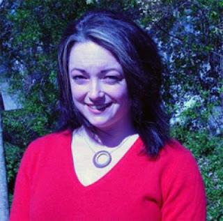
Qun Huo, University of Central Florida

Caption: University of Central Florida researcher Qun "Treen" Huo works with gold nanoparticles.

Credit: Jacque Brund. Usage Restrictions: None.
Prostate cancer affects one of every six men and is the second-most common cancer among men in the United States, according to the American Cancer Society. It is estimated that more than 2 million American men are currently living with prostate cancer and that one new case occurs every 2.7 minutes. More than 27,000 men die from the disease each year, according to the American Cancer Society.
Huo and her team at the UCF lab developed the new technique involving gold nanoparticles, which she first mixes in a solution. The nanoparticles are engineered to attach themselves to cancer-producing proteins related to the type of cancer she is targeting. When she places a drop of blood in the solution, the gold nanoparticles seek out the protein. If the protein is present, the gold nanoparticles cluster around it. Using a dynamic light-scattering instrument, she looks for the clusters. If there are no clusters, there is no cancer-causing protein.

During a test, if cancer-producing proteins are detected at a significant level, the consumer would be directed to see a doctor.

"Think of it like a pregnancy test," Huo said. "It's the same principle. Women use it to find out if they are pregnant, but once they see the results at home, they go to the doctor to be sure."

The cancer-related protein marker that the gold nanoparticles seek out in Huo's research is the same one screened for by the FDA-approved Prostate-Specific Antigen (PSA) test. The PSA has a good track record as a protein marker for detecting prostate cancer and has been used by physicians for years. Huo said her new technique is much more sensitive and accurate than the PSA and all current techniques used in diagnostic labs.

"What's different is the technology," Huo said. "It's very simple. The dynamic light-scattering technique is highly sensitive and can pick up even the smallest trace amount of protein markers."

That's why the technique also can help doctors track any resurgence of cancer once a surgery is performed to remove it.

Dr. Baker, director of M.D. Anderson-Orlando's Cancer Research Institute, collaborates with Huo by offering her expertise in cancer research and by providing human blood and serum samples to test Huo's technique.

"The excitement for us here at M. D. Anderson-Orlando is that we can easily test the validity of the technique in our cancer research program and then on our own patients in a clinical trial," Baker said. "We are optimistic that we can begin clinical trials with this test within the next two years."

Huo said that the technique is still years from commercialization, but that in three to five years an over-the-counter test kit for prostate cancer is likely. The technique also can be easily adapted to test for many different types of cancer – Huo plans to focus first on ovarian and breast cancer. ###

Huo, who joined UCF in 2005, is an associate professor at the NanoScience Technology Center and Department of Chemistry. She teaches and conducts research in nanomaterials chemistry and developing applications for nanoparticle materials. Her interest in cancer research stems from watching friends and relatives battle a variety of cancers with little warning because symptoms are difficult to detect. Much of her research is funded through the National Science Foundation.

UCF Stands For Opportunity --The University of Central Florida is a metropolitan research university that ranks as the 5th largest in the nation with more than 50,000 students. UCF's first classes were offered in 1968. The university offers impressive academic and research environments that power the region's economic development. UCF's culture of opportunity is driven by our diversity, Orlando environment, history of entrepreneurship and our youth, relevance and energy. For more information visit news.ucf.edu

M. D. Anderson Cancer Center Orlando, part of Orlando Health, is affiliated with The University of Texas M. D. Anderson Cancer Center in Houston. U.S. News & World Report recently ranked M. D. Anderson Cancer Center as the top cancer treatment center in the U.S. and has ranked it as one of the top two cancer centers for the past 13 years. Orlando Health, a 1,780-bed community-owned, Florida not-for-profit organization established in 1918, annually serves nearly 2 million Central Florida residents and more than 4,500 international patients. More information is available at orlandohealth.com and mdacco.com.

Contact: Zenaida Gonzalez Kotala zkotala@mail.ucf.edu 407-823-6120 University of Central Florida

Tuesday, July 28, 2009

Evidence of macroscopic quantum tunneling detected in nanowires

CHAMPAIGN, Ill. — A team of researchers at the University of Illinois has demonstrated that, counter to classical Newtonian mechanics, an entire collection of superconducting electrons in an ultrathin superconducting wire is able to "tunnel" as a pack from a state with a higher electrical current to one with a notably lower current, providing more evidence of the phenomenon of macroscopic quantum tunneling.

Physics professors Alexey Bezryadin and Paul Goldbart led the team, with graduate student Mitrabhanu Sahu performing the bulk of the measurements. Their research was published on the Web site of the journal Nature Physics on May 17.

Quantum tunneling is the capability of a particle to inhabit regions of space that would normally be off-limits according to classical mechanics.

Bezryadin Group

Caption: Physics professors Alexey Bezryadin, left, and Paul Goldbart flank graduate student Mitrabhanu Sahu, who performed the bulk of the measurements.

Credit: L. Brian Stauffer. Usage Restrictions: None.
This research observes a process called a quantum phase slip, whereby packs of roughly 100,000 electrons tunnel together from higher electrical current states to lower ones. The energy locked in the motion of the electrons as they phase slip is dissipated as heat, causing the nanowires to switch from a superconducting state to a more highly resistive one.

It's through this switching of states that allows the tunneling of the phase slip to be observed, the researchers say.
Goldbart, who is also a researcher at the university's Frederick Seitz Materials Research Laboratory, describes a quantum phase slip as a phenomenon that allows the spatially extended structure of superconductivity "to undergo a kind of quantum mechanical rip or tear, one where the entire extended behavior of the superconductivity tunnels its way through a classically forbidden set of configurations."

"Semiconductors, insulators and metals all hinge upon the ability of particles to make it through classically forbidden regions, despite apparently having negative kinetic energy there, as quantum physics allows," Goldbart said.

In Newton's world, according to Goldbart, particles would be reflected from such regions.

Although quantum mechanics governs the realm of atoms and molecules and smaller, quantum phenomena sometimes "leak up" to macroscopic scales, he said.

The ultrathin superconducting nanowires fabricated and measured by Sahu and his co-researchers are about 2,000 times finer than a single strand of human hair, which is still "a substantially larger scale than where one typically expects to observe quantum tunneling," Bezryadin said.

According to Bezryadin, who is also a researcher at the Beckman Institute and the Illinois Micro and Nanotechnology Laboratory, it has long been established that single electrons can tunnel, but scant evidence has existed until now for the group tunneling of a large ensemble of superconducting electrons confined in a thin wire.

"Observing switching events in superconducting nanowires at high-bias currents provides strong evidence for quantum phase slips," Bezryadin said. "Our experiments provide further evidence that the laws of quantum mechanics continue to govern large systems, composed of many thousands of electrons, acting as a single entity."

Both researchers believe that the practical implication of knowledge gleaned from research into quantum tunneling could have applications in the field of quantum computing.

"If we learn how to evade the factors that currently suppress quantum superpositions at the macro-scale," Bezryadin said, "we would be better positioned to construct quantum bits for quantum computers, which could perform tasks with an enormous increase in speed and security." ###

Funding for this research was provided by the U.S. Department of Energy through the Frederick Seitz Materials Research Laboratory and the Institute for Condensed Matter Theory, both at the University of Illinois.

Editor's note: To contact Alexey Bezryadin, call 217-333-9580; e-mail: bezryadi@illinois.edu.Paul Goldbart: 217-333-1195; goldbart@illinois.edu.

Contact: Phil Ciciora pciciora@illinois.edu 217-333-2177 University of Illinois at Urbana-Champaign

Sunday, July 26, 2009

Multiferroics -- making a switch the electric way

BERKELEY, CA – Multiferroics are materials in which unique combinations of electric and magnetic properties can simultaneously coexist. They are potential cornerstones in future magnetic data storage and spintronic devices provided a simple and fast way can be found to turn their electric and magnetic properties on and off. In a promising new development, researchers with the U.S. Department of Energy's Lawrence Berkeley National Laboratory (Berkeley Lab) working with a prototypical multiferroic have successfully demonstrated just such a switch -- electric fields.

"Using electric fields, we have been able to create, erase and invert p–n junctions in a calcium-doped bismuth ferrite film," said Ramamoorthy Ramesh of Berkeley Lab's Materials Sciences Division (MSD), who led this research.

"Through the combination of electronic conduction with the electric and magnetic properties already present in the multiferroic bismuth ferrite, our demonstration opens the door to merging magnetoelectrics and magnetoelectronics at room temperature."

Ramamoorthy Ramesh and Chan-Ho Yang

Caption: Ramamoorthy Ramesh and Chan-Ho Yang of Berkeley Lab's Materials Sciences Division successfully demonstrated that electric fields can be used as ON/OFF switches in doped multiferroic films, a development that holds promise for future magnetic data storage and spintronic devices.

Credit: Photograph by Roy Kaltschmidt, Berkeley Lab Public Affairs. Usage Restrictions: None.
Ramesh, who is also a professor in the Department of Materials Science and Engineering and the Department of Physics at UC Berkeley, has published a paper on this research that is now available in the on-line edition of the journal Nature Materials. The paper is titled: "Electric modulation of conduction in multiferroic Ca-doped BiFeO3 films." Co-authoring the paper with Ramesh were Chan-Ho Yang, Jan Seidel,Sang-Yong Kim, Pim Rossen, Pu Yu, Marcin Gajek, Ying-Hao Chu, Lane Martin, Micky Holcomb, Qing He, Petro Maksymovych, Nina Balke, Sergei Kalinin, Arthur Baddorf, Sourav Basu and Matthew Scullin.
The next generation of computers promises to be smaller, faster and far more versatile than today's devices thanks in part to the anticipated development of memory chips that store data through electron spin and its associated magnetic moment rather than electron charge. Because multiferroics simultaneously exhibit two or more ferro electric or magnetic properties in response to changes in their environment, they're considered prime candidates to be the materials of choice for this technology.

Bismuth ferrite is a multiferroic comprised of bismuth, iron and oxygen (BiFeO3). It is both ferroelectric and antiferromagnetic ("ferro" refers to magnetism in iron but the term has grown to include materials and properties that have nothing to do with iron), and has commanded particular interest in the spintronics field, especially after a surprising discovery by Ramesh and his group earlier this year. They found that although bismuth ferrite is an insulating material, running through its crystals are ultrathin (two-dimensional) sheets called "domain walls" that conduct electricity at room temperature. This discovery suggested that with the right doping, the conducting states in bismuth ferrite could be stabilized, opening the possibility of creating p-n junctions, a crucial key to solid state electronics.
"Insulator to conductor transitions are typically controlled through the combination of chemical doping and magnetic fields but magnetic fields are too expensive and energy-consuming to be practical in commercial devices," said Ramesh. "Electric fields are much more useful control parameters because you can easily apply a voltage across a sample and modulate it as needed to induce insulator-conductor transitions."

In their new study, Ramesh and his group first doped the bismuth ferrite with calcium acceptor ions, which are known to increase the amount of electric current that materials like bismuth ferrite can carry. The addition of the calcium ions created positively-charged oxygen vacancies. When an electric field was applied to the calcium-doped bismuth ferrite films, the oxygen vacancies became mobile.

The electric field "swept" the oxygen vacancies towards the film's top surface, creating an n-type semiconductor in that portion of the film,
calcium-doped bismuth ferrite multiferroic

Caption: This image recorded after an electric field was applied to a calcium-doped bismuth ferrite multiferroic film shows in the top image current being conducted within the red rectangle (On). In the bottom image, an opposite electric field was applied to the area within the green rectangle, switching it back to an insulating state (Off).

Credit: image by Chan-Ho Yang, Berkeley Lab/UC Berkeley. Usage Restrictions: None.
while the immobile calcium ions created a p-type semiconductor in the bottom portion. Reversing the direction of the electric field inverted the n-type and p-type semiconductor regions, and a moderate field erased them.

"It is the same principle as in a CMOS device where the application of a voltage serves as an on/off switch that controls electron transport properties and changes electrical resistance from high (insulator) to low (conductor)," said Ramesh.

Whereas a typical CMOS device features an on/off switching ratio (the difference between resistance and non-resistance to electrical current) of about one million, Ramesh and his group achieved an on/off switching ratio of about a thousand in their calcium-doped bismuth ferrite films. While this ratio is sufficient for device operation and double the best ratio achieved with magnetic fields, Chan-Ho Yang, lead author on this Nature Materials paper and a post-doc in Ramesh's group says it can be improved.

"To make the ON state more conductive, we have many ideas to try such as different calcium-doping ratios, different strain states, different growth conditions, and eventually different compounds using the same idea," Yang said.

A year ago, Ramesh and his group demonstrated that an electric field could be used to control ferromagnetism in a non-doped bismuth ferrite film. (See Nature Materials, "Electric-field control of local ferromagnetism using a magnetoelectric multiferroic" by Ramesh, et. al)

With this new demonstration that the combination of doping and an applied electric field can change the insulating-conducting state of a multiferroic, he and his colleagues have shown one way forward in adapting multiferroics to such phenomena as colossal magnetoresistance, high temperature superconductivity and SQUID-type magnetic field detectors as well as spintronics.

Said Yang, "Oxides such as bismuth ferrite are abundant and display many exotic properties including high-temperature superconductivity and colossal magnetoresistance, but they have not been used much in real applications because it has been so difficult to control defects, especially, oxygen vacancies. Our observations suggest a general technique to make oxygen vacancy defects controllable."

Much of the work in this latest study by Ramesh and his group was carried out at Berkeley Lab's Advanced Light Source (ALS), on the PEEM2 microscope. PEEM, which stands for PhotoEmission Electron Microscopy, is an ideal technique for studying ferro magnetic and antimagnetic domains, and PEEM2, powered by a bend magnet at ALS beamline 7.3.1.1, is one of the world's best instruments, able to resolve features only a few nanometers thick.

"Without the capabilities of PEEM2 our experiments would have been dead in the water," said Ramesh. "Andreas Scholl (who manages PEEM2) and his ALS team were an enormous help." ###

This research was primarily supported by the U.S. Department of Energy's Office of Science through its Basic Energy Sciences program.

Berkeley Lab is a U.S. Department of Energy national laboratory located in Berkeley, California. It conducts unclassified scientific research and is managed by the University of California. Visit our Website at www.lbl.gov

Contact: Lynn Yarris lcyarris@lbl.gov 510-486-5375 DOE/Lawrence Berkeley National Laboratory

Friday, July 24, 2009

New 'broadband' cloaking technology simple to manufacture

WEST LAFAYETTE, Ind. - Researchers have created a new type of invisibility cloak that is simpler than previous designs and works for all colors of the visible spectrum, making it possible to cloak larger objects than before and possibly leading to practical applications in "transformation optics."

Whereas previous cloaking designs have used exotic "metamaterials," which require complex nanofabrication, the new design is a far simpler device based on a "tapered optical waveguide," said Vladimir Shalaev, Purdue University's Robert and Anne Burnett Professor of Electrical and Computer Engineering.

Waveguides represent established technology - including fiber optics - used in communications and other commercial applications.

New Type of Invisibility Cloak

Caption: This image shows the design of a new type of invisibility cloak that is simpler than previous designs and works for all colors of the visible spectrum, making it possible to cloak larger objects than before and possibly leading to practical applications in "transformation optics."

Credit: Purdue University. Usage Restrictions: None.
The research team used their specially tapered waveguide to cloak an area 100 times larger than the wavelengths of light shined by a laser into the device, an unprecedented achievement. Previous experiments with metamaterials have been limited to cloaking regions only a few times larger than the wavelengths of visible light.

Because the new method enabled the researchers to dramatically increase the cloaked area, the technology offers hope of cloaking larger objects, Shalaev said.

Findings are detailed in a research paper appearing May 29 in the journal Physical Review Letters.
The paper was written by Igor I. Smolyaninov, a principal electronic engineer at BAE Systems in Washington, D.C.; Vera N. Smolyaninova, an assistant professor of physics at Towson University in Maryland; Alexander Kildishev, a principal research scientist at Purdue's Birck Nanotechnology Center; and Shalaev.

"All previous attempts at optical cloaking have involved very complicated nanofabrication of metamaterials containing many elements, which makes it very difficult to cloak large objects," Shalaev said. "Here, we showed that if a waveguide is tapered properly it acts like a sophisticated nanostructured material."

The waveguide is inherently broadband, meaning it could be used to cloak the full range of the visible light spectrum. Unlike metamaterials, which contain many light-absorbing metal components, only a small portion of the new design contains metal.

Theoretical work for the design was led by Purdue, with BAE Systems leading work to fabricate the device, which is formed by two gold-coated surfaces, one a curved lens and the other a flat sheet. The researchers cloaked an object about 50 microns in diameter, or roughly the width of a human hair, in the center of the waveguide.

"Instead of being reflected as normally would happen, the light flows around the object and shows up on the other side, like water flowing around a stone," Shalaev said.

The research falls within a new field called transformation optics, which may usher in a host of radical advances, including cloaking; powerful "hyperlenses" resulting in microscopes 10 times more powerful than today's and able to see objects as small as DNA; computers and consumer electronics that use light instead of electronic signals to process information; advanced sensors; and more efficient solar collectors.

Unlike natural materials, metamaterials are able to reduce the "index of refraction" to less than one or less than zero. Refraction occurs as electromagnetic waves, including light, bend when passing from one material into another. It causes the bent-stick-in-water effect, which occurs when a stick placed in a glass of water appears bent when viewed from the outside. Each material has its own refraction index, which describes how much light will bend in that particular material and defines how much the speed of light slows down while passing through a material.

Natural materials typically have refractive indices greater than one. Metamaterials, however, can be designed to make the index of refraction vary from zero to one, which is needed for cloaking.

The precisely tapered shape of the new waveguide alters the refractive index in the same way as metamaterials, gradually increasing the index from zero to 1 along the curved surface of the lens, Shalaev said.

Previous cloaking devices have been able to cloak only a single frequency of light, meaning many nested devices would be needed to render an object invisible.

Kildishev reasoned that the same nesting effect might be mimicked with the waveguide design. Subsequent experiments and theoretical modeling proved the concept correct.

Researchers do not know of any fundamental limit to the size of objects that could be cloaked, but additional work will be needed to further develop the technique.

Recent cloaking findings reported by researchers at other institutions have concentrated on a technique that camouflages features against a background. This work, which uses metamaterials, is akin to rendering bumps on a carpet invisible by allowing them to blend in with the carpet, whereas the Purdue-based work concentrates on enabling light to flow around an object. ###

Related Web site: Vladimir Shalaev : https://engineering.purdue.edu/

Abstract on the research in this release is available at: http://news.uns.purdue.edu/

Contact: Emil Venere venere@purdue.edu 765-494-4709 Purdue University

Wednesday, July 22, 2009

Novel approach estimates nanoparticles in environment

DURHAM, N.C. – Without knowing how much of an industrial chemical is being produced, it is almost impossible for scientists to determine if it poses any threat to the environment or human health.

Civil engineers at Duke University believe they have come up with a novel way of estimating how much of one such material – titanium dioxide – is being generated, laying the groundwork for future studies to assess any possible risks.

This information is especially valuable if the chemicals are in the form of nano-particles, which possess unique properties because of their miniscule size. Nanoparticles are attractive for a wide range of products, little is known about their consequences in the environment.

Christine Robichaud, Duke University

Caption: This is Christine Robichaud from Duke University. Credit: Duke University. Usage Restrictions: None.

Mark Wiesner, Duke University

Caption: This is Mark Wiesner from Duke University. Credit: Duke University Photography. Usage Restrictions: None.

Bulk Titanium Dioxide

Caption: This is bulk titanium dioxide. Credit: Duke University. Usage Restrictions: None.
One of the most widely used is the nanoparticle form of titanium dioxide, which can be found in such diverse products as sunscreens and toothpaste to paints and papers. It is also used in water treatment.

"The biggest problem we face in trying to determine any risks of titanium dioxide nanoparticles is that no one really knows how much of it there is," said Christine Robichaud, graduate student in civil and environmental engineering at Duke's Pratt School of Engineering. The results of her analysis were published online in the Journal of Environmental Science and Technology.

Robichaud found it especially difficult trying to collect this data, since the companies that process titanium dioxide were not willing to reveal information they deemed proprietary. So she used a novel approach developed by collaborators Lynne Zucker and Michael Darby at the University of California Los Angeles to estimate the rate of innovation in the biotechnology industry.

"We combined science and engineering knowledge with business and economic modeling to come up with what we think is the maximum amount of titanium dioxide nanoparticles out there," Robichaud said. "By taking the amount of bulk titanium dioxide produced, which is better understood, and applying the rates of new technologies to convert it to the nanoparticle form found in journal articles and patent applications, we estimated the maximum ceiling amount."

Based on her calculations, Robichaud found that the production of titanium dioxide nanoparticles was negligible in 2002 and rose to about 2.5 percent of the total amount of titanium dioxide produced today.
By 2015, nanoparticle production is estimated to be about 10 percent of the total, as more companies switch to newer technology. Under the most aggressive scenario, practically all of titanium dioxide in the U.S., about 2.5 million metric tons, would be in nanoparticle form by 2025, Robichaud concluded.

"Knowing the amount of this material is important because the more of it we make, the more likely it is to enter the environment and come into contact with humans with unknown consequences," said Mark Wiesner, professor of civil and environmental engineering and senior member of the research team. He also directs the federally funded Center for the Environmental Implications of NanoTechnology (CEINT), which is based at Duke.

"We do not have a good handle on how much is out there, and even less about what that might mean," he continued. "Finding an upper limit on the potential for exposure is the critical first step in assessing risk. Even if these nanoparticles are toxic, a low exposure to them may limit the risk. We just don't know yet. I like to use the example of sharks. Everyone knows they're dangerous, but not if you spend your entire life in Nebraska."

Now that the researchers have a better idea how much of this nanomaterial could be produced in the coming years, they plan to focus on specific types of products.

"We want to get a better idea of where in the process these nanoparticles might be released into the air, water or soil," Robichaud said. "It could be during mining, during the production of the nanoparticles, production of the specific product using the nanoparticles, the use of the product, or its ultimate disposal." ###

The research was funded by National Science Foundation and CEINT. Other members of the team, from Duke, are Ali Emre Uyar, Michael Darby and Lynne Zucker.

Contact: Richard Merritt richard.merritt@duke.edu 91-906-608-414 Duke University

Monday, July 20, 2009

New Nanodiamond Tool for Next-Generation Cancer Treatments

EVANSTON, Ill. --- A research team at Northwestern University has demonstrated a tool that can precisely deliver tiny doses of drug-carrying nanomaterials to individual cells.

The tool, called the Nanofountain Probe, functions in two different ways: in one mode, the probe acts like a fountain pen, wherein drug-coated nanodiamonds serve as the ink, allowing researchers to create devices by “writing” with it. The second mode functions as a single-cell syringe, permitting direct injection of biomolecules or chemicals into individual cells.

The research was led by Horacio Espinosa, professor of mechanical engineering, and Dean Ho, assistant professor of mechanical and biomedical engineering, both at the McCormick School of Engineering and Applied Science at Northwestern. Their results were recently published online in the scientific journal Small.

Horacio Espinosa

Horacio Espinosa
The probe could be used both as a research tool in the development of next-generation cancer treatments and as a nanomanufacturing tool to build the implantable drug delivery devices that will apply these treatments. The potential of nanomaterials to revolutionize drug delivery is emergent in early trials, which show their ability to moderate the release of highly toxic chemotherapy drugs and other therapeutics. This provides a platform for drug-delivery schemes with reduced side effects and improved targeting.
“This is an exciting development that complements our previous demonstrations of direct patterning of DNA, proteins and nanoparticles,” says Espinosa.

Using the Nanofountain Probe, the group injected tiny doses of nanodiamonds into both healthy and cancerous cells. This technique will help cancer researchers investigate the efficacy of new drug-nanomaterial systems as they become available.

The group also used the same Nanofountain Probes to pattern dot arrays of drug-coated nanodiamonds directly on glass substrates. The production of these dot arrays, with dots that can be made smaller than 100 nanometers in diameter, provides the proof of concept by which to manufacture devices that will deliver these nanomaterials within the body.

The work addresses two major challenges in the development and clinical application of nanomaterial-mediated drug-delivery schemes: dosage control and high spatial resolution.

In fundamental research and development, biologists are typically constrained to studying the effects of a drug on an entire cell population because it is difficult to deliver them to a single cell. To address this issue, the team used the Nanofountain Probe to target and inject single cells with a dose of nanodiamonds.

“This allows us to deliver a precise dose to one cell and observe its response relative to its neighbors,” Ho says. “This will allow us to investigate the ultimate efficacy of novel treatment strategies via a spectrum of internalization mechanisms.”

Beyond the broad research focused on developing these drug-delivery schemes, manufacturing devices to execute the delivery will require the ability to precisely place doses of drug-coated nanomaterials. Ho and colleagues previously developed a polymer patch that could be used to deliver chemotherapy drugs locally to sites where cancerous tumors have been removed. This patch is embedded with a layer of drug-coated nanodiamonds, which moderate the release of the drug. The patch is capable of controlled and sustained low levels of release over a period of months, reducing the need for chemotherapy following the removal of a tumor.

“An attractive enhancement will be to use the Nanofountain Probe to replace the continuous drug-nanodiamond films currently used in these devices with patterned arrays composed of multiple drugs,” Ho says. “This allows high-fidelity spatial tuning of dosing in intelligent devices for comprehensive treatment.”

“One of the most significant aspects of this work is the Nanofountain Probe’s ability to deliver nanomaterials coated with a broad range of drugs and other biological agents,” Espinosa says. “The injection technique is currently being explored for delivery of a wide variety of bio-agents, including DNA, viruses and other therapeutically relevant materials.”

Nanodiamonds have also proven effective in seeding the growth of diamond thin films. These diamond films have exciting applications in next-generation nanoelectronics. Here again, the ability to pattern nanodiamonds with sub-100-nanometer resolution provides inroads to realizing these devices on a mass scale. The resolution in nanodiamond patterning demonstrated by the Nanofountain Probe represents an improvement of three orders of magnitude over other reported direct-write schemes of nanodiamond patterning.

The work was supported by the National Science Foundation, the National Institutes of Health, the V Foundation for Cancer Research and the Wallace H. Coulter Foundation.

In addition to Espinosa and Ho, other authors of the paper, entitled “Nanofountain Probe-based High-resolution Patterning and Single-cell Injection of Functionalized Nanodiamonds,” are Owen Loh, Robert Lam, Mark Chen, Nicolaie Moldovan and Houjin Huang of Northwestern University.

Contact: Kyle Delaney k-delaney@northwestern.edu 847-467-4010 Northwestern University

Sunday, July 19, 2009

New element found to be a superconductor

New element found to be a superconductor. Of the 92 naturally occurring elements, add another to the list of those that are superconductors.

James S. Schilling, Ph.D., professor of physics in Arts & Sciences at Washington University in St. Louis, and Mathew Debessai, Ph.D., — his doctoral student at the time — discovered that europium becomes superconducting at 1.8 K (-456 °F) and 80 GPa (790,000 atmospheres) of pressure, making it the 53rd known elemental superconductor and the 23rd at high pressure.

Debessai, who received his doctorate in physics at Washington University's Commencement May 15, 2009, is now a postdoctoral research associate at Washington State University.

diamond cell

Inside of the diamond cell: In the middle is the coil system around the diamond anvil, which picks up the shielding signal from the superconducting sample.
"It has been seven years since someone discovered a new elemental superconductor," Schilling said. "It gets harder and harder because there are fewer elements left in the periodic table."

This discovery adds data to help improve scientists' theoretical understanding of superconductivity, which could lead to the design of room-temperature superconductors that could be used for efficient energy transport and storage.
The results are published in the May 15, 2009, issue of Physical Review Letters in an article titled "Pressure-induced Superconducting State of Europium Metal at Low Temperatures."

Schilling's research is supported by a four-year $500,000 grant from the National Science Foundation, Division of Materials Research.

Europium belongs to a group of elements called the rare earth elements. These elements are magnetic; therefore, they are not superconductors.

"Superconductivity and magnetism hate each other. To get superconductivity, you have to kill the magnetism," Schilling explained.

Of the rare earths, europium is most likely to lose its magnetism under high pressures due to its electronic structure. In an elemental solid almost all rare earths are trivalent, which means that each atom releases three electrons to conduct electricity.

"However, when europium atoms condense to form a solid, only two electrons per atom are released and europium remains magnetic. Applying sufficient pressure squeezes a third electron out and europium metal becomes trivalent. Trivalent europium is nonmagnetic, thus opening the possibility for it to become superconducting under the right conditions," Schilling said.

Schilling uses a diamond anvil cell to generate such high pressures on a sample. A circular metal gasket separates two opposing 0.17-carat diamond anvils with faces (culets) 0.18 mm in diameter. The sample is placed in a small hole in the gasket, flanked by the faces of the diamond anvils.

Pressure is applied to the sample space by inflating a doughnut-like bellow with helium gas. Much like a woman in stilettos exerts more pressure on the ground than an elephant does because the woman's force is spread over a smaller area, a small amount of helium gas pressure (60 atmospheres) creates a large force (1.5 tons) on the tiny sample space, thus generating extremely high pressures on the sample.

Unique electrical, magnetic properties

Superconducting materials have unique electrical and magnetic properties. They have no electrical resistance, so current will flow through them forever, and they are diamagnetic, meaning that a magnet held above them will levitate.

These properties can be exploited to create powerful magnets for medical imaging, make power lines that transport electricity efficiently or make efficient power generators.

However, there are no known materials that are superconductors at room temperature and pressure. All known superconducting materials have to be cooled to extreme temperatures and/or compressed at high pressure.

"At ambient pressure, the highest temperature at which a material becomes superconducting is 134 K (-218 °F). This material is complex because it is a mixture of five different elements. We do not understand why it is such a good superconductor," Schilling said.

Scientists do not have enough theoretical understanding to be able to design a combination of elements that will be superconductors at room temperature and pressure. Schilling's result provides more data to help refine current theoretical models of superconductivity.

"Theoretically, the elemental solids are relatively easy to understand because they only contain one kind of atom," Schilling said. "By applying pressure, however, we can bring the elemental solids into new regimes, where theory has difficulty understanding things.

"When we understand the element's behavior in these new regimes, we might be able to duplicate it by combining the elements into different compounds that superconduct at higher temperatures."

Schilling will present his findings at the 22nd biennial International Conference on High Pressure Science and Technology in July 2009 in Tokyo, Japan.

Contact: James S. Schilling jss@wuphys.wustl.edu 314-935-6239 Washington University in St. Louis

Friday, July 17, 2009

Inexpensive plastic used in CDs could improve aircraft, computer electronics

Physics professor at UH uses Air Force grants to create highly conductive nanocomposites

HOUSTON, – If one University of Houston professor has his way, the inexpensive plastic now used to manufacture CDs and DVDs will one day soon be put to use in improving the integrity of electronics in aircraft, computers and iPhones.

Thanks to a pair of grants from the U.S. Air Force, Shay Curran, associate professor of physics at UH, and his research team have demonstrated ultra-high electrical conductive properties in plastics, called polycarbonates, by mixing them with just the right amount and type of carbon nanotubes.

Shay Curran

Shay Curran
The findings are chronicled in a paper titled "Electrical Transport Measurements of Highly Conductive Carbon Nanotube/Poly(bisphenol A carbonate) Composite," appearing in a recent issue of the Journal of Applied Physics, the archival publication of the American Institute of Physics for significant new results in the field.

Curran, who initially began this form of research a decade ago at Trinity College Dublin, started to look at high-conductive plastics in a slightly different manner.
Curran's team has come up with a strategy to achieve higher conductivities using carbon nanotubes in plastic hosts than what has been currently achieved. By combining nanotubes with polycarbonates, Curran's group was able to reach a milestone of creating nanocomposites with ultra-high conductive properties.

"While its mechanical and optical properties are very good, polycarbonate is a non-conductive plastic. That means its ability to carry an electrical charge is as good as a tree, which is pretty awful," Curran said. "Imagine that this remarkable plastic can now not only have good optical and mechanical properties, but also good electrical characteristics. By being able to tailor the amount of nanotubes we can add to the composite, we also can change it from the conductivity of silicon to a few orders below that achieved by metals."

Making this very inexpensive plastic highly conductive could benefit electronics in everything from military aircraft to personal computers. Computer failure, for instance, results from the build up of thermal and electrical charges, so developing these polymer nanotube composites into an antistatic coating or to provide a shield against electromagnetic interference would increase the lifespan of computing devices, ranging from PCs to PDAs.

The next step of this research is to develop ink formulations to paint these polycarbonate nanocomposites onto various electrical components. Normally, metal plates are used to dissipate electrical charge, so it's not surprising that the availability of a paintable ink would be particularly appealing to the Air Force for its lightweight properties, resulting in lighter aircraft that guzzle less gas.

Another key component of this latest research is that pristine nanotubes disbursed in this polycarbonate were found to possess an even higher conductivity than acid-treated carbon nanotubes. Traditionally, the tubes are sonicated, or treated with acid, to clean them and remove soot to get a higher conductivity. This, however, damages the tubes and exposes them to defects. Instead, Curran and his group were able to centrifuge, or swirl, them. This takes a little longer, but increases the potential to have higher conductivities. He attributes this to the incredibly clean samples of carbon nanotubes obtained from fellow collaborator David Carroll in the physics department at Wake Forest University.

In addition to Curran and Carroll, the team behind these remarkable findings includes Donald Birx, professor of electrical engineering and vice president for research at UH, two of Curran's former post-doctoral students, Jamal Talla and Donghui Zhang, and a current Curran student, Sampath Dias.

Coincidentally, Curran's former thesis supervisor Werner Blau and his group in the department of physics at Trinity College Dublin have come out with similar findings recently in the journal ACS Nano. Both groups really have been pushing hard in the area of polymer nanotube composites during the course of the last decade. Curran said his group at UH achieved the highest conductivity levels so far, but also is encouraged by Blau's success and said repeating these types of outcomes will open doors for even higher values.

"While these are phenomenal results, finding these unusual highly conductive properties has not even begun to scratch the surface," Curran said. "There is hard science behind it, so developing it further will require significant investment. And we are very thankful to the Air Force for giving us this auspicious start." ###

About the University of Houston

The University of Houston, Texas' premier metropolitan research and teaching institution, is home to more than 40 research centers and institutes and sponsors more than 300 partnerships with corporate, civic and governmental entities. UH, the most diverse research university in the country, stands at the forefront of education, research and service with more than 36,000 students.

About the College of Natural Sciences and Mathematics

The UH College of Natural Sciences and Mathematics, with nearly 400 faculty members and approximately 4,000 students, offers bachelor's, master's and doctoral degrees in the natural sciences, computational sciences and mathematics. Faculty members in the departments of biology and biochemistry, chemistry, computer science, geosciences, mathematics and physics have internationally recognized collaborative research programs in association with UH interdisciplinary research centers, Texas Medical Center institutions and national laboratories.

Contact: Lisa Merkl lkmerkl@uh.edu 713-743-8192 University of Houston

Wednesday, July 15, 2009

Graphene Yields Secrets to Its Extraordinary Properties

Applying innovative measurement techniques, researchers from the Georgia Institute of Technology and the National Institute of Standards and Technology (NIST) have directly measured the unusual energy spectrum of graphene, a technologically promising, two-dimensional form of carbon that has tantalized and puzzled scientists since its discovery in 2004.

Published in this week’s issue of Science,* their work adds new detail to help explain the unusual physical phenomena and properties associated with graphene, a single layer of carbon atoms arrayed in a repeating, honeycomb-like arrangement.

Graphene’s exotic behaviors present intriguing prospects for future technologies, including high-speed, graphene-based electronics that might replace today’s silicon-based integrated circuits and other devices. Even at room temperature, electrons in graphene are more than 100 times more mobile than in silicon.

atomic contours of graphene

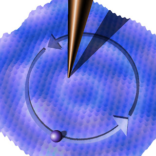
Drawing represents a probe scanning and mapping the atomic contours of graphene, a single layer of carbon atoms arranged in a honeycomb-like array. Simultaneously applying a magnetic field causes electrons (ball) to organize in circular orbits, like a dog chasing its tail. Orbits hold clues to the material's exotic properties. Credit: NIST.

graphene's honeycomb structure

NIST-built STM "shuttle" module contains the atomic-scale position-and-scan system. Graphene sample and probe tip are in the center opening. Shuttle moves between a room-temperature vacuum environment for loading to an ultracold environment for measuring. Model in background shows graphene's honeycomb structure. Credit: NIST
Graphene apparently owes this enhanced mobility to the curious fact that its electrons and other carriers of electric charges behave as though they do not have mass. In conventional materials, the speed of electrons is related to their energy, but not in graphene. Although they do not approach the speed of light, the unbound electrons in graphene behave much like photons, massless particles of light that also move at a speed independent of their energy.

This weird massless behavior is associated with other strangeness. When ordinary conductors are put in a strong magnetic field, charge carriers such as electrons begin moving in circular orbits that are constrained to discrete, equally spaced energy levels. In graphene these levels are known to be unevenly spaced because of the “massless” electrons.

The Georgia Tech/NIST team tracked these massless electrons in action, using a specialized NIST instrument to zoom in on the graphene layer at a billion times magnification, tracking the electronic states while at the same time applying high magnetic fields. The custom-built, ultra-low-temperature and ultra-high-vacuum scanning tunneling microscope allowed them to sweep an adjustable magnetic field across graphene samples prepared at Georgia Tech, observing and mapping the peculiar non-uniform spacing among discrete energy levels that form when the material is exposed to magnetic fields.
The team developed a high-resolution map of the distribution of energy levels in graphene. In contrast to metals and other conducting materials, where the distance from one energy peak to the next is uniformly equal, this spacing is uneven in graphene.

The researchers also probed and spatially mapped graphene’s hallmark “zero energy state,” a curious phenomenon where the material has no electrical carriers until a magnetic field is applied.

The measurements also indicated that layers of graphene grown and then heated on a substrate of silicon-carbide behave as individual, isolated, two-dimensional sheets. On the basis of the results, the researchers suggest that graphene layers are uncoupled from adjacent layers because they stack in different rotational orientations. This finding may point the way to manufacturing methods for making large, uniform batches of graphene for a new carbon-based electronics.

The research was funded in part by the National Science Foundation, W. M. Keck Foundation, and Semiconductor Research Corporation through the Nanoelectronics Research Initiative INDEX program, which NIST also supports.

* D.L. Miller, K.D. Kubista, G.M. Rutter, M. Ruan, W.A. de Heer, P.N. First and J.A. Stroscio. Observing the quantization of zero mass carriers in graphene. Science. May 15, 2009.

Contact: Mark Bello mark.bello@nist.gov 301-975-3776 National Institute of Standards and Technology (NIST)

Tuesday, July 14, 2009

New fuel cell catalyst uses 2 metals

More efficient than commercial catalysts

Material scientists at Washington University in St. Louis have developed a technique for a bimetallic fuel cell catalyst that is efficient, robust and two to five times more effective than commercial catalysts. The novel technique eventually will enable a cost effective fuel cell technology, which has been waiting in the wings for decades, and should give a boost for cleaner use of fuels worldwide.

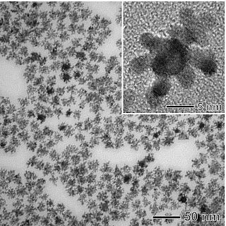
Younan Xia, Ph.D., the James M. McKelvey Professor of Biomedical Engineering at Washington University led a team of scientists at Washington University and the Brookhaven National Laboratory in developing a bimetallic catalyst comprised of a palladium core or "seed" that supports dendritic platinum branches, or arms, that are fixed on the nanostructure, consisting of a nine nanometer core and seven nanometer platinum arms.

new catalyst based on dendritic platinum arm

A new catalyst based on dendritic platinum arms grown on palladium nanocrystals has been developed by WUSTL's Younan Xia and his collaborators. Tests have shown that the "bimetallic" catalyst outperforms commercial catalysts, which could enable a cost effective fuel cell technology and ultimately provide cleaner fuels worldwide.
They synthesized the catalysts by sequentially reducing precursor compounds to palladium and platinum with L-ascorbic acid (that is, Vitamin C) in an aqueous solution. The catalysts have a high surface area, invaluable for a number of applications besides in fuel cells, and are robust and stable.

Xia and his team tested how the catalysts performed in the oxygen reduction reaction process in a fuel cell, which determines how large a current will be generated in an electrochemical system similar to the cathode of a fuel cell. They found that their bimetallic nanodendrites, at room temperature, were two-and-a-half times more effective per platinum mass for this process than the state-of-the-art commercial platinum catalyst and five times more active than the other popular commercial catalyst.
At 60 C(the typical operation temperature of a fuel cell), the performance almost meets the targets set by the U.S. Department of Energy.

The Department of Energy has estimated for widespread commercial success the "loading" of platinum catalysts in a fuel cell should be reduced by four times in order to slash the costs. The Washington University technique is expected to substantially reduce the loading of platinum, making a more robust catalyst that won't have to be replaced often, and making better use of a very limited and very expensive supply of platinum in the world.

"There are two ways to make a more effective catalyst," Xia says. "One is to control the size, making it smaller, which gives the catalyst a higher specific surface area on a mass basis. Another is to change the arrangement of atoms on the surface. We did both. You can have a square or hexagonal arrangement for the surface atoms. We chose the hexagonal lattice because people have found that it's twice as good as the square one for the oxygen reduction reaction.

"We're excited by the technique, specifically with the performance of the new catalyst."

Xia says seeded growth has emerged recently as a good technique for precisely controlling the shape and composition of metallic nanostructures prepared in solutions. And it's the only technique that allowed Xia and his collaborators to come up with their unconventional shape.

"When you have something this small, the atoms tend to aggregate and that can reduce the surface area,' Xia says. "A key reason our technique works is the ability to keep the platinum arms fixed. They don't move around. This adds to their stability. We also make sure of the arrangement of atoms on each arm, so we increase the activity."

Xia and his collaborators are exploring the possibility of adding other noble metals such as gold to the bimetallic catalysts, making them trimetallic. Gold has been shown to oxidize carbon monoxide, making for even more robust catalysts that can resist the poisoning by carbon monoxide – a reduction byproduct of some fuels.

"Gold should make the catalysts more stable, durable and robust, giving yet another level of control," Xia says. ###

Contact: Younan Xia xia.yunan@wustl.edu 314-935-8328 Washington University in St. Louis

Sunday, July 12, 2009

WPI professor receives Fulbright Scholarship to work on tissue engineering in Ireland

Biomedical engineering professor Kristen Billiar, who will study the mechanics of nanoscale scaffolds for tissue engineering at the National University of Ireland Galway, is the 14th member of the current WPI faculty to be named a Fulbright Scholar.

WORCESTER, Mass. – Kristen L. Billiar, associate professor of biomedical engineering at Worcester Polytechnic Institute (WPI), has been awarded a Fulbright Scholarship to work at the National University of Ireland Galway on research and education related to tissue engineering. Billiar, who will be in Ireland for the 2009-10 academic year, is the 14th member of the current WPI faculty to be awarded a Fulbright Scholar grant.

Kristen Billiar

Caption: This is Kristen L. Billiar, associate professor of biomedical engineering, Worcester Polytechnic Institute.

Credit: Worcester Polytechnic Institute. Usage Restrictions: None.
The Fulbright Program, the U.S. government's flagship program in international educational exchange, is sponsored by the United States Department of State, Bureau of Educational and Cultural Affairs. Each year, the traditional Fulbright Scholar Program sends 800 U.S. faculty members and other professionals abroad to lecture and conduct research in a wide variety of academic and professional fields.

"This significant honor is further evidence of the high quality of the WPI faculty and the important work they are doing through their research and scholarship," said John A. Orr, WPI's provost and senior vice president.
"This particular Fulbright Scholarship, the first for a current WPI researcher in the life sciences, is especially exciting as it demonstrates the value of the investment the university has made in research in this field in recent years, including the construction of the $50 million Life Sciences and Bioengineering Center at Gateway Park."

During his stay in Ireland, Billiar will study the mechanics of nanoscale scaffolds for tissue engineering with Dr. Abhay Pandit, Director of the Network of Excellence for Functional Biomaterials. Developing a detailed understanding of the relationship between the structure and mechanical functioning of connective tissue is critical to building engineered replacements for diseased tissue. In the research component of his Fulbright work, Billiar will seek to develop novel techniques for probing these relationships at the scale or nanometers, particularly as they relate to the scaffolds, or support structures, used in tissue engineering. He will also design inquiry-based biomechanics and biomaterials teaching laboratories based on these techniques and then compile them into a textbook.

Billiar joined the WPI faculty in 2002, after receiving a PhD in bioengineering at the University of Pennsylvania and working as a staff engineer at Organogenesis Inc. In his research he studies how the mechanical forces due to tissue stretching and cell contraction affect the growth and healing of soft tissue. His goal is to help make engineered skin, heart valves, and other tissues behave more naturally and reduce scarring during healing. His work has been supported by the Whittaker Foundation and the American Heart Association. In 2005, he received WPI's Romeo Moruzzi Young Faculty Award for Innovation in Undergraduate Education for developing a formal mentoring system to meet the challenge of providing experiential learning opportunities for students in his laboratory courses. H received the Trustee's Award for Academic Advising in 2008. ###

About Worcester Polytechnic Institute

Founded in 1865 in Worcester, Mass., WPI was one of the nation's first engineering and technology universities. WPI's14 academic departments offer more than 50 undergraduate and graduate degree programs in science, engineering, technology, management, the social sciences, and the humanities and arts, leading to bachelor's, master's and PhD degrees.

WPI's world-class faculty work with students in a number of cutting-edge research areas, leading to breakthroughs and innovations in such fields as biotechnology, fuel cells, and information security, materials processing, and nanotechnology.

Students also have the opportunity to make a difference to communities and organizations around the world through the university's innovative Global Perspective Program. There are more than 20 WPI project centers throughout North America and Central America, Africa, Australia, Asia, and Europe.

Contact: Michael Dorsey mwdorsey@wpi.edu 508-831-5609 Worcester Polytechnic Institute

Friday, July 10, 2009

UT nanomedicine project to be tested in space

Scientists win Microgravity Research Competition.

When a spacecraft launches from Cape Canaveral, Fla., in the future, its cargo will include a small box containing a nano-fluidics experiment designed by scientists at The University of Texas Health Science Center at Houston.

Investigators in the laboratory of Mauro Ferrari, Ph.D., nanomedicine division director at The UT Health Science Center at Houston, won a nationwide Microgravity Research Competition and with it the opportunity to test a research project aboard an extended flight of a SpaceX Falcon 9 rocket and Dragon spacecraft.

When sensors inside the box determine that near weightlessness has been achieved, the experiment will activate itself and begin a series of tests designed to learn more about the diffusion of micro nanoparticles through tiny microchannels measured in millionths of a meter, said Alessandro Grattoni, experiment project manager and senior research assistant in Ferrari's lab.

Mauro Ferrari, PhD.

Caption: Mauro Ferrari, Ph.D., is the nanomedicine division director at the University of Texas Health Science Center at Houston

Credit: Center for NanoMedicine Research at The University of Texas Health Science Center at Houston. Usage Restrictions: None.
Results of these experiments could aid in the development of implantable devices for controlled, long-term drug release. This research could yield important treatment means for illnesses, including cancer, said Grattoni, a Turin, Italy, native, who will receive his doctorate in biomedical engineering in May.

"I am delighted with this historic opportunity to perform research in space and bring back the results to Earth to improve health care," Ferrari said. "This experiment will allow us to refine our technologies for the release of a drug at the right time and to the right place in the body, and to bring to the clinic the vision of personalized medicine."

The competition was sponsored by The Heinlein Prize Trust, SpaceX (Space Exploration Technologies) and the Rice Alliance for Technology and Entrepreneurship. The trust is named after the late science fiction writer Robert Heinlein.
"World class experiments from The University of Texas Health Science Center at Houston teamed with the first cost effective laboratory in outer space from SpaceX will begin a new era of medical research for the 21st century. The commercial and health benefits to all of us will be immense," said Art Dula, trustee of the Heinlein Prize Trust.

In addition to the opportunity to test their experiment aboard SpaceX's Dragon spacecraft, the UT scientists received $25,000 and a trip to see the launch at Cape Canaveral. The proposal is titled "Decoupling Diffusive Transport Phenomena in Microgravity." ###
Arturas Ziemys and Alessandro Grattoni

Caption: UT nano scientists Arturas Ziemys, Ph.D., left, and Alessandro Grattoni are readying an experiment that will be tested in space.

Credit: Center for NanoMedicine Research at the University of Texas Health Science Center at Houston. Usage Restrictions: None.
UT nanomedicine team members include: Xuewu Liu, Ph.D., assistant professor, and post doctoral fellows Arturas Ziemys, Ph.D., Daniel Fine, Ph.D., and Enrica De Rosa, Ph.D.

For more information about the competition, visit www.labflight.com.

Contact: Robert Cahill Robert.Cahill@uth.tmc.edu 713-500-3042 University of Texas Health Science Center at Houston

Wednesday, July 08, 2009

University awarded £1.7M to develop nanotechnology for use in health care

Scientists at the University of Liverpool have been awarded £1.7 million to investigate how nanotechnology could be used to improve the effectiveness of pharmaceutical drugs.

Nanotechnology involves the manipulation of matter at sizes close to molecular level to produce particles that are small clusters of molecules. The collaborative project between the Departments of Chemistry and Pharmacology will apply nanotechnology techniques to develop new approaches for future drug development.

Many medicines currently in use have poor solubility and have to be administered in large doses to ensure that enough of the drug is absorbed into the body to be effective. Scientists, working closely with industry experts, will investigate the possibility of creating viable drugs in nanoparticle form – each particle being approximately 1/800th the width of a human hair. By examining how successfully they can be absorbed into the intestine, and in what form they pass into the bloodstream, they will also look to establish if nanotechnology can reduce the toxicity of drugs by using smaller doses without losing effect.

nanotechnology for use in healthcare

Scientists, working closely with industry experts, will investigate the possibility of creating viable drugs in nanoparticle form – each particle being approximately 1/800th the width of a human hair.
The project will focus on the HIV virus – the incurable disease that can lead to AIDS. There are more than 20 HIV medicines already on the market, which aim to prevent AIDS by ensuring that the disease cannot replicate uncontrollably in the body. It is important to maintain efficacy while avoiding excessively high or low doses that allow the development of resistance to the drugs. HIV drugs are a lifelong commitment and the doses currently needed have significant associated toxicity when administered over a lifetime. Complications include heart problems, osteoporosis and visible fat redistribution.

Professor Steve Rannard, from the University's Department of Chemistry, said: "Control of matter on this nano-scale is gathering global interest and several new nano-medicines are now commercially available.
Our approach will use existing drugs but will focus on changing their size rather than their chemistry. We aim to control their activity and the ability to target the drug to areas where the virus is usually inaccessible.

"Our close collaboration with industry partners and advisors will ensure that we maximise the opportunities available through nanotechnology and, more importantly, that we improve current methods of healthcare for the benefit of patients."

Dr Andrew Owen, from the University's Department of Pharmacology, said: "We aim to improve the activity of currently available drugs but safety is at the forefront of this research, which involves the Medical Research Council Centre for Drug Safety Science.

"We will explore the hypothesis that less medicine is needed in nano-form and hope to prove that creating nano-drugs could enhance their ability to kill the HIV virus while reducing their toxicity. We will look closely at how much of each drug gets into the bloodstream and into different cells and hope to confirm that the nano-medicines are not toxic to their target cells or to the body as a whole."

The three-year project will be undertaken in collaboration with industry partners Astra Zeneca; Merck, Sharpe and Dohm; Gillead; Abbott; and Iota NanoSolutions.

The funding, awarded by Research Councils UK, forms one area of the Nanotechnology Grand Challenges scheme - designed to investigate how nanotechnology could be beneficial to a range of areas such as health, energy and the environment. ###

Notes to editors:

1. Research Councils UK invest in science and research, in order to advance knowledge and generate new ideas which can be used to create wealth and drive improvements in quality of life. Each Research Council funds research and training activities in a different area of research ranging across the arts and humanities, social sciences, engineering and physical sciences and the medical and life sciences.

2. The University of Liverpool is a member of the Russell Group of leading research-intensive institutions in the UK. It attracts collaborative and contract research commissions from a wide range of national and international organisations valued at more than £93 million annually.

Contact: Laura Johnson laura.johnson@liv.ac.uk 01-517-942-026 University of Liverpool

Monday, July 06, 2009

MIT: Targeting tumors using tiny gold particles

Gold nanorods could detect, treat cancer

CAMBRIDGE, Mass.--It has long been known that heat is an effective weapon against tumor cells. However, it's difficult to heat patients' tumors without damaging nearby tissues.

Now, MIT researchers have developed tiny gold particles that can home in on tumors, and then, by absorbing energy from near-infrared light and emitting it as heat, destroy tumors with minimal side effects.

Such particles, known as gold nanorods, could diagnose as well as treat tumors, says MIT graduate student Geoffrey von Maltzahn, who developed the tumor-homing particles with Sangeeta Bhatia, professor in the Harvard-MIT Division of Health Sciences and Technology (HST) and in the Department of Electrical Engineering and Computer Science, a member of the David H. Koch Institute for Integrative Cancer Research at MIT and a Howard Hughes Medical Institute Investigator.

gold nanorods

MIT researchers developed these gold nanorods that absorb energy from near-infrared light and emit it as heat, destroying cancer cells. Photo / Sangeeta Bhatia Laboratory; MIT.
Von Maltzahn and Bhatia describe their gold nanorods in two papers recently published in Cancer Research and Advanced Materials. In March, von Maltzahn won the Lemelson-MIT Student Prize, in part for his work with the nanorods.

Cancer affects about seven million people worldwide, and that number is projected to grow to 15 million by 2020. Most of those patients are treated with chemotherapy and/or radiation, which are often effective but can have debilitating side effects because it's difficult to target tumor tissue.

With chemotherapy treatment, 99 percent of drugs administered typically don't reach the tumor, said von Maltzahn. In contrast, the gold nanorods can specifically focus heat on tumors.
"This class of particles provides the most efficient method of specifically depositing energy in tumors," he said.

Wiping out tumors

Gold nanoparticles can absorb different frequencies of light, depending on their shape. Rod-shaped particles, such as those used by von Maltzahn and Bhatia, absorb light at near-infrared frequency; this light heats the rods but passes harmlessly through human tissue.

In a study reported in the team's Cancer Research paper, tumors in mice that received an intravenous injection of nanorods plus near-infrared laser treatment disappeared within 15 days. Those mice survived for three months with no evidence of reoccurrence, until the end of the study, while mice that received no treatment or only the nanorods or laser, did not.

Once the nanorods are injected, they disperse uniformly throughout the bloodstream. Bhatia's team developed a polymer coating for the particles that allows them to survive in the bloodstream longer than any other gold nanoparticles (the half-life is greater than 17 hours).

In designing the particles, the researchers took advantage of the fact that blood vessels located near tumors have tiny pores just large enough for the nanorods to enter. Nanorods accumulate in the tumors, and within three days, the liver and spleen clear any that don't reach the tumor.

During a single exposure to a near-infrared laser, the nanorods heat up to 70 degree Celsius, hot enough to kill tumor cells. Additionally, heating them to a lower temperature weakens tumor cells enough to enhance the effectiveness of existing chemotherapy treatments, raising the possibility of using the nanorods as a supplement to those treatments.

The nanorods could also be used to kill tumor cells left behind after surgery. The nanorods can be more than 1,000 times more precise than a surgeon's scalpel, says von Maltzahn, so they could potentially remove residual cells the surgeon can't get.

Finding tumors

The nanorods' homing abilities also make them a promising tool for diagnosing tumors. After the particles are injected, they can be imaged using a technique known as Raman scattering. Any tissue that lights up, other than the liver or spleen, could harbor an invasive tumor.

In the Advanced Materials paper, the researchers showed they could enhance the nanorods' imaging abilities by adding molecules that absorb near-infrared light to their surface. Because of this surface-enhanced Raman scattering, very low concentrations of nanorods — to only a few parts per trillion in water — can be detected.

Another advantage of the nanorods is that by coating them with different types of light-scattering molecules, they can be designed to simultaneously gather multiple types of information — not only whether there is a tumor, but whether it is at risk of invading other tissues, whether it's a primary or secondary tumor, or where it originated.

Bhatia and von Maltzahn are looking into commercializing the technology. Before the gold nanorods can be used in humans, they must undergo clinical trials and be approved by the FDA, which von Maltzahn says will be a multi-year process. ###

Other authors of the Advanced Materials paper are Andrea Centrone, postdoctoral associate in chemical engineering; Renuka Ramanathan, undergraduate in biological engineering; Alan Hatton, the Ralph Landau Professor of Chemical Engineering; and Michael Sailor and Ji-Ho Park of the University of California at San Diego.

Park and Sailor are also authors of the Cancer Research paper, along with Amit Agrawal, former postdoctoral associate in HST; and Nanda Kishor Bandaru and Sarit Das of the Indian Institute of Technology Madras.

The research was funded by the National Institutes of Health, the Whitaker Foundation and the National Science Foundation. Nanopartz Inc. supplied gold nanoparticles, gold nanowires and the precursor gold nanorods used in this work.

Contact: Elizabeth Thomson thomson@mit.edu 617-258-5402 Massachusetts Institute of Technology

A version of this article appeared in MIT Tech Talk, you may (download PDF).

Saturday, July 04, 2009

Scientists determine the structure of highly efficient light-harvesting molecules in green bacteria

An international team of scientists has determined the structure of the chlorophyll molecules in green bacteria that are responsible for harvesting light energy. The team's results one day could be used to build artificial photosynthetic systems, such as those that convert solar energy to electrical energy. A research paper about the discovery will be published on 4 May 2009 in the Proceedings of the National Academy of Sciences.

The scientists found that the chlorophylls are highly efficient at harvesting light energy. "We found that the orientation of the chlorophyll molecules make green bacteria extremely efficient at harvesting light," said Donald Bryant, Ernest C. Pollard Professor of Biotechnology at Penn State and one of the team's leaders. According to Bryant, green bacteria are a group of organisms that generally live in extremely low-light environments, such as in light-deprived regions of hot springs and at depths of 100 meters in the Black Sea. The bacteria contain structures called chlorosomes, which contain up to 250,000 chlorophylls. "The ability to capture light energy and rapidly deliver it to where it needs to go is essential to these bacteria, some of which see only a few photons of light per chlorophyll per day."

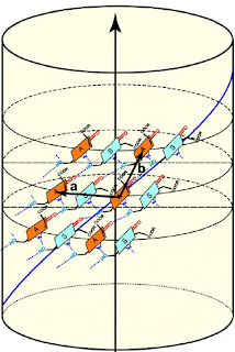
Chlorophyll Molecules and Green Bacteria

Caption: The Nuclear Magnetic Resonance (NMR) results enabled the scientists to determine that the chlorophyll molecules (shown in green and orange) in green bacteria are arranged in helical spirals, and are positioned at an angle to the long axis of the nanotubes.

Credit: Image by Donald Bryant, Penn State University, courtesy of Proceedings of the National Academy of Sciences. Usage Restrictions: The credit line -- Image by Donald Bryant, Penn State University, courtesy of Proceedings of the National Academy of Sciences-- must be published along with the picture.

Yellowstone National Park

Caption: The image shows a hot spring in Yellowstone National Park, Montana, a site where bacteria containing chlorosomes can be found in the brightly colored mats. At the upper left is a thin-section electron micrograph of the green sulfur bacterium Chlorobaculum tepidum, showing chlorosomes along the periphery of the cells as light-colored ovals. The next image is an electron micrograph of an isolated chlorosome from the bchQRU mutant, and the next image is a cryo-electron micrograph of the same. Finally, the last panel at the right shows a molecular model of the chlorophylls in the chlorosome. Individual chlorophyll molecules are illustrated in green and show their hydrophobic tails pointing outward.

Credit: Image by Donald Bryant, Penn State University, courtesy of Proceedings of the National Academy of Sciences. Usage Restrictions: The credit line -- Image by Donald Bryant, Penn State University, courtesy of Proceedings of the National Academy of Sciences -- must be published along with the picture.
Because they have been so difficult to study, the chlorosomes in green bacteria are the last class of light-harvesting complexes to be characterized structurally by scientists. Scientists typically characterize molecular structures using X-ray crystallography, a technique that determines the arrangement of atoms in a molecule and ultimately gives information that can be used to create a picture of the molecule; however, X-ray crystallography could not be used to characterize the chlorosomes in green bacteria because the technique only works for molecules that are uniform in size, shape, and structure. "Each chlorosome in a green bacterium has a unique organization," said Bryant. "They are like little andouille sausages. When you take cross-sections of andouille sausages, you see different patterns of meat and fat; no two sausages are alike in size or content, although there is some structure inside, nevertheless. Chlorosomes in green bacteria are like andouille sausages, and the variability in their compositions had prevented scientists from using X-ray crystallography to characterize the internal structure."

To get around this problem, the team used a combination of techniques to study the chlorosome. They used genetic techniques to create a mutant bacterium with a more regular internal structure, cryo-electron microscopy to identify the larger distance constraints for the chlorosome, solid-state nuclear magnetic resonance (NMR) spectroscopy to determine the structure of the chlorosome's component chlorophyll molecules, and modeling to bring together all of the pieces and create a final picture of the chlorosome.

First, the team created a mutant bacterium in order to determine why the chlorophyll molecules in green bacteria became increasingly complex over evolutionary time. To create the mutant, they inactivated three genes that green bacteria acquired late in their evolution. The team suspected that the genes were responsible for improving the bacteria's light-harvesting capabilities. "Essentially, we went backward in evolutionary time to an intermediate state in order to understand, in part, why green bacteria acquired these genes," Bryant said. The team found that the more evolved, wild-type bacteria grow faster at all light intensities than the mutant form. "Indeed, the reason that chlorophylls became more complex was to increase light-harvesting efficiency," said Bryant.

Next, the team isolated chlorosomes from the mutant and the wild-type forms of the bacteria and used cryo-electron microscopy -- a type of electron microscopy that is performed at super-cold cryogenic temperatures -- to take pictures of the chlorosomes. The pictures revealed that chlorophyll molecules inside chlorosomes have a nanotube shape. "They are like Russian dolls, with one concentric tube fitting inside the next," said Bryant. "The mutant bacterium's chlorosomes contain only one set of tubes, whereas the wild-type chlorosomes contain many tubes, each arranged in a unique pattern, like those andouille sausages."

The team then went a step further and used solid-state NMR spectroscopy -- a technique in which samples are spun very rapidly and exposed to a magnetic field -- to look deep inside the chlorosome. This technique enables researchers to understand the relationships between atomic nuclei in a sample and, ultimately, to acquire structural information about the molecules of interest.

"The NMR data revealed to us that the individual chlorophyll molecules in green bacteria are arranged in dimers -- molecules consisting of two identical simpler molecules -- with their long hydrophobic, or water-repellent, tails sticking out of either side," said Bryant. "We also learned precisely how the chlorophyll molecules attach to one another, and we were able to measure the distance between chlorophyll molecules. The cryo-electron microscopy pictures showed gross structural details and distances, and the NMR results allowed us to quantify these distances as well, and confirmed to us that what were were seeing was, in fact, stacks of the chlorophyll molecules all lined up," he said.
The NMR results also enabled the scientists to determine that the chlorophyll molecules in green bacteria are arranged in helical spirals. In the mutant bacteria, the chlorophyll molecules are positioned at a nearly 90-degree angle in relation to the long axis of the nanotubes, whereas the angle is less steep in the wild-type organism. "It's the orientation of the chlorophyll molecules that is the most important thing here," said Bryant. The last steps for the team were to pull together all of their data and to create a detailed computer model of the structure.

"At first it seems counterintuitive that green bacteria have managed to evolve a better light-harvesting system by increasing disorder in the chlorosome structure," said Bryant. "Most people would think that if you make something that is more highly ordered, you'll end up with something that works better. But this is clearly a case where that isn't true. If all of the chlorophylls are identically arranged in a chlorosome, then the energy from the photon, once it is absorbed, is going to wander around over all of those chlorophylls, which could take a long time. In the wild-type form, you have these different domains where chlorophyll molecules are located and, therefore, the ability of photon energy to migrate becomes restricted. In other words, the energy in an individual photon visits a smaller number of chlorophylls, and that's an advantage to the organism because the energy can get to where it needs to go faster. Speed is the name of the game that green bacteria play with light. The organisms have only a couple of nanoseconds for the energy to get someplace useful or else the energy is going to be lost. The speed required can be a problem for bacteria that receive only a few photons of light per chlorophyll per day."

Bryant said that the team's results may one day be used to build artificial photosynthetic systems that convert solar energy to electricity. "The interactions that lead to the assembly of the chlorophylls in chlorosomes are rather simple, so they are good models for artificial systems," he said. "You can make structures out of these chlorophylls in solution just by having the right solution conditions. In fact, people have done this for many years; however, they haven't really understood the biological rules for building larger structures. I won't say that we completely understand the rules yet, but at least we know what two of the structures are now and how they relate to the biological system as a whole, which is a huge advance." ###

The team also includes researchers from the Leiden Institute of Chemistry and the Groningen Biomolecular Sciences and Biotechnology Institute in the Netherlands, and the Max Planck Institute in Germany. This research was supported by the United States Department of Energy.

CONTACTS:
Donald Bryant: (+1) 814-865-1992, dab14@psu.edu
Barbara Kennedy (PIO): (+1) 814-863-4682, science@psu.edu

Contact: Barbara K. Kennedy science@psu.edu 814-863-4682 Penn State