Saturday, May 30, 2009

UConn chemists find secret to increasing luminescence efficiency of carbon nanotubes VIDEO

STORRS, Conn. - Chemists at the University of Connecticut have found a way to greatly increase the luminescence efficiency of single-walled carbon nanotubes, a discovery that could have significant applications in medical imaging and other areas.

Increasing the luminescence efficiency of carbon nanotubes may someday make it possible for doctors to inject patients with microscopic nanotubes to detect tumors, arterial blockages and other internal problems. Rather than relying on potentially harmful x-rays or the use of radioactive dyes, physicians could simply scan patients with an infrared light that would capture a very sharp resolution of the luminescence of the nanotubes in problem areas.

Fotios Papadimitrakopoulos

Fotios Papadimitrakopoulos: SINGLE WALL CARBON NANOTUBES (SWNTs) VIDEO: The wrapping of SWNTs with a seamless, conformal helix made out of small molecular weight material has been a major challenge in the field of SWNTs.
UConn's process of increasing the luminescence efficiency of single-walled carbon nanotubes will be featured in Science magazine on Friday, March 6, 2009. The research was performed in the Nanomaterials Optoelectronics Laboratory at the Institute of Materials Science at the University of Connecticut, in Storrs, CT. A patent for the process is pending.

University of Connecticut Chemist Fotios Papadimitrakopoulos describes the discovery as a major breakthrough and one of the most significant discoveries in his 10 years of working with single-walled carbon nanotubes. Assisting Papadimitrakopoulos with the research were Polymer Program graduate student Sang-Yong Ju (now a researcher at Cornell University) and William P. Kopcha, a former Chemistry undergraduate assistant in the College of Liberal Arts and Sciences who is now a first-year graduate student at UConn.
Although carbon is used in many diverse applications, scientists have long been stymied by the element's limited ability to emit light. The best scientists have been able to do with solution-suspended carbon nanotubes was to raise their luminescence efficiency to about one-half of one percent, which is extremely low compared to other materials, such as quantum dots and quantum rods.

By tightly wrapping a chemical 'sleeve' around a single-walled carbon nanotube, Papadimitrakopoulos and his research team were able to reduce exterior defects caused by chemically absorbed oxygen molecules.

This process can best be explained by imagining sliding a small tube into a slightly larger diameter tube, Papadimitrakopoulos says. In order for this to happen, all deposits or protrusions on the smaller tube have to be removed before the tube is allowed to slip into the slightly larger diameter tube. What is most fascinating with carbon nanotubes however, Papadimitrakopoulos says, is the fact that in this case the larger tube is not as rigid as the first tube (i.e. carbon nanotube) but is rather formed by a chemical "sleeve" comprised of a synthetic derivative of flavin (an analog of vitamin B2) that adsorbs and self organizes onto a conformal tube.

Papadimitrakopoulos claims that this process of self-assembly is unique in that it not only forms a new structure but also actively "cleans" the surface of the underlying nanotube. It is that active cleaning of the nanotube surface that allows the nanotube to achieve luminescence efficiency to as high as 20 percent.

The nanotube is the smallest tube on earth and we have found a sleeve to put over it," Papadimitrakopoulos says. "This is the first time that a nanotube was found to emit with as much as 20 percent luminescence efficiency."

Papadimitrakopoulos has been working closely with the UConn Center for Science and Technology Commercialization (CSTC) in transferring his advances in research into the realm of patents, licenses and corporate partnerships. The CSTC was created several years ago as a way to help expand Connecticut's innovation-based economy and to help create new businesses and jobs around new ideas.

This is the second major nanotube discovery at UConn by Papadimitrakopoulos in the past two years. Last year, Papadimitrakopoulos and Sang-Young Ju, along with other UConn researchers, patented a way to isolate certain carbon nanotubes from others by seamlessly wrapping a form of vitamin B2 around the nanotubes. It was out of that research that Papadimitrakopoulos and Sang-Yong Ju began wrapping nanotubes with helical assemblies and probing their luminescence properties.

The more luminescent the nanotube, the brighter it appears under infrared irradiation or by electrical excitation (such as that provided by a light-emitting diode or LED). A number of important applications may be possible as a result of this research, Papadimitrakopoulos says. Carbon nanotube emissions are not only extremely sharp, but they also appear in a spectral region where minimal absorption or scattering takes place by soft tissue. Moreover, carbon nanotubes display superb photo bleaching stability and are ideally suited for near-infrared emitters, making them appropriate for applications in medicine and homeland security as bio-reporting agents and nano-sized beacons. Carbon nanotube luminescence also has important applications in nano-scaled LEDs and photo detectors, which can readily integrate with silicon-based technology. This provides an enormous repertoire for nanotube use in advanced fiber optics components, infrared light modulators, and biological sensors, where multiple applications are possible due to the nanotube's flavin-based (vitamin B2) helical wrapping. ###

Additional Contact Information: Fotios Papadimitrakopoulos Professor of Chemistry Associate Director, Institute of Materials Science University of Connecticut Tel: (860)-486-3447, Fax: (860)-486-4745, Email: papadim@mail.ims.uconn.edu

More information about the University of Connecticut's Nanomaterials Optoelectronics Laboratory can be found at: chemistry.uconn.edu/papadim/

Contact: Colin Poitras colin.poitras@uconn.edu 860-486-4656 University of Connecticut

Thursday, May 28, 2009

Buckyballs could keep water systems flowing

DURHAM, N.C. – Microscopic particles of carbon known as buckyballs may be able to keep the nation's water pipes clear in the same way clot-busting drugs prevent arteries from clogging up.

Engineers at Duke University have found that buckyballs hinder the ability of bacteria and other microorganisms to accumulate on the membranes used to filter water in treatment plants. This attribute leads the researchers to believe that coating pipes and membranes with these nanoparticles may prove to be an effective strategy for addressing one of the major problems and costs of treating water.

"Just as plaque can build up inside arteries and reduce the flow of blood, bacteria and other microorganisms can over time attach and accumulate on water treatment membranes and along water pipes," said So-Ryong Chae, post-doctoral fellow in Duke's environmental and civil engineering department. The results of his experiments were published March 5, 2009 in the Journal of Membrane Sciences.

Buckyball-Treated Membrane

Caption: This is a buckyball-treated membrane. Credit: Duke University. Usage Restrictions: None.
"As the bacteria build up on these surfaces, they attract other organic matter, creating a biofilm that slowly builds up over time," Chae continued, "The results of our experiments in the laboratory indicate that buckyballs may be able to prevent this clogging, known as biofouling. The only other options to address biofouling are digging up the pipes and replacing the membranes, which can be expensive and inconvenient."
A buckyball, or C60, is one shape within the family of tiny carbon shapes known as fullerenes. They are named after Richard Buckminster Fuller, the inventor of the geodesic dome, since their shape resembles his famous structure.
"Biofouling is viewed as one of the biggest costs associated with membrane-based water treatment systems," said Claudia Gunsch, assistant professor of civil engineering at Duke's Pratt School of Engineering and senior member of the research team. "These membranes have very small pores, so they can get stopped up quickly. If we could increase the time between membrane replacements by 50 percent, for example, that would be a huge cost savings."Membrane Without Buckyball Treatment

Caption: This is a membrane without buckyball treatment. Credit: Duke University. Usage Restrictions: None.
According to Chae, the addition of buckyballs to treatment membranes had a two-fold effect. First, treated membranes showed less bacterial attachment than non-treated membranes. After three days, the membranes treated with buckyballs had on average 20 colony forming units, the method by which bacterial colonies are counted.

"In contrast, the number of bacterial colonies on the untreated membrane was too numerous to count," Chae said.

Chae also found that the presence of the buckyballs inhibited respiration, or the ability of the bacteria to use oxygen to fuel its activities.

"As the concentration of buckyballs increased, so did the inhibition of respiration," Chae said. "This respiratory inhibition and anti-attachment suggests that this nanoparticle may be useful as an anti-fouling agent to prevent the biofouling of membranes or other surfaces."

Gunsch said the mechanisms involved are not well-understood.

Both Gunsch and Chae believe that since buckyballs are one of the most widely used nanoparticles, additional research is needed to determine if they have any detrimental effects on the environment or to humans. This is one of many issues being studied at Duke's Center for Environmental Implications of Nanotechnology.

"We need to figure out how resistant these coatings will be to long-term use," Gunsch said. "If they can indeed prevent fouling, they will last longer. If they slough off over time, we need to know what the effects will be."

The current experiments in the laboratory were conducted with Escherichia coli K12, a strain of the bacteria that is widely used in laboratory experiments.

"We focused on a quite specific microorganism, so the next stage of our research will to see if these nanoparticles will have the same effects on bacteria commonly found in the environment or those in mixed microbial communities," Chae said. "We also plan to build a small-scale version of a treatment plant in the lab to conduct these tests." ###

The research was supported by the Office of Naval Research, National Science Foundation and the Korea Research Foundation. Other Duke members of the team were Shuyi Wang, Zachary Hendren and Mark R. Wiesner. Yoshimasa Watanabe, Hokkaido University, Japan, was also part of the team.

Contact: Richard Merritt richard.merritt@duke.edu 919-660-8414 Duke University

Tuesday, May 26, 2009

'Nanostitching' could lead to much stronger airplane skins, more

MIT engineers are using carbon nanotubes only billionths of a meter thick to stitch together aerospace materials in work that could make airplane skins and other products some 10 times stronger at a nominal increase in cost.

Moreover, advanced composites reinforced with nanotubes are also more than one million times more electrically conductive than their counterparts without nanotubes, meaning aircraft built with such materials would have greater protection against damage from lightning, said Brian L. Wardle, the Charles Stark Draper Assistant Professor in the Department of Aeronautics and Astronautics.

Wardle is lead author of a theoretical paper on the new nanotube-reinforced composites that will appear in the Journal of Composite Materials (http://jcm.sagepub.com). He also described the work as keynote speaker at a Society of Plastics Engineers conference this week.

Brian Wardle MIT

Brian Wardle, the Charles Stark Draper Assistant Professor in the Department of Aeronautics and Astronautics, shows an advanced composite material held together by "nanostitching," a technique developed at MIT that could make airplane skins and other products stronger. Photo / Donna Coveney
The advanced materials currently used for many aerospace applications are composed of layers, or plies, of carbon fibers that in turn are held together with a polymer glue. But that glue can crack and otherwise result in the carbon-fiber plies coming apart. As a result, engineers have explored a variety of ways to reinforce the interface between the layers by stitching, braiding, weaving or pinning them together.
All of these processes, however, are problematic because the relatively large stitches or pins penetrate and damage the carbon-fiber plies themselves. "And those fiber plies are what make composites so strong," Wardle said.
So Wardle wondered whether it would make sense to reinforce the plies in advanced composites with nanotubes aligned perpendicular to the carbon-fiber plies. Using computer models of how such a material would fracture, "we convinced ourselves that reinforcing with nanotubes should work far better than all other approaches," Wardle said. His team went on to develop processing techniques for creating the nanotubes and for incorporating them into existing aerospace composites, work that was published last year in two separate journals.carbon nanotubes

Schematic showing carbon nanotubes bridging the gap between plies of an advanced composite. Graphic courtesy / Wardle lab, MIT
How does nanostitching work? The polymer glue between two carbon-fiber layers is heated, becoming more liquid-like. Billions of nanotubes positioned perpendicular to each carbon-fiber layer are then sucked up into the glue on both sides of each layer. Because the nanotubes are 1000 times smaller than the carbon fibers, they don't detrimentally affect the much larger carbon fibers, but instead fill the spaces around them, stitching the layers together.

"So we're putting the strongest fibers known to humankind [the nanotubes] in the place where the composite is weakest, and where they're needed most," Wardle said. He noted that these dramatic improvements can be achieved with nanotubes comprising less than one percent of the mass of the overall composite. In addition, he said, the nanotubes should add only a few percent to the cost of the composite, "while providing substantial improvements in bulk multifunctional properties."

Wardle's co-authors on the Journal of Composite Materials paper are Joaquin Blanco, a visiting graduate student in the Department of Aeronautics and Astronautics, Enrique J. Garcia SM '06, and Roberto Guzman deVilloria, a postdoctoral associate in the department.

This research was sponsored by MIT's Nano-Engineered Composite aerospace STructures (NECST) Consortium (necst.mit.edu).

Elizabeth A. Thomson, News Office Contact: Elizabeth Thomson thomson@mit.edu 617-258-5402 Massachusetts Institute of Technology

Monday, May 25, 2009

Researchers discover a potential on-off switch for nanoelectronics

Berkeley, CA - As electronic circuits shrink from finely etched lines in silicon wafers to nearly elusive proportions, researchers at the U.S. Department of Energy's Lawrence Berkeley National Laboratory (Berkeley Lab) and Columbia University are studying how electrons flow through a molecular junction—a nanometer scale circuit element that contacts gold atoms with a single molecule. Their findings reveal the electrical resistance through this junction can be turned 'on' and 'off' simply by pushing and pulling the junction—a feature that could be used as a switch in nanoscale electronic devices.

"To design circuit elements at the molecular scale, we need to understand how the intrinsic properties of a molecule or junction are actually connected to its measured resistance," said Jeff Neaton, Facility Director of the Theory of Nanostructured Materials Facility in the Molecular Foundry, a U.S. Department of Energy User Facility located at Berkeley Lab that provides support to nanoscience researchers around the world.

Molecular Junctions

Caption: These schematics illustrate the "vertical" and "angled" molecular junction configurations for mechanically-induced switching. A study has revealed that electrical resistance through such a junction can be turned "on" and "off" simply by pushing (left) so that the configuration is vertical or and by pulling the junction so that the configuration is angled.

Credit: The Molecular Foundry, Lawrence Berkeley National Laboratory. Usage Restrictions: None.
"Knowing where each and every atom is in a single-molecule junction is simply beyond what's possible with experiments at this stage. For these sub-nanometer scale junctions—just a handful of atoms—theory can be valuable in helping interpret and understand resistance measurements."

In traditional electronic devices, charge-carrying electrons diffuse through circuits in a well-understood fashion, gaining or losing energy through transactions with impurities or other particles they encounter. Electrons at the nanoscale, however, can travel by a mechanism called quantum tunneling in which, due to the small length scales involved, it becomes possible for a particle to disappear through an energy barrier and suddenly appear on the other side, without expending energy. Tracking such 'tunneling' of electrons through individual molecules in nanoscale devices has proven difficult.
"For more than a decade, researchers have been 'wiring up' individual molecules and measuring their electrical conductance," said Neaton. "Forming reliable contacts between nanostructures and 'alligator clip' electrical leads is extremely challenging. This made experiments difficult to interpret, and as a result, reported conductance values—in experiment and theory—often varied by an order of magnitude or more. The time was ripe for a quantitative comparison between theory and an experiment with well-defined contacts."
Through the Molecular Foundry user program, Su Ying Quek, a postdoctoral researcher, worked with Neaton and Latha Venkataraman, an experimental researcher at Columbia University, using a scanning tunneling microscope (STM), which probes changes in current across a material's surface with a conductive gold tip. Previous work had shown a gold STM tip could be repeatedly be plunged into a gold surface containing a solution of molecules and retracted, until the contact area between the tip and gold surface reduces to a single strand,Jeff Neaton, DOE/Lawrence Berkeley National Laboratory

Caption: Jeffrey Neaton is director of the Theory of Nanostructured Materials facility at The Molecular Foundry.

Credit: Roy Kaltschmidt, Berkeley Lab Public Affairs. Usage Restrictions: None.
like a necklace. When this strand finally breaks, nearby molecules can hop into the gap between strands and contact the gold electrodes, resulting in a sudden change in conductance. Using this technique, Venkataraman and colleagues, including Mark Hybertsen at Brookhaven National Lab, had recently discovered that the conductance of molecules containing amines (a group of molecules related to ammonia) in contact with gold electrodes could be reliably measured.

"We now had a reproducible and consistent data set to benchmark our theory," said Quek. "Comparing with this data set, we discovered important electron correlation effects previously missing. When we added these, we found—for the first time—quantitative agreement with experimental results."

Using their new theoretical approach, Quek and Neaton, together with Hybertsen and collaborators Steven G. Louie of University of California Berkeley and Hyoung Joon Choi of Yonsei University in Korea, began to study the conductance of a junction between gold electrodes and bipyridine—a benzene-like ring molecule containing nitrogen. The experimental data showed two stable conductance states, unlike anything seen previously. Working closely with Venkataraman and collaborators, Quek hypothesized the peaks corresponded to two states with different structures within the junction. During the next year, Quek and Neaton meticulously constructed a theory that could describe the conductance of junctions arranged vertically between two gold molecules and sandwiched at angles.

The story that emerged was surprisingly detailed: if bipyridine bonded at an angle, more current could flow compared with when the bipyridine bonded vertically. This suggests the conductance of bipyridine was linked to the molecule's orientation in the junction, explained Quek. In the STM experiment, as you pull, just after the final strand of gold atoms breaks and snaps back, the vertical gap is not big enough for bipyridine, so it bonds at an angle. As the gap increases, the molecule jumps to a vertical configuration, causing the conductance to plummet abruptly. Eventually, the molecule straightens even more, and the contact breaks. "Once we determined this, we wondered, 'could you reverse this behavior?'" said Quek.

Teaming with Venkataraman and collaborators, Quek and Neaton demonstrated why pushing the junction to an angle and pulling it straight could repeatedly alter the conductance, creating a mechanical switch with well defined 'on' and 'off' states. "One of the fascinating things about this experiment is the degree to which it is possible to control the 'alligator clips'," said Neaton. "For this particular molecule, bipyridine, experiments can reproducibly and reliably alter these atomic-scale features back and forth to switch the conductance of the junction."

Quek and Neaton hope to refine and apply their theoretical framework to more complex molecular junctions for study of systems promising for solar energy conversion, such as organic photovoltaics.

"Understanding how electrons move through single-molecule junctions is the first step," said Neaton. "Organic-inorganic interfaces are everywhere in nanoscience, and developing a better picture of charge transport in hybrid materials systems will certainly lead to the discovery of new and improved electronic devices." ###

"Mechanically-controlled binary conductance switching of a single-molecule junction," by Su Ying Quek, Maria Kamenetska, Michael L. Steigerwald, Hyoung Joon Choi, Steven G. Louie, Mark S. Hybertsen, J.B. Neaton and L. Venkataraman, appears in Nature Nanotechnology and is available in Nature Nanotechnology online.

Portions of this work were supported by the U.S. Department of Energy (DOE) Office of Science, through its Office of Basic Energy Sciences, and by the National Science Foundation through its Nanoscale Science and Engineering Initiative.

The Molecular Foundry is one of the five DOE Nanoscale Science Research Centers (NSRCs), premier national user facilities for interdisciplinary research at the nanoscale. Together the NSRCs comprise a suite of complementary facilities that provide researchers with state-of-the-art capabilities to fabricate, process, characterize and model nanoscale materials, and constitute the largest infrastructure investment of the National Nanotechnology Initiative. The NSRCs are located at DOE's Argonne, Brookhaven, Lawrence Berkeley, Oak Ridge, and Sandia and Los Alamos National Laboratories. For more information about the DOE NSRCs, please visit nano.energy.gov.

Berkeley Lab is a U.S. Department of Energy national laboratory located in Berkeley, California. It conducts unclassified scientific research and is managed by the University of California. Visit our website at www.lbl.gov.

Contact: Aditi Risbud ASRisbud@lbl.gov 510-486-4861 DOE/Lawrence Berkeley National Laboratory

Saturday, May 23, 2009

Nanostructure boosts efficiency in energy transport

Complimentary semiconductors enhance 'water-splitting' technique

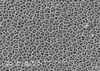
CHESTNUT HILL, MA (March 3, 2009) – Overcoming a critical conductivity challenge to clean energy technologies, Boston College researchers have developed a titanium nanostructure that provides an expanded surface area and demonstrates significantly greater efficiency in the transport of electrons.

The challenge has vexed researchers pursuing solar panels thick enough to absorb sunlight, yet thin enough to collect and transport electrons with minimal energy loss. Similarly, the relatively new science of water splitting requires capturing energy within semiconductor materials and then efficiently transporting charges ultimately used to generate hydrogen.

Microscopic View of Titanium Nanostructure

Caption: A net-like titanium nanostructure, shown here under a transmission electron micrograph, grown by Boston College chemists from a titanium disilicide core for improved conductivity and a coating of titanium dioxide, required for its catalytic prowess. The material shows promise for use in water splitting, the process of chemically separating oxygen and hydrogen gasses to produce clean energy.

Credit: Journal of the American Chemical Society. Usage Restrictions: None.
Boston College Asst. Prof of Chemistry Dunwei Wang and members of his lab found that incorporating two titanium-based semiconductors into a nano-scale structure improved the efficiency of power-collecting efforts by approximately 33 percent, the team reported in the online edition of the Journal of the American Chemical Society.

The team achieved a peak conversion efficiency of 16.7 percent under ultraviolet light, reported Wang and his co-authors, BC graduate students Yongjing Lin and Sa Zhou, post doctoral researcher Xiaohua Liu and undergraduate Stafford Sheehan. That compared to an efficiency of 12 percent from a structure composed only of titanium dioxide (TiO2).
Wang said the efficiency gains within the novel material can serve so-called water-splitting, where semiconductor catalysts have been shown to separate and store hydrogen and oxygen gases.
"The current challenge in splitting water involves how best to capture photons within the semiconductor material and then grab and transport them to produce hydrogen," Wang says. "For practical water splitting, you want to generate oxygen and hydrogen separately. For this, good electrical conductivity is of great importance because it allows you to collect electrons in the oxygen-generation region and transport them to the hydrogen-generation chamber for hydrogen production."An Improved Titanium Nanostructure

Caption: An illustration of a titanium nanostructure grown by researchers from Boston College, who report the material is capable of providing expanded surface area and improved conductivity, two qualities seen as critical in the search for clean energy technologies.

Credit: Journal of the American Chemical Society. Usage Restrictions: None.
By using two crystalline semiconductors – materials critical to the processes of energy capture and transport – Wang says the researchers discovered a new and successful transfer mechanism in an engineered structure nearly invisible to the human eye.

Titanium dioxide has played a key role in early water-splitting research because of its prowess as a catalyst. However, its light absorption is confined to ultraviolet rays only and the material is also a relatively poor conductor.

Wang and his researchers started by growing a nanostructure made of titanium disilicide (TiSi2), a semiconductor capable of absorbing solar light and a material able to provide a sturdy structure with expanded surface area critical to absorbing photons. Still in need of its catalytic capabilities, titanium dioxide was used to coat the structure, Wang said.

The resulting net-like nanostructure effectively separated charges, collecting the electrons in the titanium disilicide core and transporting them away. The structure transferred positive charges to the titanium dioxide region of the material for chemical reactions. In water-splitting, these charges could potentially be used to generate hydrogen. ###

The paper can be viewed online at the Journal of the American Chemical website at pubs.acs.org/doi/abs/10.1021/. For more information about Prof. Wang's lab, please visit the website: www2.bc.edu/~dwang/.

Contact: Ed Hayward ed.hayward@bc.edu 617-552-4826 Boston College

Thursday, May 21, 2009

Models present new view of nanoscale friction

To understand friction on a very small scale, a team of UW-Madison engineers had to think big.

Friction is a force that affects any application where moving parts come into contact; the more surface contact there is, the stronger the force. At the nanoscale — mere billionths of a meter — friction can wreak havoc on tiny devices made from only a small number of atoms or molecules. With their high surface-to-volume ratio, nanomaterials are especially susceptible to the forces of friction.

But researchers have trouble describing friction at such small scales because existing theories are not consistent with how nanomaterials actually behave. Through computer simulations, the group demonstrated that friction at the atomic level behaves similarly to friction generated between large objects. Five hundred years after Leonardo da Vinci discovered the basic friction laws for large objects, the UW-Madison team has shown that similar laws apply at the nanoscale.

nanoscale interface between carbon and diamond

This graphic recreates an atom-level view of the nanoscale interface between carbon and diamond. At such a small scale, the surfaces are rough, although researchers have been treating them as smooth. Image: Izabela Szlufarska

The team, which was led by Izabela Szlufarska, an assistant professor of materials science and engineering, and included materials science and engineering graduate student Yifei Mo and mechanical engineering assistant professor Kevin Turner, published its findings in the Feb. 26 issue of the journal Nature.

Current nanoscale friction theories are based on the idea that nanoscale surfaces are smooth, but, in reality, the surfaces resemble a mountain range, where each peak corresponds to an atom or a molecule.

The UW-Madison team performed computer simulations that looked at nanoscale materials as a collection of atoms, monitoring their positions and interactions throughout the entire sliding process. "For the first time, we modeled friction at length scales very similar to experiments, while maintaining atomic resolution and realistic interactions between atoms," say Szlufarska.

The team discovered simple laws of nanoscale friction. They found that friction is proportional to the number of atoms that interact between two nanoscale surfaces. The researchers' simulations showed that, at the nanoscale, materials in contact behave more like large rough objects rubbing against each other, rather than as two perfectly smooth surfaces, as was previously imagined. "When you look at it closely, the surface is made of atoms, so the contact is actually rough," says Szlufarska.

The team's simulation data correlates very well with recorded experimental data — something that previous models have failed to accomplish. Szlufarska hopes to use the simulations as a tool to understand what mechanisms contribute to friction on both the nano- and macroscale.

"Nobody is able to predict friction or design materials with desired friction properties — we measure a lot of friction coefficients for different materials, but it's not really clear how to relate them to the properties of the material," she explains. "The origin of friction is really an open and growing research field."

The National Science Foundation and by the American Chemical Society Petroleum Research Fund supported the team's research.

by Liz Ahlberg Contact: Izabela Szlufarska izabela@engr.wisc.edu WEB: University of Wisconsin-Madison

Tuesday, May 19, 2009

Team develops new metamaterial device

Solid-state metamaterial device tames terahertz frequency

CHESTNUT HILL, MA (February 24, 2009) – An engineered metamaterial proved it can function as a state-of-the-art device in the complex terahertz range of the electromagnetic spectrum, setting a standard of performance for modulating tiny waves of radiation, according to a team of researchers from Boston College, the Los Alamos and Sandia national laboratories, and Boston University.

An electrical current applied to the metamaterial – a hybrid structure of metallic split-ring resonators – controlled the phase of a terahertz (THz) beam 30 times faster and with far greater precision than a conventional optical device, the researchers report in the current online edition of the journal Nature Photonics.

Dr. Willie J. Padilla

Dr. Willie J. Padilla
The discovery marks a milestone in the use of metamaterials and terahertz radiation, a safe, non-ionizing frequency that is the subject of a growing body of research and viewed as a promising component in applications that include advanced security screening systems and imaging technologies.
"This is a true metamaterial device," Boston College Asst. Prof. of Physics Willie J. Padilla, one of the co-authors of the paper, said. "This highlights the fact that you can make solid state devices at terahertz frequencies with metamaterials."

Constructed on the micron-scale, metamaterials are composites that use unique metallic contours in order to produce responses to light waves, giving each metamaterial its own unique properties beyond the elements of the actual materials in use. Within the past decade, researchers have sought ways to significantly expand the range of material responses to waves of electromagnetic radiation – classified by increasing frequency as radio waves, microwaves, terahertz radiation, infrared radiation, visible light, ultraviolet radiation, X-rays and gamma rays. These metamaterials have demonstrated numerous novel effects that defy accepted electromagnetic principles.

Previously, in systems known as THz time domain spectrometers, the flow of terahertz radiation has been modulated indirectly by optical choppers, mechanical devices that either blocked a laser or allowed it to pass through. This "all or nothing" approach – similar to opening and closing the shutter of a camera – limits the speed with which one can manipulate terahertz waves since the chopper's mechanical components are too slow, Padilla says.

The metamaterial devised by the research team electronically controlled the flow of terahertz radiation over roughly 70 percent of the frequency band – not simply at the points of maximum or minimum frequency.

"We can apply an electronic signal to this device, thus making it opaque to stop terahertz, or transparent to allow terahertz through," Padilla said. "Eventually, you can turn it on and off very quickly – and that allows you to modulate the beam at a very specific frequency."

Because the metamaterial device is solid-state, eliminating moving parts, it is 30 times faster than the optical chopper, according to the report, co-authored by Hou-Tong Chen, Abul K. Azad and Antoinette J. Taylor of Los Alamos National Laboratory, Michael J. Cich of Sandia National Laboratories and Richard D. Averitt of Boston University

"The advantage of the metamaterial is you are doing it electronically," Padilla said. "If you want to build a device, the advantage of this is that it is all solid-state and voltage controlled. You have no moving parts. Therefore, you can modulate at very high speeds."

These kinds of controls have been developed for microwave and optical frequencies and led to a number of key breakthroughs, the researchers note. But the technologies have not extended to the terahertz frequency.

Padilla said a solid-state metamaterial device is a critical step toward improved terahertz devices, such as cameras or scanners.

"What we've shown with this metamaterial is that it is now improved to the point where it could be used as a device," Padilla said. "It could be the device you could use to build a terahertz system." ###

The research is supported by the Laboratory Directed Research and Development program at Los Alamos National Laboratory.

To learn more about Prof. Padilla's lab, please see: www2.bc.edu/~padillaw/

Contact: Ed Hayward ed.hayward@bc.edu 617-552-4826 Boston College

Sunday, May 17, 2009

Case Western Reserve researchers develop 'wireless' activation of brain circuits

Burda and Strowbridge offer firsrt report of brain stimulation using light-activated semiconductor nanoparticles

Traditionally, stimulating nerves or brain tissue involves cumbersome wiring and a sharp metal electrode. But a team of researchers at Case Western Reserve University is going "wireless."

And it's a unique collaboration between chemists and neuroscientists that led to the discovery of a remarkable new way to use light to activate brain circuits with nanoparticles.

Ben Strowbridge, an associate professor in the neurosciences department in the Case Western Reserve School of Medicine and Clemens Burda, an associate professor in chemistry, say it's rare in science that people from very different fields get together and do something that is both useful and that no one had thought of before. But that is exactly what they've done.

Ben W. Strowbridge, Ph.D.

Ben W. Strowbridge, Ph.D. Associate Professor of Neuroscience
By using semiconductor nanoparticles as tiny solar cells, the scientists can excite neurons in single cells or groups of cells with infrared light. This eliminates the need for the complex wiring by embedding the light-activated nanoparticles directly into the tissue. This method allows for a more controlled reaction and closely replicates the sophisticated focal patterns created by natural stimuli.
The electrodes used in previous nerve stimulations don't accurately recreate spatial patterns created by the stimuli and also have potential damaging side effects.

"There are many different things you'd want to stimulate neurons for-injury, severed or damaged nerve to restore function- and right now you have to put a wire in there, and then connect that to some control system. It is both very invasive and a difficult thing to do," says Strowbridge.

IIn principle, the researchers should be able to implant these nanoparticles next to the nerve, eliminating the requirement for wired connections. They can then use light to activate the particles.

"We believe it has a lot of applicability," they said" Hopefully, the same thing can happen in the brain."

The researchers' paper, "Wireless Activation of Neurons in Brain Slices Using Nanostructured Semiconductor Photoelectrodes," is the first report of brain stimulation using light-activated semiconductor nanoparticles. This research study was published in Angewandte Chemie, a premier chemistry journal. The journal also highlighted the study as a "hot paper."

This study used brain slices to show that light can trigger neural activity. The next step is to see if this innovative technology can be used to stimulate longer pathways within the intact brain. Clinical development of the technology could lead to new methods to activate specific brain regions and damaged nerves.

"The long-term goal of this work is to develop a light-activated brain-machine interface that restores function following nerve or brain impairments," Strowbridge says. "The first attempts to interface computers with brain circuitry are being done now with complex metal electrode stimulation arrays that are not well suited to recreating normal brain activity patterns and also can cause significant damage."

Currently light is being used in the study to drive neural activity in a minimally invasive manner, without requiring electrical wires.

The pair credits Pamela Davis, dean of the School of Medicine, for introducing them several years ago. "It is great to have a medical school dean who knows not only what her own faculty are doing but also closely follows the research programs in other colleges," says Strowbridge. Campus geography played a role as well. "This project would not have happened without the close physical proximity between the two departments," says Burda. "Case Western Reserve is unusual in having its medical school located on the same campus as the rest of the University."

When they aren't brought together for this collaboration, the two labs pursue vastly different research programs. Strowbridge's laboratory is interested in how groups of neurons are wired together in both the brain regions responsible for the sense of smell and in the hippocampus, a critical brain area for both memory and epilepsy.

Burda's laboratory uses chemically synthesized nanostructures to study renewable energy conversion schemes, including solar cells. He also investigates nanoparticles for targeted drug delivery and therapy.

"It took a lot of extra hours above and beyond their regular projects for our students to complete this project," Burda says. "Fortunately, we have great students who were really excited about the potential applications of this technology from the beginning and found ways to make this project work,"

Phillip Larimer and Todd Pressler, from Strowbridge's group, and Yixin Zhao, from Burda's team, worked on the project outside of their primary lab responsibilities, conducting tests and recording data, creating software and measuring their results. The three graduate students are co-authors on the paper with the two researchers.

"Our findings may open up a whole new world of research possibilities Now all we have to do is get real funding for this project to take it to the next level," Burda says.

The researchers point out that it is often challenging to get federal funding for this type of interdisciplinary research. Traditional grant review panels are specialized to review either chemistry or neuroscience proposals, but not proposals at the interface between the two disciplines.

Fortunately, both laboratories are established and well funded for their primary research programs. "We were able to jumpstart this project using our existing grant support because of the potential impact this work may have for our long-term research programs," says Strowbridge. ###

Contact: Jason A. Tirotta jason.tirotta@case.edu 216-368-6890 Case Western Reserve University

Saturday, May 16, 2009

Safer nanoparticles spotlight tumors, deliver drugs

Small is promising when it comes to illuminating tiny tumors or precisely delivering drugs, but many worry about the safety of nano-scale materials. Now a team of scientists has created miniscule flakes of silicon that glow brightly, last long enough to slowly release cancer drugs, then break down into harmless by-products.

"It is the first luminescent nanoparticle that was purposely designed to minimize toxic side effects," said Michael Sailor, a chemistry professor at the University of California, San Diego who led the study.

Many nanoparticles tested in research labs are too poisonous for use in humans.

"This new design meets a growing need for non-toxic alternatives that have a chance to make it into the clinic to treat human patients," Sailor said.

Glowing Nanoparticles

Caption: Silicon nanoparticles are engineered to glow red under ultraviolet light. Credit: Luo Gu. Usage Restrictions: To illustrate articles about this research only.

silicon nanoparticles

Caption: New silicon nanoparticles illuminate tissues without harm. Credit: Luo Gu. Usage Restrictions: To illustrate articles about this research only.

Silicon Nanoparticles

Caption: This is a microscopic view of silicon flakes designed to deliver drugs, then dissolve away. Credit: Luo Gu. Usage Restrictions: To illustrate articles about this research only.
The particles inherently glow, a useful property that is most commonly achieved by including toxic organic chemicals or tiny structures called quantum dots, which can leave potentially harmful heavy metals in their wake.

When the researchers tested their safer nanoparticles in mice, they saw tumors glow for several hours, then dim as the particles broke down. Levels dropped noticeably in a week and were undetectable after four weeks, they report in Nature Materials February 22.

This is the first sudy to image tumors and organs using biodegradable silicon nanoparticles in live animals, the authors say.

The particles begin as thin wafers made porous with an electrical current then smashed to bits with ultrasound. Additional treatment alters the physical structure of the flakes to make them glow red when illuminated with ultraviolet light.

Luminescent particles can reveal tumors too tiny to detect by other means or allow a surgeon to be sure all of a cancerous growth has been removed.

These nanoparticles could also help deliver drugs safely, the researchers report. The cancer drug doxorubicin will stick to the pores and slowly escape as the silicon dissolves.

"The goal is to use the nanoparticles to chaperone the drug directly to the tumor, to release it into the tumor rather than other parts of the body," Sailor said.

Targeted delivery would allow doctors to use smaller doses of the drug. At doses high enough to be effective, when delivered to the whole body, doxorubicin often has toxic side effects.

At about 100 nanometers, these particles are bigger than many designed to deliver drugs, which can be just a few nanometers across – a thousand times smaller than the diameter of a human hair.

Their larger size contributes to both their effectiveness and their safety. Large particles can hold more of a drug. Yet they self-destruct, and the remnants can be filtered away by the kidneys.
Close examination of vulnerable organs like liver, spleen and kidney, which help to remove toxins, revealed no lasting changes in mice treated with the new nanoparticles. ###

Graduate students Ji-Ho Park and Luo Gu in Sailor's lab; Sangeeta Bhatia, bioengineering professor at the Massachusetts Institute of Technology and graduate student Geoffrey von Malzahn in Bhatia's lab; and Erkki Ruoslahti, professor at the University of California, Santa Barbara all contributed to this work.

The National Cancer Institute and the National Science Foundation funded this research.

Media Contact: Susan Brown 858-246-0161 sdbrown@ucsd.edu Contact: Michael Sailor msailor@ucsd.edu WEB: University of California - San Diego

Thursday, May 14, 2009

Gold-palladium nanoparticles achieve greener, smarter production of hydrogen peroxide

Processing in smaller quantities and more useful concentrations is seen

Hydrogen peroxide is one of the world's most versatile and widely used chemicals. A powerful oxidizing agent, H2O2 is commonly used as a bleach, an antiseptic and a disinfectant.

Despite its importance, however, says Christopher J. Kiely, hydrogen peroxide has eluded the best efforts of the chemists seeking a more direct, efficient and environmentally friendly means of producing it.

"Hydrogen peroxide has for decades been made by an indirect energy-intensive process," says Kiely, a professor of materials science and engineering at Lehigh University.

Christopher J. Kiely

Christopher J. Kiely
There are other disadvantages, Kiely adds. The economics of the current production method requires H2O2 to be produced in large quantities and in solutions with concentrations much higher, and less stable, than those used in most practical applications. This necessitates storage and transporting, which can be hazardous.
Chemists have searched nearly a century for a catalyst that can directly combine hydrogen and oxygen to produce H2O2. They have had some luck with palladium, says Kiely, but their efforts have been foiled by a second problem – as fast as H2O2 is produced, it can decompose to water in the presence of the catalyst.

Now, a group of chemists and materials scientists from the UK and the U.S. is reporting that a carefully tailored alloy of palladium and gold nanoparticles catalyzes the direct production of H2O2 while "switching off" the decomposition of the compound. The breakthrough, which culminates more than five years of research on the topic, promises to enable the on-site production of H2O2 in smaller quantities and more desirable concentrations.

In an article in the Feb. 20 issue of Science, one of the world's foremost science journals, the group says the decomposition of H2O2 can be greatly reduced by depositing gold-palladium nanoparticles on a high-surface-area carbon support that has first been washed with nitric acid. The pretreatment decreases the average size of the particles from a range of 2 to 70 nanometers (1 nm equals one-billionth of a meter) to a range of 2 to 25 nm. The washing also results in a more effective spatial distribution of the nanoparticles, enabling them to block the active sites on the carbon support that are responsible for the decomposition of H2O2.

"We learned that neither the concentration of the nitric acid nor the length of time of the washing was important," says Kiely. "What was important was to wash the support in nitric acid before putting the gold-palladium nanoparticles on it. The resulting change in particle size and distribution enables us to retain a lot more of the hydrogen peroxide and to make the direct process more economically viable."

The Science article, titled "Switching Off Hydrogen Peroxide Hydrogenation in the Direct Synthesis Process," was coauthored by Kiely, Graham J. Hutchings, Jennifer K. Edwards, Benjamin Solsona, Edwin Ntainjua N, Albert F. Carley and Andrew A. Herzing.

Hutchings, the lead author, is the director of the Cardiff Catalysis Institute (CCI) in the UK. Edwards, Solsona, Ntainjua N and Carley are members of the CCI. Herzing, who earned a Ph.D. from Lehigh in 2006, operates the aberration-corrected electron microscopy facilities in the Surface and Microanalysis Science Division of the U.S. National Institute of Standards and Technology (NIST). Kiely directs the Nanocharacterization Laboratory in Lehigh's Center for Advanced Materials and Nanotechnology.

The group owes its current success to Hutchings' expertise in catalysis and to his longstanding collaboration with Kiely, who has the ability to obtain data using electron microscopes with unmatched imaging and chemical analysis capabilities.

Hutchings and Kiely have been studying the catalytic potential of gold nanoparticles for 15 years, coauthoring four papers in the past four years on the topic for Science and Nature. In 2006, they reported the potential of gold-palladium nanoparticles to oxidize primary alcohols to aldehydes in a more environmentally friendly manner. That reaction is important to the production of spices and perfumes. In 2008, they reported that bilayer clusters of gold nanoparticles measuring about 0.5 nm in diameter were responsible for enabling the oxidation of CO to CO2.

Their research has benefited from the aberration-corrected scanning transmission electron microscopes (STEMs) at Lehigh as well as NIST. Lehigh was the first university in the world to acquire two of the instruments, whose aberration correctors greatly improve imaging resolution and chemical analysis capability by overcoming distortions in the lenses that tend to blur the electron beam.

In the current project, aberration-corrected STEMs at Lehigh and NIST were used to measure the composition and particle size distribution of the gold-palladium alloy, and to understand how they change with various acid-washing pretreatments.

The researchers employed several characterization techniques, including High-Angle Annular Dark Field (HAADF) imaging to measure the change in nanoparticle size and energy-dispersive x-ray (XEDS) analysis to determine the composition of individual alloy particles.

"Without the aberration-corrected STEMs, we would not have been able to unravel what was going on in this instance," says Kiely.

In addition to performing experiments on the gold-palladium catalyst, the researchers ran parallel control experiments on pure gold and pure palladium separately.

"We found it was important for the palladium to incorporate just a small amount of gold," says Kiely. "The gold appears to modify the electronic structure and thus the catalytic activity of the palladium." ###

Contact: Kurt Pfitzer kap4@lehigh.edu 610-758-3017 Lehigh University

Wednesday, May 13, 2009

New method of self-assembling nanoscale elements could transform data storage industry

Berkeley - An innovative and easily implemented technique in which nanoscale elements precisely assemble themselves over large surfaces could soon open doors to dramatic improvements in the data storage capacity of electronic media, according to scientists at the University of California, Berkeley, and the University of Massachusetts Amherst (UMass Amherst).

"I expect that the new method we developed will transform the microelectronic and storage industries, and open up vistas for entirely new applications," said co-lead investigator Thomas Russell, director of the Materials Research Science and Engineering Center at UMass Amherst, visiting Miller Professor at UC Berkeley's Department of Chemistry, and one of the world's leading experts on the behavior of polymers. "This work could possibly be translated into the production of more energy-efficient photovoltaic cells, for instance."

Dense Chip Schematic

Caption: The sawtooth ridges formed by cutting and heating a sapphire crystal, shown at top, serves to guide the self-assembly of nanoscale elements into an ordered pattern over arbitrarily large surfaces. Researchers say the new, easy-to-implement technique may transform the data storage industry.

Credit: Image by Dong Hyun Lee, UMass Amherst. Usage Restrictions: none.
Russell conceived of this new approach with co-lead investigator Ting Xu, a UC Berkeley assistant professor with joint appointments in the Department of Material Sciences and Engineering and the Department of Chemistry. They describe their work in the Feb. 20 issue of the journal Science.

"The density achievable with the technology we've developed could potentially enable the contents of 250 DVDs to fit onto a surface the size of a quarter," said Xu, who is also a faculty scientist at Lawrence Berkeley National Laboratory.

Xu explained that the molecules in the thin film of block copolymers - two or more chemically dissimilar polymer chains linked together - will self-assemble into an extremely precise, equidistant pattern when spread out on a surface, much like a regiment of disciplined soldiers lining up in formation.
For more than a decade, researchers have been trying to exploit this characteristic for use in semiconductor manufacturing, but they have been constrained because the order starts to break down as the size of the area increases.

Once the formation breaks down, the individual domains cannot be read or written to, rendering them useless as a form of data storage.
To overcome this size constraint, Russell and Xu conceived of the elegantly simple solution of layering the film of block copolymers onto the surface of a commercially available sapphire crystal. When the crystal is cut at an angle - a common procedure known as a miscut - and heated to 1,300 to 1,500 degrees Centigrade (2,372 to 2,732 degrees Fahrenheit) for 24 hours, its surface reorganizes into a highly ordered pattern of sawtooth ridges that can then be used to guide the self-assembly of the block polymers.

With this technique, the researchers were able to achieve defect-free arrays of nanoscopic elements with feature sizes as small as 3 nanometers, translating into densities of 10 terabits per square inch. One terabit is equal to 1 trillion bits, or 125 gigabytes.
Dense Chip AFM

Caption: Shown is an atomic force microscope image of ultra-dense, highly ordered nanoscale elements, looking down from the top. The dots, only 3 nanometers in size and each equidistant from the other, are spaced at a density of 10 terabits per square inch. Researchers say the density achievable with this new technology could one day enable the contents of 250 DVDs to fit onto a surface the size of a quarter.

Credit: Image by Soojin Park, UMass Amherst. Usage Restrictions: None.
Because crystals come in a variety of sizes, there are few limitations to how large this block copolymer array can be produced, the researchers said. They also noted that the angle and depth of the sawtooth ridges can be easily varied by changing the temperature at which the crystal is heated to fine tune the desired pattern.

"We can generate nearly perfect arrays over macroscopic surfaces where the density is over 15 times higher than anything achieved before," said Russell. "With that order of density, one could get a high-definition picture on a screen the size of a JumboTron."

"It's one thing to get dozens of soldiers to stand in perfect formation in an area the size of a classroom, each person equidistant from the other, but quite another to get tens of trillions of individuals to do so on the field in a football stadium," Xu added. "Using this crystal surface as a guide is like giving the soldiers a marker so they know where to stand."

Other research teams across the country are engaged in similar efforts to break the size barrier of self-assembled block copolymers, but this new project by the UMass Amherst-UC Berkeley scientists differs in that it does not rely upon advances in lithography to achieve its goals.

In the semiconductor industry, optical lithography is a process in which light passes through a mask with a desired circuit pattern onto a photosensitive material, or photoresist, that undergoes a chemical change. Several steps of chemical treatment are then used to develop the desired pattern for subsequent use.

To keep up with Moore's Law and the demand for increasingly smaller features for semiconductors and microprocessors, industry has turned to nanolithography and the use of ever-shorter wavelengths of light at greater cost.

"The challenge with photolithography is that it is rapidly approaching the resolution limits of light," said Xu. "In our approach, we shifted away from this 'top down' method of producing smaller features and instead utilized advantages of a 'bottom up' approach. The beauty of the method we developed is that it takes from processes already in use in industry, so it will be very easy to incorporate into the production line with little cost."

An added benefit, said Xu, is that "our technique is more environmentally friendly than photolithography, which requires the use of harsh chemicals and acids." ###

UC Berkeley and UMass Amherst have filed a joint patent on this technology.

The U.S. Department of Energy and the National Science Foundation helped support this research.

Contact: Sarah Yang scyang@berkeley.edu 510-643-7741 University of California - Berkeley

Monday, May 11, 2009

Pitt researchers create atomic-sized one-stop shop for nanoelectronics VIDEO

A single platform yields transistors two nanometers in size with applications for computers, memory devices, sensors and other important technologies

PITTSBURGH—University of Pittsburgh researchers have created a nanoscale one-stop shop, a single platform for creating electronics at a nearly single-atom scale that could yield advanced forms of such technologically important devices as high-density memory devices and—most importantly—transistors and computer processors. This multitude of uses stems from a technique previously developed by the same team to fashion rewritable nanostructures at the interface between two insulating materials. In the Feb. 20 edition of Science, the researchers demonstrate this process' various applications.


"We've demonstrated that we can make important technologies that are significantly smaller than existing devices and all from the same material," said Jeremy Levy, the Science paper's senior author and a professor of physics and astronomy in Pitt's School of Arts and Sciences. "To sustain the development of smaller and faster computers, we will probably need to transition away from existing materials in the coming decade. The memory bits in magnetic hard drives are about as small as they can get; silicon transistors will get increasingly difficult to miniaturize. We have created advanced storage and processing capability using the same material, presenting a totally new flexibility in building electronics."
Jeremy Levy, University of Pittsburgh

Caption: Jeremy Levy is a senior author and a professor of physics and astronomy. Credit: University of Pittsburgh. Usage Restrictions: None.
Levy and his team reported in Nature Materials in March 2008 that their process of swapping insulators and conductors works like a microscopic Etch A SketchTM, the drawing toy that inspired Levy's idea. Using the sharp conducting probe of an atomic force microscope, he created wires less than 4 nanometers wide at the interface of a crystal of strontium titanate and a 1.2 nanometer thick layer of lanthanum aluminate, both of which are insulators.
The conducting nanowires could then be erased with a reverse voltage or with light, rendering the interface an insulator once more.

The current publication in Science illustrates that the potential of this process extends beyond simple insulators and conductors—it can be tailored to specific uses, most notably field-effect transistors (FETs), the building blocks of computers and electronics. Levy and his colleagues fashioned a transistor they call a "SketchFET" with feature sizes of only two nanometers—considerably smaller than the most advanced silicon transistor, which measures 45 nanometers. Given the SketchFET's small size, many more transistors could be packed into a single device.

The SketchFET seems to have notable similarities to silicon transistors, said Alexander Bratkovsky, a senior scientist in the Information and Quantum Systems Lab at HP Labs, the central research facility for Hewlitt-Packard, who is familiar with Levy's work.

"The channel current-voltage characteristics of the SketchFET look very close to a silicon transistor and its characteristics look promising," he said. "In terms of simplicity, it's striking. Transistors are typically laid out in many layers. The whole idea that you can take a single buried oxide interface and form structures almost by writing it in a two-dimensional layout is very interesting. It's an elegant piece of research with a lot of potential for electronics and sensors. It indicates that there could be other interesting developments and uses for oxide interfaces with an unexpectedly high mobility of carriers localized near the interface."

The SketchFET transistor can be erased at will and replaced with other devices such as high-density memory, wiring, or chemical sensors that could rival the ultra-sensitive detectors made from carbon nanotubes. Because the sensitive region of Levy's proposed sensor can be the same size as a single molecule, it can be used to sense the presence or absence of a single molecule, making it ideal for chemical and biological sensing technologies, he explained.

Additionally, the scale of these components is such that fundamental properties of quantum mechanics too complex to simulate with ordinary computers can be observed. So-called quantum "tunneling"—in which electrons pass through forbidden regions—was directly observed and controlled. Such behavior also may be useful in quantum simulations of novel electronic materials, and for the construction of a quantum computer.

Altogether, the Pitt team has introduced a relatively practical method for working with nanotechnology and tailoring it to various applications, said Evelyn Hu, Gordon McKay Professor of Applied Physics and Electrical Engineering in Harvard University's School of Engineering and Applied Sciences.

"They have created devices on demand by writing patterns with an atomic force microscope and, in doing so, they are opening up numerous new applications," Hu said. "To take a blank sheet and write in the electronic function is accomplishment enough, but to do that then erase it and create a completely different function is truly powerful. They have laid the groundwork for a new technology that can take on many forms.

"Their approach has particular benefits for nanoelectronics," she continued. "Working with nanoscale devices usually requires precise definition and placement of the component structures. Fine-tuning a device or structure is often tedious and expensive. This method, however, allows for ease and flexibility in forming and re-forming the device after the initial preparation. These devices, in their fabrication and generation of electric charge, illustrate a cognizance of the unique potential and challenges of the nanoscale."

The idea for the Etch A SketchTM process originated from a visit Levy made to the University of Augsburg in Germany where the Science paper's coauthors, Jochen Mannhart and his student Stefan Thiel, showed Levy how the entire interface could be switched between a conducting and insulating state. Levy thought of adapting the process to nanoscale dimensions, and his student and coauthor, Cheng Cen, brought the idea to fruition. ###

Contact: Morgan Kelly mekelly@pitt.edu 412-624-4356 University of Pittsburgh

Saturday, May 09, 2009

New imaging technique reveals the atomic structure of nanocrystals

CHAMPAIGN, Ill. — A new imaging technique developed by researchers at the University of Illinois overcomes the limit of diffraction and can reveal the atomic structure of a single nanocrystal with a resolution of less than one angstrom (less than one hundred-millionth of a centimeter).

Optical and electronic properties of small assemblages of atoms called quantum dots depend upon their electronic structure – not just what’s on the surface, but also what’s inside. While scientists can calculate the electronic structure, they need to know where the atoms are positioned in order to do so accurately.

Getting this information, however, has proved to be a challenge for nanocrystals like quantum dots. Mapping out the positions of atoms requires clues provided by the diffraction pattern. But quantum dots are so small, the clues provided by diffraction alone are not enough.

Jian-Min (Jim) Zuo

Jian-Min (Jim) Zuo, a professor of materials science and engineering, has developed a new imaging technique that can reveal the atomic structure of a single nanocrystal with a resolution of less than one angstrom (less than one hundred-millionth of a centimeter).

Photo by L. Brian Stauffer.
By combining two sources of information – images and diffraction patterns taken with the same electron microscope – researchers at the U. of I. can achieve sub-angstrom resolution of structures that were not possible before.

“We show that for cadmium-sulfide nanocrystals, the improved image resolution allows a determination of their atomic structures,” said Jian-Min (Jim) Zuo, a professor of materials science and engineering at the U. of I., and corresponding author of a paper that describes the high-resolution imaging system in the February issue of Nature Physics.
Images from electron microscopy can resolve individual atoms in a nanocrystal, but the atoms soon suffer radiation damage, which limits the length of observations. Patterns from X-ray diffraction can be used to determine the structure of large crystals, but not for nanocrystals, which are too small and don’t diffract well.

To achieve sub-angstrom resolution, Zuo and colleagues developed a reiterative algorithm that processes and combines shape information from the low-resolution image and structure information from the high-resolution diffraction pattern. Both the image and the diffraction pattern are taken with the same transmission-electron microscope.

“The low-resolution image provides the starting point by supplying missing information in the central beam and supplying essential marks for aligning the diffraction pattern,” said Zuo, who also is a researcher at the university’s Frederick Seitz Materials Research Laboratory. “Our phase-retrieval algorithm then reconstructs the image.”

To demonstrate the technique, the researchers took a new look at cadmium-sulfide quantum dots.

“We chose cadmium-sulfide quantum dots because of their size-dependent optical and electronic properties, and the importance of atomic structure on these properties,” Zuo said. “Cadmium-sulfide quantum dots have potential applications in solar energy conversion and in medical imaging.”

Using the reiterative algorithm, the smallest separation between the cadmium and sulfide atomic columns was measured at 0.84 angstroms, the researchers report.

“Since low-resolution images can be obtained from different sources, our technique is general and can be applied to non-periodic structures, such as interfaces and local defects,” Zuo said. “Our technique also provides a basis for imaging the three-dimensional structure of single nanoparticles.”

With Zuo, co-authors of the paper are former doctoral student and lead author Weijie Huang (now at Dow Chemical Co.), U. of I. professor of materials science and engineering Moonsub Shim, former postdoctoral research associate Bin Jiang (now at FEI Co.), and former doctoral student Kwan-Wook Kwon (now at LAM Research).

The U.S. Department of Energy, the American Chemical Society and the National Science Foundation funded the work.

Editor’s note: To reach Jian-Min Zuo, call 217-244-6504; e-mail: jianzuo@illinois.edu.

Contact: James E. Kloeppel kloeppel@illinois.edu 217-244-1073 University of Illinois at Urbana-Champaign

Thursday, May 07, 2009

Sophisticated nano-structures assembled with magnets

DURHAM, N.C. -- What do Saturn and flowers have in common?

As shapes, both possess certain symmetries that are easily recognizable in the natural world. Now, at an extremely small level, researchers from Duke University and the University of Massachusetts have created a unique set of conditions in which tiny particles within a solution will consistently assemble themselves into these and other complex shapes.

By manipulating the magnetization of a liquid solution, the researchers have for the first time coaxed magnetic and non-magnetic materials to form intricate nano-structures. The resulting structures can be "fixed," meaning they can be permanently linked together. This raises the possibility of using these structures as basic building blocks for such diverse applications as advanced optics, cloaking devices, data storage and bioengineering.

Saturn/Flowers New Nano-Structures

Caption: New nano-structures. Credit: Duke University. Usage Restrictions: None.
Changing the levels of magnetization of the fluid controls how the particles are attracted to or repelled by each other. By appropriately tuning these interactions, the magnetic and non-magnetic particles form around each other much like a snowflake forms around a microscopic dust particle.

"We have demonstrated that subtle changes in the magnetization of a fluid can create an environment where a mixture of different particles will self-assemble into complex superstructures," said Randall Erb, fourth-year graduate student.
He performed these experiments in conjunction with another graduate student Hui Son, in the laboratory of Benjamin Yellen, assistant professor of mechanical engineering and materials science and lead member of the research team.

The results of the Duke experiments appear in Feb. 19 issue of the journal Nature.

The nano-structures are formed inside a liquid known as a ferrofluid, which is a solution consisting of suspensions of nanoparticles composed of iron-containing compounds. One of the unique properties of these fluids is that they become highly magnetized in the presence of external magnetic fields. The unique ferrofluids used in these experiments were developed with colleagues Bappaditya Samanta and Vincent Rotello at the University of Massachusetts.

"The key to the assembly of these nano-structures is to fine-tune the interactions between positively and negatively magnetized particles," Erb said. "This is achieved through varying the concentration of ferrofluid particles in the solution. The Saturn and flower shapes are just the first published examples of a range of potential structures that can be formed using this technique."

According to Yellen, researchers have long been able to create tiny structures made up of a single particle type, but the demonstration of sophisticated structures assembling in solutions containing multiple types of particles has never before been achieved. The complexity of these nano-structures determines how they can ultimately be used.

"It appears that a rich variety of different particle structures are possible by changing the size, type and or degree of magnetism of the particles," Yellen said.

Yellen foresees the use of these nano-structures in advanced optical devices, such as sensors, where different nano-structures could be designed to possess custom-made optical properties. Yellen also envisions that rings composed of metal particles could be used for antenna designs, and perhaps as one of the key components in the construction of materials that display artificial "optical magnetism" and negative magnetic permeability.

In the Duke experiments, the nano-structures were created by applying a uniform magnetic field to a liquid containing various types of magnetic and non-magnetic colloidal particles contained between transparent glass slides to enable real-time microscopic observations of the assembly process. Because of the unique nature of this "bulk" assembly technique, Yellen believes that the process could easily be scaled up to create large quantities of custom-designed nano-structures in high-volume reaction vessels. However, the trick is to also be able to glue the structures together, because they will fall apart when the external field is turned off, he said.

"The magnetic forces assembling these particles are reversible," Yellen said. "We were able to lock these nano-structures in their intended shapes both by using chemical glues and by simple heating."

The Duke team plans to test different combinations of particles and ferrofluids developed by the University of Massachusetts team to create new types of nano-structures. They also want to try to make even smaller nano-structures to find the limitations of the assembly process, and study the interesting optical properties which are expected from these structures.

"While we have shown that we can get small magnetic particles to form complex and beautiful structures, we believe that based on theory and the results of preliminary experiments, we should be able manipulate even smaller particles by using other magnetic particles and ferrofluids," Yellen said. ###

The research was supported by the National Science Foundation.

Contact: Richard Merritt richard.merritt@duke.edu 919-660-8414 Duke University

Tuesday, May 05, 2009

Engineers tune a nanoscale grating structure to trap and release a variety of light waves

The structure's graded depths arrest light at multiple locations and different frequencies

People debating politics are well-advised to shed more light than heat. Engineers working in optical technologies have the same aspiration.

Light waves transmit data with much greater speed than do electrical signals, says Qiaoqiang Gan, a Ph.D. candidate at Lehigh University in Bethlehem, Pa. If they are guided with sufficient precision inside the tiny circuits of an electronic chip, they can bring about applications in spectroscopy, sensing and medical imaging. And they can hasten the advent of faster all-optical telecommunication networks, in which light signals transmit and route data without needing to be converted to electrical signals and back.

Filbert Bartoli and Qiaoqiang Gan

Filbert Bartoli, Chandler Weaver Chair and Professor of electrical and computer engineering, and Qiaoqiang Gan, Ph.D. candidate in electrical engineering.
To enable light waves to store and transmit data with optimal efficiency, engineers must learn to slow or stop light waves across the various regions of the spectrum.

Gan and his adviser, Filbert J. Bartoli, department chair of electrical and computer engineering, made a major contribution to this effort last year when they developed a graded metal grating structure capable of slowing or stopping terahertz (THz) light waves.
The achievement, said Bartoli, "opened a door to the control of light waves on a chip" that could help reduce the size of optical structures, enabling them to be integrated at the nanoscale with electronic devices.

Gan and Bartoli reported their results in June in Physical Review Letters (PRL), an influential international journal. Their article was coauthored by Yujie J. Ding, professor of electrical and computer engineering, and Zhan Fu, a Ph.D. candidate advised by Ding. The researchers are affiliated with Lehigh's Center for Optical Technologies.

Recently, Bartoli's team recorded a second major advance. Working again with Ding, they demonstrated that their grating structure could be scaled down in size to a dimension compatible with light waves in the telecommunications portion of the spectrum.

THz waves measure several hundred microns in length (1 micron is one-millionth of a meter) and are suitable for security applications. Wavelengths in the telecommunications range of the spectrum measure 1330 to 1550 nanometers (1 nm is one-billionth of a meter) and are suitable for optical communications.

The three researchers reported their progress in a second PRL article, titled "Rainbow Trapping and Releasing at Telecommunication Wavelengths." The article was published in the journal's Feb. 6 issue.

In the current article, the researchers also address a phenomenon called loss in metals, in which the metal materials of a chip, instead of simply propagating light, also absorb it and dissipate it as heat. Metal loss occurs more strongly with telecommunications light waves than with THz light waves.

To use trapped light waves for telecommunications, says Gan, it is necessary to release them from the grating structure. Gan and his colleagues accomplished this by covering the structure with dielectric materials.

"By tuning the temperature of the dielectric materials, we were able to change the optical properties of the metal grating structure," he said. "This in turn enabled the trapped light waves to be released."

The Lehigh researchers describe their structure as a "metallic grating structure with graded depths, whose dispersion curves and cutoff frequencies are different at different locations." In appearance, the grating resembles the pipes of a pipe organ arranged side by side and decreasing gradually in length from one end of the assembly to the other. The degree of grade in the grating can be tuned by altering the temperature and modifying the physical features on the surface of the structure.

The structure arrests the progress of light waves at multiple locations on the surface and at different frequencies. Previous researchers, Gan says, had been able "to slow down one single wavelength within a narrow bandwidth, but not many wavelengths over a wide spectrum."

Most of the initial work on this project has been theoretical, using mathematical equations and computer simulation. Bartoli's group has now moved to the next stage, which includes fabricating and characterizing the structures.

"It will be challenging," Gan says, "to achieve a grade of grating depths which range from very shallow to as much as 50 nanometers on a 200-nm substrate. To do this, we are using the focused ion beam milling facilities in the materials science and engineering department. We have already fabricated many structures and will now try to characterize the graded gratings with near-field scanning optical microscopy in Prof. Volkmar Dierolf's lab in the physics department.

"We are pursuing promising applications based on these structures. These include biosensing and bioimaging."

An article in the Feb. 14 issue of the British journal New Scientist said the results obtained by Bartoli's team "suggest that one day we might be able to slow down light long enough to store it as a 'rainbow' or colors – an advance that would revolutionize computing and telecommunication networks."

Light is stored for a few pico-seconds in the grating structure, the New Scientist article notes. But this, according to physicist Ortwin Hess of the University of Surrey in the United Kingdom, "is quite significant for many applications." ###

Contact: Kurt Pfitzer kap4@lehigh.edu 610-758-3017 Lehigh University