Saturday, February 28, 2009

Nano-tetherball biosensor precisely detects glucose

WEST LAFAYETTE, Ind. - Researchers have created a precise biosensor for detecting blood glucose and potentially many other biological molecules by using hollow structures called single-wall carbon nanotubes anchored to gold-coated "nanocubes."

The device resembles a tiny cube-shaped tetherball. Each tetherball is a sensor and is anchored to electronic circuitry by a nanotube, which acts as both a tether and ultrathin wire to conduct electrical signals, said Timothy Fisher, a Purdue University professor of mechanical engineering.

The technology, which detects glucose more precisely than any biosensors in development, also might be used in medicine to detect other types of biological molecules and in future biosensors for scientific research, said Marshall Porterfield, an associate professor of agricultural and biological engineering at Purdue.

Nanocube

Caption: This image, taken with a scanning electron microscope and digitally colorized and enhanced, shows a new precise biosensor for detecting blood glucose and other biological molecules using hollow structures called single-wall carbon nanotubes anchored to gold-coated "nanocubes." The device resembles a tiny cube-shaped tetherball anchored to electronic circuitry by a nanotube about 25,000 times thinner than a human hair.

Credit: Jeff Goecker, Discovery Park, Purdue University. Usage Restrictions: None.
"It might be part of a catheter to continuously monitor blood glucose for diabetics," Porterfield said. "And it might have many other applications, including basic scientific research to study diseases and biological processes."

The tetherball design lends itself to sensing applications, Fisher said.

"That's because the sensing portion of the system extends out pretty far from the rest of the device so that it can more easily come into contact with target molecules," he said. "It doesn't have to wait for those target molecules to diffuse down all the way to the surface and can move into other regions within the range of the tether for enhanced sensing. "

Findings are detailed in a paper appearing in the January issue of the American Chemical Society journal ACS Nano. The paper, which will be featured on the journal's cover, was written by Jonathan Claussen, a doctoral student in agricultural and biological engineering; Aaron Franklin, a doctoral student in electrical and computer engineering; Aeraj ul Haque, a doctoral student in agricultural and biological engineering; Porterfield; and Fisher.
The research was conducted at the Birck Nanotechnology Center and the Bindley Bioscience Center in Purdue's Discovery Park.

The nanotubes have a diameter of about two nanometers, or billionths of a meter, roughly 25,000 times thinner than a human hair.

"The new biosensor is more sensitive than others in two very important respects," Fisher said.

Other sensors require at least five times more glucose to generate a signal, and the new sensor also can operate over a wider range of glucose concentration, which means it could be used for many purposes.

"Depending on where in the body you might want to sense glucose, you would need to detect different concentrations - for example, in the arteries or small intestines or muscles there are significantly different glucose concentrations," Porterfield said.

Being able to sense small quantities while at the same time detecting a wide range of concentrations are two traits that are normally mutually exclusive.

"Other sensors only detect over narrow ranges of specific concentrations," Porterfield said. "Because of the advanced characteristics, this system could be adapted as an all-purpose sensor platform."

The single-wall nanotubes are especially suited for electronic sensors because electricity flows more efficiently through wires only a few nanometers in diameter than it does through ordinary wires.

The engineers have developed a technique to grow individual carbon nanotubes vertically on top of a silicon wafer, a step toward making advanced electronics, wireless devices and sensors using nanotubes. The nanotubes grow out of tiny holes in a "porous anodic alumina template." (This method is described in a previous news release at http://www.purdue.edu/UNS/html4ever/2006/060801.Fisher.vertical.html)

The nanotubes extend out of the pores, and then palladium metal is deposited inside the pores, eventually forming cube-shaped caps at the top of each pore. This palladium nanocube is then coated with gold, which is compatible with biological molecules.

The researchers then attached a protein called streptavidin onto the gold-coated palladium nanocubes and attached another protein called biotin to the streptavidin. The biotin-streptavidin combination is commonly used in laboratory techniques to analyze biological samples.

"Biotin and streptavidin are like tiny Lego blocks that are designed to hook together," Porterfield said.

The researchers used fluorescent-dyed streptavidin molecules to prove that the molecule attached specifically to the nanocube tetherballs and not broadly to all materials. After verifying the tetherball portion of the device could be used as a sensor, the researchers turned the device into a glucose sensor by replacing the biotin with an enzyme called glucose oxidase. The enzyme causes an electrochemical reaction in the presence of glucose and oxygen, generating an electrical signal.

The same system could be used in biosensors to detect other types of molecules for medicine and scientific research.

"If we can allow someone to monitor their disease and have a better quality of life, that's great," Porterfield said. "But what if we could develop a tool that would allow scientists to discover the cure for that disease?"

Attaching enzymes associated with neuronal signaling could be used to study the brain and nervous system. An enzyme associated with ethanol could be used in a blood-alcohol sensor. Another application might be to study stresses in plants for agricultural research.

The device is an example of a nano electromechanical system, or a NEMS, which contains nanoscopic mechanical parts.

"This is the first time researchers have assembled from the atomic to the biomolecular level all the components you need for a biosensor," Porterfield said. "It's like Tinker Toys at the biomolecular level."

The researchers have filed a patent application for the system. ###

Writer: Emil Venere, (765) 494-4709, venere@purdue.edu, Sources: Timothy Fisher, (765) 494-5627, tsfisher@purdue.edu, Marshall Porterfield, (765) 494-1190, porterf@purdue.edu

Related Web site: Timothy Fisher: engineering.purdue.edu/ME/People/, Marshall Porterfield: engineering.purdue.edu/ABE/People/

Contact: Emil Venere venere@purdue.edu 765-494-4709 Purdue University

Friday, February 27, 2009

University of Miami engineer designs stretchable electronics with a twist

The new mechanical design accommodates extreme bending and straining without reduction in electronic performance.

CORAL GABLES, FL - Jizhou Song, a professor in the University of Miami College of Engineering and his collaborators Professor John Rogers, at the University of Illinois and Professor Yonggang Huang, at Northwestern University have developed a new design for stretchable electronics that can be wrapped around complex shapes, without a reduction in electronic function.
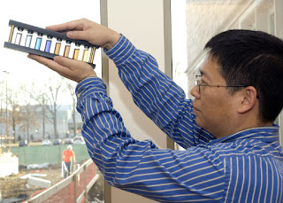
The new mechanical design strategy is based on semiconductor nanomaterials that can offer high stretchability (e.g., 140%) and large twistability such as corkscrew twists with tight pitch (e.g., 90o in 1cm). Potential uses for the new design include electronic devices for eye cameras, smart surgical gloves, body parts, airplane wings, back planes for liquid crystal displays and biomedical devises.

Stretchable Array

Caption: This picture shows an optical image of a freely deformed stretchable array of complementary metal-oxide semiconductors inverters.

Credit: Professor John A. Rogers and University of Illinois at Urbana-Champaign. Usage Restrictions: None.
"Our design is of great interest because the requirements for complex shapes that can function during stretching, compression, bending, twisting and other types of extreme mechanical deformation are impossible to satisfy with conventional technology," said Song.

The secret of the design is in the silicon (Si) islands on which the active devices or circuits are fabricated. The islands form a chemically bonded, pre-strained elastomeric substrate.
Releasing the pre-strain causes the metal interconnects of the circuits to buckle and form arc-shaped structures, which accommodate the deformation and make the semiconductor materials much more stretchable, without inducing significant changes in their electrical properties. The design is called noncoplanar mesh design.

The study is featured in the cover of the December issue of the Proceedings of the National Academy of Sciences (PNAS) and was selected for the special section of the journal called "In this issue." The work is titled "Materials and Noncoplanar Mesh Designs for Integrated Circuits with Linear Elastic Responses to Extreme Mechanical Deformations". The study describes a design system that can be stretched or compressed to high levels of strain, in any direction or combination of directions, with electronic properties that are independent of such strain, even in extreme arrangements. These types of systems might enable new applications not possible with current methods. ###

The University of Miami's mission is to educate and nurture students, to create knowledge, and to provide service to our community and beyond. Committed to excellence and proud of the diversity of our University family, we strive to develop future leaders of our nation and the world. www.miami.edu

Contact: Marie Guma-Diaz m.gumadiaz@umiami.edu 305-284-1601 University of Miami

Wednesday, February 25, 2009

Light-speed nanotech: Controlling the nature of graphene

Researchers 'tune' graphene's properties by growing it on different surfaces.

Troy, N.Y. – Researchers at Rensselaer Polytechnic Institute have discovered a new method for controlling the nature of graphene, bringing academia and industry potentially one step closer to realizing the mass production of graphene-based nanoelectronics.

Graphene, a one-atom-thick sheet of carbon, was discovered in 2004 and is considered a potential heir to copper and silicon as the fundamental building blocks of nanoelectronics.

With help from an underlying substrate, researchers for the first time have demonstrated the ability to control the nature of graphene.

two sheets of graphene

Caption: Researchers at Rensselaer have developed a new method for controlling the conductive nature of graphene. Pictured is a rendering of two sheets of graphene, each with the thickness of just a single carbon atom, resting on top of a silicon dioxide substrate.

Credit: Rensselaer/Shemella. Usage Restrictions: Include photo credit.
Saroj Nayak, an associate professor in Rensselaer's Department of Physics, Applied Physics, and Astronomy, along with Philip Shemella, a postdoctoral research associate in the same department, have determined that the chemistry of the surface on which graphene is deposited plays a key role in shaping the material's conductive properties. The results are based on large-scale quantum mechanical simulations.

Results show that when deposited on a surface treated with oxygen, graphene exhibits semiconductor properties. When deposited on a material treated with hydrogen, however, graphene exhibits metallic properties.
"Depending on the chemistry of the surface, we can control the nature of the graphene to be metallic or semiconductor," Nayak said. "Essentially, we are 'tuning' the electrical properties of material to suit our needs."

Conventionally, whenever a batch of graphene nanostructures is produced, some of the graphene is metallic, while the rest is semiconductor. It would be nearly impossible to separate the two on a large scale, Nayak said, yet realizing new graphene devices would require that they be comprised solely of metallic or semiconductor graphene. The new method for "tuning" the nature of graphene is a key step to making this possible, he said.

Graphene's excellent conductive properties make it attractive to researchers. Even at room temperature, electrons pass through the material effortlessly, near the speed of light and with little resistance. This means a graphene interconnect would likely stay much cooler than a copper interconnect of the same size. Cooler is better, as heat produced by interconnects can have negative effects on both a computer chip's speed and performance. ###

Results of the study were published this week in the paper "Electronic structure and band-gap modulation of graphene via substrate surface chemistry" in Applied Physics Letters, and are featured on the cover of the journal's January 19 issue.

Large-scale quantum simulations for the study were run on Rensselaer's supercomputing system, the Computational Center for Nanotechnology Innovations (CCNI).

Researchers received funding for the project from the New York State Interconnect Focus Center at Rensselaer.

Contact: Michael Mullaney mullam@rpi.edu 518-276-6161 Rensselaer Polytechnic Institute

Tuesday, February 24, 2009

Semiconducting nanotubes produced in quantity at Duke

DURHAM, N.C. -- After announcing last April a method for growing exceptionally long, straight, numerous and well-aligned carbon cylinders only a few atoms thick, a Duke University-led team of chemists has now modified that process to create exclusively semiconducting versions of these single-walled carbon nanotubes.

The achievement paves the way for manufacturing reliable electronic nanocircuits at the ultra-small billionths of a meter scale, said Jie Liu, Duke's Jerry G. and Patricia Crawford Hubbard Professor of Chemistry, who headed the effort.

"I think it's the holy grail for the field," Liu said. "Every piece is now there, including the control of location, orientation and electronic properties all together. We are positioned to make large numbers of electronic devices such as high-current field-effect transistors and sensors."

Dr. Jie Liu

Dr. Jie Liu, Jerry G. and Patricia Crawford Hubbard Professor of Chemistry. Duke University. 3218 French Family Science Center. Durham, NC, 27708-0354. Tel: (919) 660-1549, Fax: (919)660-1605, Email: j.liu@duke.edu
A report on their achievement, co-authored by Liu and a team of collaborators from his Duke laboratory and Peking University in China, was published Jan 20, 2009 in the research journal Nano Letters. Their work was funded by the United States Naval Research Laboratory, the National Science Foundation of China, carbon nanotube manufacturer Unidym Inc., Duke University and the Ministry of Science and Technology of the People's Republic of China.
Liu has filed for a patent on the method. A post doctoral researcher in his laboratory, Lei Ding, was first author of the new report as well as the previous study http://news.duke.edu/2008/04/stnanotubes.html published April 16, 2008, in the Journal of the American Chemical Society (JACS).

That earlier JACS report described how the researchers coaxed forests of nanotubes to form in long, parallel paths that will not cross each other to impede potential electronic performance. Their method grows the nanotubes on a template made of a continuous and unbroken kind of single quartz crystal used in electronic applications. Copper is also used as a growth promoter.

Carbon nanotubes are sometimes called "buckytubes" because their ends, when closed, take the form of soccer ball-shaped carbon-60 molecules known as buckminsterfullerines, or "buckyballs." The late Richard Smalley, who headed the Rice University laboratory where Liu was based before coming to Duke, shared a Nobel Prize for synthesizing buckyballs.

In addition to being especially tiny, those nanotubes offer other advantages -- including reduced heat output and higher frequency operation -- over current materials used to make miniaturized electronic components such as transistors, said Liu. "Operating at higher frequencies means they would be much better devices for wireless communications," he added.

But the April 2008 JACS report left one unresolved issue blocking use of such numerous, straight and well-aligned nanotubes as electronic components. Only some of the resulting nanotubes acted electronically as semiconductors. Others were the electronic equivalent of metals. To work in transistors, the nanotubes must all be semiconducting, Liu said.

In their new Nano Letters report, the researchers announced success at achieving virtually all-semiconductor growth conditions by making one modification. In their earlier work they had used the alcohol ethanol in the feeder gas to provide carbon atoms as building blocks for the growing nanotubes. In the new work they tried various ratios of two alcohols -- ethanol and methanol -- combined with two other gases they also used previously -- argon and hydrogen.

"We found that by using the right combination of the two alcohols with the argon and hydrogen we could grow exclusively semiconducting nanotubes," Liu said. "It was like operating a tuning knob." Chemically inert argon gas was used to provide a steady feed of the ethanol and methanol, with hydrogen to keep the copper catalyst from oxidizing.

After making the nanotubes by the chemical vapor deposition method in a small furnace set to a temperature of 900 degrees Celsius, the researchers assembled some of them into field-effect transistors to test their electronic properties.

"We have estimated from these measurements that the samples consisted of 95 to 98 percent semiconducting nanotubes," the researchers reported.

As a double-check, the scientists also subjected some nanotubes to Raman spectroscopy, an analytical technique that can differentiate semiconducting and metallic properties by studying how materials interact with various types of lasers.

According to the new Nano Letters report, the introduction of methanol to complement ethanol also shrunk the diameters of the resulting nanotubes and improved their atomic alignments with the underlying quartz crystal.

The resulting nanotubes can only be seen with exceptionally high magnification devices like scanning electron and atomic force microscopes. Whether the hollow carbon cylinders are metallic or semiconducting is a matter of their three dimensional alignments in space -- a trait scientists call "chirality."

The group's next challenge will be to understand at an atomic level how "just so" tuning of growth gas mixtures resulted in the right chirality to produce exclusively semiconducting nanotubes. The researchers are also wondering whether another combination might produce all-metallic nanotubes.

"We want to be able to control that chirality," he said. ###

Other authors of the Nano Letters report include Alexander Tselev, Dongning Yuan and Thomas McNicholas at Duke, and Yan Li, Jinyong Wang and Haibin Chu at Peking University.

Contact: Monte Basgall monte.basgall@duke.edu 919-681-8057 Duke University

Sunday, February 22, 2009

Microbot motors fit to swim human arteries

A range of complex surgical operations necessary to treat stroke victims, confront hardened arteries or address blockages in the bloodstream are about to be made safer as researchers from the Micro/Nanophysics Research Laboratory at Australia's Monash University put the final touches to the design of micro-motors small enough to be injected into the human bloodstream.

A research paper, published today, Tuesday, 20 January, in IOP Publishing's Journal of Micromechanics and Microengineering details how researchers are harnessing piezoelectricity, the energy force most commonly used to trigger-start a gas stove, to produce microbot motors just 250 micrometres, a quarter of a millimetre, wide.

MicrobotMethods of minimally invasive surgery, such as keyhole surgery and a range of operations that utilise catheters, tubes inserted into body cavities to allow surgical manoeuvrability, are preferred by surgeons and patients because of the damage avoided when contrasted against cut and sew operations.
Serious damage during minimally invasive surgery is however not always avoidable and surgeons are often limited by, for example, the width of a catheter tube which, in serious cases, can fatally puncture narrow arteries.

Remote controlled miniature robots small enough to swim up arteries could save lives by reaching parts of the body, like a stroke-damaged cranial artery, that catheters have previously been unable to reach (because of the labyrinthine structure of the brain that catheters are too immobile to safely reach). With the right sensor equipment attached to the microbot motor, the surgeon's view of, for example, a patient's troubled artery can be enhanced and the ability to work remotely also increases the surgeon's dexterity.
As Professor James Friend, leader of the research team at Monash University, explained, motors have lagged behind in the age of technological miniaturisation and provide the key to making robots small enough for injection into the bloodstream. "If you pick up an electronics catalogue, you'll find all sorts of sensors, LEDs, memory chips, etc that represent the latest in technology and miniaturisation. Take a look however at the motors and there are few changes from the motors available in the 1950s."

Professor Friend and his team began their research over two years ago in the belief that piezoelectricity was the most suitable energy force for micro-motors because the engines can be scaled down while remaining forceful enough, even at the sizes necessary to enter the bloodstream, for motors to swim against the blood's current and reach spots difficult to operate upon.

Piezoelectricity is most commonly found in quartz watches and gas stoves. It is based on the ability of some materials to generate electric potential in response to mechanical stress. In the case of a gas stove, the ignition switch on a stove triggers a spring to release a ball that smashes against a piece of piezoelectric material, often kinds of crystal, which translates the force of the ball into more than 10,000 volts of electricity which then travels down wires, reaches the gas, and starts the stove fire.

As Professor Friend explains, "Opportunities for micro-motors abound in fields as diverse as biomedicine, electronics, aeronautics and the automotive industry. Responses to this need have been just as diverse, with designs developed using electromagnetic, electrostatic, thermal and osmotic driving forces. Piezoelectric designs however have favourable scaling characteristics and, in general, are simple designs, which have provided an excellent platform for the development of micro-motors."

The team has produced prototypes of the motors and is now working on ways to improve the assembly method and the mechanical device which moves and controls the micro-motors. ###

Contact: Joe Winters joseph.winters@iop.org 0044-020-747-04815 Institute of Physics

Friday, February 20, 2009

Molecular forklifts overcome obstacle to ‘smart dust’ VIDEO

GAINESVILLE, Fla. — Algae is a livid green giveaway of nutrient pollution in a lake. Scientists would love to reproduce that action in tiny particles that would turn different colors if exposed to biological weapons, food spoilage or signs of poor health in the blood.

Now, University of Florida engineering researchers have tapped the working parts of cells to clear a major hurdle to creating such “smart dust.”

The feat, which signifies a new approach to technology known as the “lab on a chip,” is to be reported Sunday in the journal Nature Nanotechnology.

New smart dust image
“Instead of just changing one part of an existing system, we have a new and different way of doing things,” said Henry Hess, a UF assistant professor of materials science and engineering and the senior author of the paper. “And we can do it this way because of building blocks from bionanotechnology, and that’s what makes it very exciting.”

Chip-based labs have been developed in recent years as portable tools to gauge the presence of bioweapons, pollution, or to conduct on-the-spot blood tests. They are essentially assays, or ways to test for different pathogens, chemicals or compounds.
Scientists have suggested that the ever-shrinking labs could be reduced to the size of tiny particles of “smart” dust. But although today’s versions may be small, they require equipment that is hand-held at its smallest, and often large enough to require a lab bench.
“It’s like a computer,” Hess said. “The central processing unit is the really interesting thing, but you need all this other stuff to make it work.”

The extra equipment is needed because the assay, which uses pairs of antibodies to latch onto target contaminants and the markers that give away their presence, requires repeated flushing with water. That requires pumps, which need power. To miniaturize the system, it’s necessary to build miniature pumps and batteries. But that’s a challenge, especially for miniaturization to the level required for individual pieces of smart dust, Hess said.

His research strips out all peripheral equipment by using an altogether unique and different approach: biologically powered molecular forklifts.

The forklifts are assembled from natural motor proteins that are active in cell division. Hess and his team’s main innovation is manipulating these tiny proteins to perform heavy lifting and transport tasks — tasks that lead to a successful assay.

For a system rooted in biology, the process is uncannily mechanical.

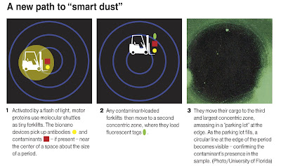
Using standard laboratory methods, the researchers squirt the forklifts into the central zone of three-zone circular surface no larger than the period at the end of this sentence. They then attach the same antibodies used in traditional chip-based labs.

When the surface is exposed to a contaminant, the antibodies latch onto it, just as happens with traditional assays. But then, activated by a flash of light, molecular shuttles start pushing the forklifts into a second zone, where they load aboard fluorescent particles, or tags. They move their cargo to the third zone, at the edge of the circle. There, over several hours, they crowd against each other, accumulating to the point where their combined loads form a line visible under magnification — and providing the telltale indicator of the contaminant.

The process requires no rinsing. And instead of electricity, the naturally derived forklifts are powered by adenosine triphosphate, or ATP, the molecule that carries energy for cells.

“You have replaced all this washing with this active transport by molecular shuttles, so you don’t need a pump or battery,” Hess said.

Michael Sailor, a professor of chemistry and biochemistry at the University of California San Diego and prominent smart-dust researcher, called the research “quite promising.”

“The key advance is that the authors incorporate a transport mechanism derived from a natural system into an artificial microsensor,” he wrote in an e-mail. “The authors show how adding the ability to move around in an autonomous fashion can dramatically improve the performance of the microsensor.”

Hess emphasized that the research results represent only the initial of many steps toward smart dust. Among other challenges, the molecular forklifts need to be sped up, producing results in seconds or minutes rather than hours. But, he said, the process suggests that there are promising, alternative to traditional lab-on-a-chip assays.

“Right now, this is light years away from competing with any assay,” he said. “But, it is a completely different way of doing it.”

The other authors of the paper are Thorsten Fischer, a former UF postdoctoral associate, and Ashutosh Agarwai, a doctoral student in Hess’ lab. The research was funded primarily by the Defense Advanced Research Projects Agency, with additional support from the Office of Naval Research and the UF Center for Sensor Materials and Technologies in the College of Engineering.

Credits: Writer Aaron Hoover, ahoover@ufl.edu, 352-392-0186. Source: Henry Hess, hhess@mse.ufl.edu, 352-846-3781; cell, 352-281-1661

Thursday, February 19, 2009

Spallation Neutron Source gets initial go-ahead on second target

OAK RIDGE, Tenn., Jan. 16, 2009 -- The U.S. Department of Energy has given its initial approval to begin plans for a second target station for the Spallation Neutron Source, expanding what is already the world's most powerful pulsed neutron scattering facility located at DOE's Oak Ridge National Laboratory.

The Critical Decision Zero (CD-0) status is the first step in an approximately $1 billion construction project. The Second Target Station (STS) will be optimized for nanoscale and biological sciences with an emphasis on novel materials for energy production, storage and use.

"The approval of CD-0 and the mission need statement for the STS reflects the Department's commitment to securing and expanding this Nation's leadership position in neutron science,"

Spallation Neutron Source

The Department of Energy has given initial approval to begin plans for the Second Target Station at SNS, depicted in the image here.
said Harriet Kung, DOE Associate Director of Science for Basic Energy Sciences.

With the addition of up to 24 instruments, the number of researchers that will have access to the SNS's unique neutron scattering capability will eventually double from 2,000 to 4,000 annually.
"CD-0 approval is great news for materials research. The second target station will expand the Spallation Neutron Source's capability for studying structure and dynamics on the nanoscale and provide for a growing community of users, maximizing the scientific investment in the SNS accelerator complex," said ORNL Director Thom Mason, who previously led the SNS project through most of its construction and startup phases.

The new target station-- the most intense source of its kind in the world--will generate long pulses of "cold" neutrons, which are cryogenically chilled to wavelengths that are more useful for molecular-scale analysis.

"The added suite of instruments will provide new research opportunities in technologically significant areas. With the SNS's new capabilities for studying materials and processes at the micro- and nanoscale, researchers will have the tools to develop new materials for a broad range of applications including advanced automotive battery technology, new steel alloys and pharmaceuticals," said Ian Anderson, ORNL Associate Laboratory Director for Neutron Sciences.

Research at the first target station at SNS, which has 10 instruments either operating or in commissioning, has already provided new insight into the behavior of materials used for the efficient transmission of electricity, and has facilitated the development of new methods of administering medicines.

As home of the SNS and the recently upgraded High Flux Isotope Reactor, ORNL is the world's leading center for neutron science. ###

CD-0 is the first of five "critical decisions" that govern construction of DOE facilities and projects, and is required before the development of a conceptual design study and submission of a budget request for the start of project engineering and design efforts. The project completion is estimated for 2020.

ORNL is managed by UT-Battelle for the Department of Energy. Funding for the STS is through the Department's Office of Science (Office of Basic Energy Sciences).

Contact: Bill Cabage cabagewh@ornl.gov 865-574-4399 DOE/Oak Ridge National Laboratory

Wednesday, February 18, 2009

A fantastic voyage brought to life

Ever since the 1966 Hollywood movie, doctors have imagined a real-life Fantastic Voyage –– a medical vehicle shrunk small enough to "submarine" in and fix faulty cells in the body. Thanks to new research by Tel Aviv University scientists, that reality may be only three years away.

The blueprints for the submarine and a map of its proposed maiden voyage were published earlier this year in Science by Dr. Dan Peer, who now leads the Tel Aviv University team at the Department of Cell Research and Immunology. The team will build and test-run the actual "machine" in human bodies. Dr. Peer originally developed the scenario at Harvard University.

Dr. Dan Peer

Caption: Dr. Dan Peer is a researcher with Tel Aviv University. Credit: AFTAU. Usage Restrictions: None.
Made from biological materials, the real-life medical submarine's Fantastic Voyage won't have enough room for Raquel Welch, but the nano-sized structure will be big enough to deliver the payload: effective drugs to kill cancer cells and eradicate faulty proteins.

A Nano-GPS System

"Our lab is creating biological nano-machines," says Dr. Peer. "These machines can target specific cells. In fact, we can target any protein that might be causing disease or disorder in the human body. This new invention treats the source, not the symptoms."
Dr. Peer's recent paper reported on the device's ability to target leukocytes (immune cells) in the guts of mice with ulcerative colitis. Calling his new invention a submarine, Dr. Peer has developed a nano-sized carrier which operates like a GPS system to locate and target cells. In the case of Crohn's disease, for example, it will target overactive immune system cells in the gut. In other diseases such as cancer, the submarine can aim for and deliver material to specific cancer cells, leaving the surrounding healthy cells intact.

While other researchers are working in the area of nano-medicine and drug delivery, Dr. Peer's submarines are among the first to combine a drug candidate with a drug delivery system. As the submarines float through the body, they latch onto the target cell and deliver their payload, a drug based on RNAi. This new kind of drug can affect faulty RNA machinery and reprogram cells to operate in normal ways. In essence, RNAi can essentially restore health to diseased cells or cause cells to die (like in the case of cancer cells).

Learning from the Body's Own System
Large pharmaceutical companies have already expressed interest in this research and in the area of RNAi in general. Currently, the Tel Aviv University lab is pairing its medical submarine with different RNAi compounds to target different pathologies, such as cancer, inflammation, and neurodegenerative diseases.nanoparticle decorated with targeting agents

Caption: A nanoparticle decorated with targeting agents that guide it to a specific cell type, leaving healthy cells untouched. Credit: AFTAU. Usage Restrictions: None.
"We have tapped into the same ancient system the human body uses to protect itself from viruses," says Dr. Peer, who is also investigating a number of topical applications for his medical subs. "And the beauty of it is the basic material of our nano-carriers is natural," he says.

The Tel Aviv University team plans to launch their medical submarines, following FDA regulations, within three to five years. Their immediate focus is on blood, pancreatic, breast and brain cancers. ###

The researchers are currently collaborating with a number of teams around the world. In the area of breast cancer, they are working with researchers from Harvard University and MIT. In blood cancers, collaboration with the Dana-Farber Cancer Institute at Harvard Medical School is already progressing towards clinical trials.

American Friends of Tel Aviv University (www.aftau.org) supports Israel's leading and most comprehensive center of higher learning. In independent rankings, TAU's innovations and discoveries are cited more often by the global scientific community than all but 20 other universities worldwide.

Internationally recognized for the scope and groundbreaking nature of its research programs, Tel Aviv University consistently produces work with profound implications for the future.

Contact: George Hunka ghunka@aftau.org 212-742-9070 American Friends of Tel Aviv University

Tuesday, February 17, 2009

Easy assembly of electronic biological chips

A handheld, ultra-portable device that can recognize and immediately report on a wide variety of environmental or medical compounds may eventually be possible, using a method that incorporates a mixture of biologically tagged nanowires onto integrated circuit chips, according to Penn State researchers.

"Probably one of the most important things for connecting to the circuit is to place the wires accurately," says Theresa S. Mayer, professor of electrical engineering and director of Penn State's Nanofabrication Laboratory. "We need to control spatial placement on the chip with less than a micron of accuracy."

Using standard chip manufacturing, each type of nanowire would be placed on the board in a separate operation.

Assembled Nanowires

Caption: These nanowires, tagged with DNA are assembled, and have been exposed to complementary DNA that is tagged with fluorescent dyes. The complementary DNA attached to the nanowires showing that the wires assembled in the proper locations.

Credit: Penn State. Usage Restrictions: Non-advertising use only

Nanowire Pile

Caption: This is a pile of nanowires before assembly. Credit: Penn State, Usage Restrictions: Non-advertising use only.
Using the researchers' bottom-up method, they can place three different types of DNA-coated wires where they wanted them, with an error rate of less than 1 percent.

"This approach can be used to simultaneously detect different pathogens or diseases based on their nucleic acid signatures," says Christine D. Keating, associate professor of chemistry.

"Device components such as nanowires can be synthesized from many different materials and even coated with biological molecules prior to assembling them onto a chip," the researchers note in today's (Jan. 16) issue of Science. They add that positioning the nanowires accurately is still difficult using conventional methods.

Using their assembly method, the researchers can place specific nanowires in assigned areas. They begin with a chip with tiny rectangular depressions in the places they wish to place the nanowires. They then apply an electrical field between electrodes that define the area where they want the nanowires to assemble. The Penn State researchers inject a mixture of the tagged nanowires and a liquid over the top of the chip. The nanowires are attracted to the area with an electric field and they fall into the proper tiny wells.
"We do not need microfluidic channels to control where each nanowire type goes," says Mayer. "We can run the solution over the whole chip and its wires will only attach where they are supposed to attach. This is important for scale-up."

The researchers then move the electric field and position the next tagged nanowires. In this proof-of-concept experiment, the different tagged wires were placed in rows, but the researchers say that they could be placed in a variety of configurations.

After all the wires are in place, they can be made into a variety of devices including resonators or field effect transistors that can be used to detect nucleic acid targets.

While the researchers have not yet connected each individual device to the underlying circuitry, they did test their chip to ensure that the wires assembled in the proper locations. They immersed the chip in a solution containing DNA sequences complementary to the three virus-specific sequences on the nanowires. Because they tagged the complimentary DNA with three differently colored fluorescent dyes, the attached DNA showed that the wires were in the proper places.

The researchers believe that their assembly method is extremely flexible, capable of placing a variety of conducting and non-conducting wires with a wide array of coatings.

"The eventual idea would be to extend the method to more nanowire types, such as different DNA sequences or even proteins, and move from fluorescence to real-time electrical detection on the chip," says Keating. ###

Researchers working on this project include Mayer; Keating; Thomas J. Morrow, graduate student in chemistry; Jaekyun Kim, graduate student in electrical engineering; and Mingwei Li, recent graduate student in electrical engineering. The National Science Foundation and the National Institutes of Health supported this work.

Contact: A'ndrea Elyse Messer aem1@psu.edu 814-865-9481 Penn State

Monday, February 16, 2009

U of T chemistry discovery brings organic solar cells a step closer

Inexpensive solar cells, vastly improved medical imaging techniques and lighter and more flexible television screens are among the potential applications envisioned for organic electronics.

Recent experiments conducted by Greg Scholes and Elisabetta Collini of University of Toronto's Department of Chemistry may bring these within closer reach thanks to new insights into the way molecules absorb and move energy. Their findings will be published in the prestigious international journal Science on January 16.

The U of T team -- whose work is devoted to investigating how light initiates physical processes at the molecular level and how humans might take better advantage of that fact -- looked specifically at conjugated polymers which are believed to be one of the most promising candidates for building efficient organic solar cells.

Conjugated polymers are very long organic molecules that possess properties like those of semiconductors and so can be used to make transistors and LEDs. When these conductive polymers absorb light, the energy moves along and among the polymer chains before it is converted to electrical charges.

Gregory Scholes Associate Professor

Gregory Scholes Associate Professor
"One of the biggest obstacles to organic solar cells is that it is difficult to control what happens after light is absorbed: whether the desired property is transmitting energy, storing information or emitting light," explains Collini. "Our experiment suggests it is possible to achieve control using quantum effects, even under relatively normal conditions."

"We found that the ultrafast movement of energy through and between molecules happens by a quantum-mechanical mechanism rather than through random hopping, even at room temperature," explains Scholes.
"This is extraordinary and will greatly influence future work in the field because everyone thought that these kinds of quantum effects could only operate in complex systems at very low temperatures," he says.

Scholes and Collini's discovery opens the way to designing organic solar cells or sensors that capture light and transfer its energy much more effectively. It also has significant implications for quantum computing because it suggests that quantum information may survive significantly longer than previously believed.

In their experiment, the scientists used ultrashort laser pulses to put the conjugated polymer into a quantum-mechanical state, whereby it is simultaneously in the ground (normal) state and a state where light has been absorbed. This is called a superposition state or quantum coherence. Then they used a sophisticated method involving more ultrashort laser pulses to observe whether this quantum state can migrate along or between polymer chains. "It turns out that it only moves along polymer chains," says Scholes. "The chemical framework that makes up the chain is a crucial ingredient for enabling quantum coherent energy transfer. In the absence of the chemical framework, energy is funneled by chance, rather than design."

This means that a chemical property – structure -- can be used to steer the ultrafast migration of energy using quantum coherence. The unique properties of conjugated polymers continue to surprise us," he says. ###

Greg Scholes and Elisabetta Collini are with the Department of Chemistry, the Institute for Optical Sciences and the Centre for Quantum Information and Quantum Control at the University of Toronto. The research was funded by the Natural Sciences and Engineering Research Council of Canada.

CONTACT:
  • Greg Scholes, Department of Chemistry, University of Toronto. 416-946-7532 (office) 416-333-0044 (cell) gscholes@chem.utoronto.ca Note: Between January 12 – 16, Prof. Scholes is best reached on email.
  • Elisabetta Collini, Department of Chemistry, University of Toronto, 416- 946-7633 ecollini@chem.utoronto.ca
  • Kim Luke, Communications, Faculty of Arts & Science, University of Toronto, 416-978-4352. kim.luke@utoronto.ca
Contact: kim.luke@utoronto.ca kim.luke@utoronto.ca 416-978-4352 University of Toronto

Sunday, February 15, 2009

Super-sensitive gas detector goes down the nanotubes

When cells are under stress, they blow off steam by releasing minute amounts of nitrogen oxides and other toxic gases. In a recent paper,* researchers at the National Institute of Standards and Technology (NIST) described a new method for creating gas detectors so sensitive that some day they may be able to register these tiny emissions from a single cell, providing a new way to determine if drugs or nanoparticles harm cells or to study how cells communicate with one another. Based on metal oxide nanotubes, the new sensors are a hundred to 1,000 times more sensitive than current devices based on thin films and are able to act as multiple sensors simultaneously.

Gas sensors often operate by detecting the subtle changes that deposited gas molecules make in the way electricity moves through a surface layer.

Super-Sensitive Gas Detector

Caption: NIST researchers have developed a new technique to form nanotubes for use in gas sensing applications. One hundred to 1,000 times more sensitive than comparable sensors, their device could be used to study biological cell stress and cell communication.

Credit: NIST. Usage Restrictions: None.
Thus, the more surface available, the more sensitive the sensor will be. Scientists are interested in developing gas sensors based on nanotubes because, having walls that are only a few nanometers thick, they are almost all surface.

Although nanotubes have proven to be well suited for gas sensing applications, fabricating the devices themselves is a difficult, imprecise and time-consuming process, according to Kurt Benkstein, an author of the paper.
Older methods include randomly scattering free nanotubes on a surface with preformed electrical contacts (the hope being that a least a few of the nanotubes would tumble into place) or laying contacts over the top of the nanotubes after they had been dispersed, among others. These methods, though they can result in functional devices, preclude researchers from knowing where exactly the reactions are happening on the substrate. This makes it impossible to do multiple simultaneous tests. Also, these sensors are not as sensitive as they could be because there is no way to ensure that the gas is reacting with the interior of the tube.

To address these problems, the NIST group built upon another design using a sheet of aluminum oxide about the thickness of a human hair and perforated with millions of holes about 200 nanometers wide. With the nanosized pores serving as a mold, the researchers dipped the aluminum oxide sheet in a solution of tungsten ions, coating the interior of the pores and casting the nanotubes in place. After the nanotubes were formed, the team deposited thin layers of gold on the top and bottom of the aluminum oxide membrane to act as electrical contacts. View schematic of the nanotube sensor at http://patapsco.nist.gov/ImageGallery/details.cfm?imageid=620.

The sensor’s high sensitivity derives from its design, which ensures that any sensor response is the result of the gas interacting with the interior of the nanotube. The researchers also note that this same technique can easily be adapted to form nanotubes of other semiconductors and metal oxides so long as the ends of the nanotubes remain open. ###

* R. Artzi-Gerlitz, K. Benkstein, D. Lahr, J. Hertz, C. Montgomery, J. Bonevich, S. Semancik, M. Tarlov. Fabrication and gas sensing performance of parallel assemblies of metal oxide nanotubes supported by porous aluminum oxide membranes. Sensors and Actuators B: Chemical. Available online Nov. 11, 2008.

Contact: Mark Esser mark.esser@nist.gov 301-975-8735 National Institute of Standards and Technology (NIST)

Saturday, February 14, 2009

'2-faced' bioacids put a new face on carbon nanotube self-assembly

Nanotubes, the tiny honeycomb cylinders of carbon atoms only a few nanometers wide, are perhaps the signature material of modern engineering research, but actually trying to organize the atomic scale rods is notoriously like herding cats. A new study* from the National Institute of Standards and Technology (NIST) and Rice University, however, offers an inexpensive process that gets nanotubes to obediently line themselves up—that is, self-assemble—in neat rows, more like ducks.

A broad range of emerging electronic and materials technologies take advantage of the unique physical, optical and electrical properties of carbon nanotubes, but most of them—nanoscale conductors or “nanowires,” for instance—are predicated on the ability to efficiently line the nanotubes up in some organized arrangement.

Carbon Nanotube Self-Assembly

Caption: Single wall carbon nanotubes enclosed in bile acid shells self assembled into a sheaf of long ordered fibrils each composed of several nanotube rods. Treating the microscope slide with a hydrophobic compound causes the fibrils to cluster like this at specific sites, probably at defects in the hydrophobic surface. Image, 70 micrometers wide, was taken using near-infrared fluorescent microscopy. (Color added for clarity.)

Credit: NIST. Usage Restrictions: None.
Unfortunately, just mixed in a solvent, the nanotubes will clump together in a black goo. They can be coated with another molecule to prevent clumping—DNA is sometimes used—but spread the mixture out and dry it and you get a random, tangled mat of nanotubes. There have been a variety of mechanical approaches to orienting carbon nanotubes on a surface (see, for example, “NIST’s Stretching Exercises Shed New Light on Nanotubes,” Tech Beat, Apr. 12, 2007: http://www.nist.gov/public_affairs/techbeat/tb2007_0412.htm#nanotubes ), but a more elegant and attractive solution would be to get them to do it themselves—self assembly.
NIST researchers studying better ways to sort and purify carbon nanotubes to prepare standard samples of the material were using a bile acid** to coat the nanotubes to prevent clumping. “Bile acids,” says NIST research chemist Erik Hobbie, “are biological surfactants, and like most surfactants they have a part that likes water and a part that doesn’t. This is a slightly complex surfactant because instead of having a head and a tail, the usual geometry, it has two faces, one that likes water and one that doesn’t.” Mixed in water, such hydrophobic/hydrophilic molecules normally want to group together in hollow spheres with their hydrophobic “tails” sheltered on the inside, Hobbie explains, but the two-faced geometry of this bile acid makes it form hollow rod shapes instead. Conveniently, the hollow rods can house the rod-shaped nanotubes.

As it turns out, there’s a bonus. Over the course of about a day, the bile acid shells cause the nanotubes to begin lining up, end to end, in long strands, and then the strands begin to join together in twisted filaments, like a length of twisted copper wire. The discovery is a long way from a perfect solution for ordering nanotubes, Hobbie cautions, and a lot of development remains to be done. For one thing, ideally, the bile acid shells would be removed after the nanotubes are in their ordered positions, but this has proven difficult. And the surfactant is toxic to living cells, which precludes most biomedical applications unless it is removed. On the other hand, he says, it already is an easy and extremely inexpensive technique for researchers interested in studying, for example, optical properties of carbon nanotubes. “It gives a recipe for how to create ordered, aligned arrangements of individual carbon nanotubes. You don’t need to use any external magnetic or electrical fields, and you don’t need to dry the tubes out in a polymer and heat it up and stretch it. You can get fairly significant regions of very nice alignment just spontaneously through this self assembly.” ###

(For more on the purifying of carbon nanotubes, see “Spin Control: New Technique Sorts Nanotubes by Length,” Tech Beat, May 13,2008: nist.gov/public_affairs/techbeat/nanotubes )

* E.K. Hobbie, J.A. Fagan, M.L. Becker, S.D. Hudson, N. Fakhri and M. Pasquali. Self-assembly of ordered nanowires in biological suspensions of single-wall carbon nanotubes. ACS Nano, published online Dec. 16, 2008.

** Sodium deoxycholate.

Contact: Michael Baum michael.baum@nist.gov 301-975-2763 National Institute of Standards and Technology (NIST)

Friday, February 13, 2009

Can you see me now? Flexible photodetectors could help sharpen photos

Distorted cell-phone photos and big, clunky telephoto lenses could be things of the past.

UW-Madison Electrical and Computer Engineering Associate Professor Zhenqiang (Jack) Ma and colleagues have developed a flexible light-sensitive material that could revolutionize photography and other imaging technologies.

Their technology is featured on the cover of the January issue of Applied Physics Letters.

When a device records an image, light passes through a lens and lands on a photodetector -- a light-sensitive material like the sensor in a digital camera.

curved photodetector array

This example of a curved photodetector array was developed by University of Wisconsin-Madison Electrical and Computer Engineering Associate Professor Zhenqiang (Jack) Ma and colleagues. Inspired by the human eye, Ma’s curved photodetector made of flexible germanium could eliminate the photo distortion that occurs in conventional photo lenses.

Photo: courtesy Zhenqiang Ma.
However, a lens bends the light and curves the focusing plane. In a digital camera, the point where the focusing plane meets the flat sensor will be in focus, but the image becomes more distorted the farther it is from that focus point.

"If I take a picture with a cell phone camera, for example, there is distortion," says Ma. "The closer the subject is to the lens, the more distortion there is."

That's why some photos can turn out looking like images in a funhouse mirror, with an enlarged nose or a hand as big as a head.

High-end digital cameras correct this problem by incorporating multiple panes of glass to refract light and flatten the focusing plane.
However, such lens systems -- like the mammoth telephoto lenses sports photographers use -- are large, bulky and expensive. Even high-quality lenses stretch the edges of an image somewhat.

Inspired by the human eye, Ma's curved photodetector could eliminate that distortion. In the eye, light enters though a single lens, but at the back of the eye, the image falls upon the curved retina, eliminating distortion. "If you can make a curved imaging plane, you just need one lens," says Ma. "That's why this development is extremely important."

Ma and his group can create curved photodetectors with specially fabricated nanomembranes -- extremely thin, flexible sheets of germanium, a very light-sensitive material often used in high-end imaging sensors. Researchers then can apply the nanomembranes to any polymer substrate, such as a thin, flexible piece of plastic. Currently, the group has demonstrated photodetectors curved in one direction, but Ma hopes next to develop hemispherical sensors.

"We can easily realize very high-density flexible and sensitive imaging arrays, because the photodetector material germanium itself is extremely bendable and extremely efficient in absorbing light," Ma adds.

Ma's co-authors include UW-Madison Materials Science and Engineering Professor Max Lagally and University of Michigan Professor Pallab Bhattacharya.

Contact: Zhenqiang (Jack) Ma mazq@engr.wisc.edu 608-261-1095 University of Wisconsin-Madison

Thursday, February 12, 2009

Novel technique changes lymph node biopsy, reduces radiation exposure

'Good as gold': Information obtained from a new application of photoacoustic tomography (PAT) is worth its weight in gold to breast cancer patients.

For the first time, Lihong Wang, Ph.D., Gene K. Beare Distinguished Professor in the Department of Biomedical Engineering, with a joint appointment in Radiology, and Younan Xia, Ph.D., James M. McKelvey Professor in Biomedical Engineering, with a joint appointment in chemistry in Arts & Sciences, both at Washington University in St. Louis, have used gold nanocages to map sentinel lymph nodes (SLN) in a rat noninvasively using PAT. Wang's lab is the largest PAT lab in the world credited with the invention of super-depth photoacoustic microscopy, and Xia's lab invented the gold nanocages.

biomedical engineers Younan Xia (left) and Lihong Wang

WUSTL biomedical engineers Younan Xia (left) and Lihong Wang examine the photoacoustic tomography machine (PAT) in Wang's Whitaker Building laboratory. Wang's lab is the largest PAT lab in the world, credited with the invention of super-depth photoacoustic microscopy. Xia's laboratory invented the gold nanocages. Wang and Xia have teamed together to apply gold nanocages and PAT to minimize invasive surgical lymph node biopsy procedures and reduce a patient's exposure to radioactivity.
Their work can minimize invasive surgical lymph node biopsy procedures to determine if breast cancer has metastasized and reduce the patient's exposure to radioactivity. The nanocages also have the potential to serve as an alternative to chemotherapy to kill targeted cancers by heating them up.

From heat, to expansion, to sound and an image

PAT blends optical and ultrasonic imaging to give high-resolution images of the body that contain information about physiology or tissue function.
Molecules already present in the body (endogenous molecules, as opposed to exogenous ones that are from outside the body), such as melanin, hemoglobin, or lipids, can be used as endogenous contrast agents for imaging. When light is shone on the tissue, the contrast agent absorbs the light, converts it to heat, and expands. This expansion is detected as sound and decoded into an image.

"Using pure optical imaging, it is hard to look deep into tissues at high resolution because light scatters. The useful photons run out of juice within 1mm," Wang explained. "PAT improves tissue transparency by 2-3 orders of magnitude because sound scatters less than light. This allows us to see through the tissue by listening to the sound."
Exogenous contrast agents, like the gold nanocages developed by Xia's group, can be used to image parts of the body that even contain endogenous contrast agents. These nanocages are especially attractive because their properties can be tuned to give optimal contrast and gold is non-toxic.

"By controlling the synthesis, we can move the absorption peak for the nanocages to a region that allows them to be imaged deep in tissue. We can also attach biomolecules to the surface of the nanocages so they are targeted to cancer cells," Xia said.
Younan Xia holds an array of glass vials

Younan Xia holds an array of glass vials containing many millions of gold nanocages in a Whitaker Building hallway. Xia's gold nanocages are making possible ways to image cancer cells in lymph tissue and some day could be used to carry biomolecules as attachments that could target cancer cells.
Safe imaging, no radioactivity or surgery

The SLN, the first draining node, is often biopsied in breast cancer patients to determine if the cancer has metastasized. "To find the SLN, doctors inject radioactive particles and a blue dye into the breast. The lymphatic system gobbles up the injected material, treating it as foreign matter and accumulating it in the SLN. The radioactive particles can be detected using a Geiger counter held to the breast to locate the lymph nodes. Then, the doctors surgically open the breast, follow the blue dye, and dissect the SLN," Wang said.

Wang and Xia's technique allows the SLN to be imaged safely without radioactivity or surgery. A piece of tissue can then be removed using a minimally invasive needle biopsy and tested for cancer. "We will convert an invasive surgical procedure into a minimally invasive needle biopsy," Wang said. ###

The work was supported by the National Institutes of Health.

In the future, they hope to attach molecules to the surface of the gold nanocages that will selectively bind to cancer cells, making a "smart contrast agent." Then, the nanocages will only be detected where cancer is present, eliminating the need for a needle biopsy.

Written by: Melissae Stuart

Contact: Lihong Wang lhwang@wustl.edu 31-493-593-56152 Washington University in St. Louis

Tuesday, February 10, 2009

Synthetic HDL: A new weapon to fight cholesterol problems

EVANSTON, Ill. --- Buttery Christmas cookies, eggnog, juicy beef roast, rich gravy and creamy New York-style cheesecake. Happy holiday food unfortunately can send blood cholesterol levels sky high.

Northwestern University scientists now offer a promising new weapon -- synthetic high-density lipoprotein (HDL), the "good" cholesterol -- that could help fight chronically high cholesterol levels and the deadly heart disease that often results.

The researchers successfully designed synthetic HDL and show that their nanoparticle version is capable of irreversibly binding cholesterol. The synthetic HDL, based on gold nanoparticles, is similar in size to HDL and mimics HDL's general surface composition.

synthetic HDL, based upon gold nanoparticle scaffolds

The synthetic HDL, based upon gold nanoparticle scaffolds, binds cholesterol and can potentially eat away at cholesterol-containing plaques. (Credit: Weston Daniel, David Giljohann and Michael Wiester, Mirkin Research Group)
The study is published online by the Journal of the American Chemical Society (JACS).

“We have designed and built a cholesterol sponge. The synthetic HDL features the basics of what a great cholesterol drug should be,” said Chad A. Mirkin, George B. Rathmann Professor of Chemistry in the Weinberg College of Arts and Sciences, professor of medicine and professor of materials science and engineering. Mirkin and Shad Thaxton, M.D., assistant professor of urology in Northwestern’s Feinberg School of Medicine, led the study.
"Drugs that lower the bad cholesterol, LDL, are available, and you can lower LDL through your diet, but it is difficult to raise the good cholesterol, HDL," said Mirkin. "I've taken niacin to try and raise my HDL, but the side effects are bad so I stopped. We are hopeful that our synthetic HDL will one day help fill this gap in useful therapeutics."

In creating synthetic HDL the researchers started with a gold nanoparticle as the core. They then layered on a lipid that attaches to the gold surface, then another lipid and last a protein, called APOA1, the main protein component of naturally occurring HDL. The final high-density lipoprotein nanoparticles are each about 18 nanometers in diameter, a size similar to natural HDL.

"Cholesterol is essential to our cells, but chronic excess can lead to dangerous plaque formation in our arteries," said Thaxton. "HDL transports cholesterol to the liver, which protects against atherosclerosis. Our hope is that, with further development, our synthetic form of HDL could be used to increase HDL levels and promote better health."

“HDL is a natural nanoparticle, and we’ve successfully mimicked it,” said Mirkin, director of Northwestern’s International Institute for Nanotechnology. “Gold is an ideal scaffolding material -- it’s size and shape can be tailored, and it can be easily functionalized. Using gold nanoparticles, which are non-toxic, for synthetic HDL bodes well for the development of a new therapeutic.”

The development of synthetic HDL is a result of a successful collaboration between scientists in Northwestern's department of chemistry and the Feinberg School. Bringing these two groups together, says Mirkin, should lead to major advances in translational research. Their next step is to further study the synthetic HDL in biologically relevant conditions and measure and evaluate the cholesterol-binding properties. ###

The work was supported by the NIH Director’s Pioneer Award (National Institutes of Health).

In addition to Mirkin and Thaxton, other authors of the JACS paper, titled “Templated Spherical High Density Lipoprotein Nanoparticles,” are Weston L. Daniel, David A. Giljohann and Audrey D. Thomas, all from Northwestern.

Contact: Megan Fellman fellman@northwestern.edu 847-491-3115 Northwestern University

Monday, February 09, 2009

URMC, Lighthouse Biosciences Awarded U.S. Patent for Diagnostic Technology

Lighthouse Biosciences' technology platform is focused on the field of hospital acquired infections.The University of Rochester Medical Center (URMC) has received a U.S. patent for a diagnostic technology that can rapidly and accurately screen for organisms such as bacteria and other infectious agents.Lighthouse Biosciences, Inc., a Rochester-based life sciences company, is the exclusive worldwide license holder of the technology.

The company’s technology platform – called NanoLantern – is a novel method of identifying genetic sequences from biological samples, a process that can be used to detect any organism or genetic feature by identifying its unique DNA fingerprint.

hospital acquired infections

Lighthouse Biosciences' technology platform is focused on the field of hospital acquired infections.
The NanoLantern consists of an array of DNA probes that can be programmed from a database of known genetic signatures to simultaneously screen for multiple individual targets using a single sample of blood, urine, cells, or other substance with organic content.The U.S. patent is being awarded for the process the technology uses to identify DNA sequences. The method, first developed by University of Rochester scientists in 2003, promises to be faster and more precise than other existing models.
“This patent represents an important milestone in developing the company’s intellectual property portfolio,” said Rand Henke, CEO of Lighthouse Bioscience.“It addresses a breakthrough method that will allow the company to design and make at a low cost a very wide range of probes for the detection of most pathogens.”

The company is in the process of developing a prototype that consists of a series of disposable biosensor cartridges – or labs on a chip – that will be housed in a workstation that can be deployed in hospitals, doctor’s offices, nursing homes, or any other health care setting.

While the technology has a wide array of potential applications in healthcare, agriculture, food safety, water quality, and national security, Lighthouse Biosciences is initially focused on the field of hospital-acquired infections (HAI).HAI are infections that patients receive during their care – in a hospital or other health care facility such as a nursing home – that are not related to any preexisting medical condition.Despite extensive efforts in recent years to address the causes, HAI remain a massive burden on the U.S. health care system with more than 1 million annual cases and 90,000 associated deaths, at a cost to health care of $5.7 billon per year and approximately $30 billion per year in the U.S. in social costs.

One of the key challenges in combating HAI is the need to develop a system of surveillance that can identify these infections as early as possible.The current standard is to send potentially infectious samples out to a clinical laboratory for analysis and wait for the results. This process typically takes up 2 to 3 days depending upon the proximity of the lab to the health care facility and the speed at which the lab can process the samples, a delay that can be an impediment to successful treatment. The NanoLantern technology has demonstrated the ability to provide results rapidly – within 15 minutes – and do so at the point of care.

The largest category of HAIs is urinary tract infections, which account for 40% of all infections. Lighthouse Biosciences, in cooperation with the URMC Departments of Urology and Microbiology and Immunology is currently conducting clinical studies to test the screening system at URMC’s Strong Memorial Hospital.

The underlying technology for the company’s NanoLantern platform was first developed by University of Rochester scientists Benjamin Miller, Ph.D., Todd Krauss, Ph.D. and Christopher Strohsahl, Ph.D.In addition to faculty appointments at the University, all three also hold corporate positions and/or equity positions in the company.Lighthouse Biosciences L.L.C., which was founded by the scientists in 2005, is based in the Lennox Tech Enterprise Center in Henrietta.

Contact: Mark Michaud mark_michaud@urmc.rochester.edu 585-273-4790 University of Rochester Medical Center

Sunday, February 08, 2009

Researchers control the assembly of nanobristles into helical clusters

Finding has potential use in energy and information storage, photonics, adhesion, capture and release systems, and chemical mixing.

CAMBRIDGE, Mass. – From the structure of DNA to nautical rope to distant spiral galaxies, helical forms are as abundant as they are useful in nature and manufacturing alike. Researchers at the Harvard School of Engineering and Applied Sciences (SEAS) have discovered a way to synthesize and control the formation of nanobristles, akin to tiny hairs, into helical clusters and have further demonstrated the fabrication of such highly ordered clusters, built from similar coiled building blocks, over multiple scales and areas.

unclustered nanobristle

Caption: Scanning electron microscopy images showing the morphogenesis of helical patterns, from the first-order unclustered nanobristle to the fourth-order coiled bundle. Scale bars, 4 mm. Note the hierarchical nature of the assembly reflected in the presence of the lower-order braids in the large clusters braided in a unique structure reminiscent of modern dreadlocks or mythical Medusa.

Credit: Courtesy of the Aizenberg lab at the Harvard School of Engineering and Applied Sciences. Usage Restrictions: None.
The finding has potential use in energy and information storage, photonics, adhesion, capture and release systems, and as an enhancement for the mixing and transport of particles. Lead authors Joanna Aizenberg, Gordon McKay Professor of Materials Science at SEAS and the Susan S. and Kenneth L. Wallach Professor at the Radcliffe Institute for Advanced Study, and L Mahadevan, Lola England de Valpine Professor of Applied Mathematics at SEAS, reported the research in the January issue of Science.

"We demonstrated a fascinating phenomenon: How a nanobristle immersed in an evaporating liquid self-assembles into an ordered array of helical bundles.
This is akin to the way wet, curly hair clumps together and coils to form dreadlocks—but on a scale 1000 times smaller," said Aizenberg.

To achieve the "clumping" effect, the scientists used an evaporating liquid on a series of upright individual pillars arrayed like stiff threads on a needlepoint canvas. The resulting capillary forces—the wicking action or the ability of one substance to draw another substance into it—caused the individual strands to deform and to adhere to one another like braided hair, forming nanobristles.

"Our development of a simple theory allowed us to further characterize the combination of geometry and material properties that favor the adhesive, coiled self-organization of bundles and enabled us to quantify the conditions for self-assembly into structures with uniform, periodic patterns," said Mahadevan.
By carefully designing the specific geometry of the bristle, the researchers were able to control the twist direction (or handedness) of the wrapping of two or more strands. More broadly, Aizenberg and Mahadevan, who are both core members of the recently established Wyss Institute for Biologically Inspired Engineering at Harvard, expect such work will help further define the emerging science and engineering of functional self-assembly and pattern formation over large spatial scales.

Potential applications of the technique include the ability to store elastic energy and information embodied in adhesive patterns that can be created at will. This has implications for photonics in a similar way to how the chirally-ordered and circularly-polarizing elytral filaments in a beetle define its unique optical properties.
Bristles hugging a polystyrene sphere

Caption: Bristles hugging a polystyrene sphere.

Credit: Courtesy of Aizenberg lab at the Harvard School of Engineering and Applied Sciences. Usage Restrictions: None.
The finding also represents a critical step towards the development of an efficient adhesive or capture and release system for drug delivery and may be used to induce chiral flow patterns to enhance the mixing and transport of various particles at the micron- and submicron sale.

"We have teased apart and replicated a ubiquitous form in nature by introducing greater control over a technique increasingly used in manufacturing while also creating a micro-physical manifestation of the terrifying braids of the mythical Medusa," said Mahadevan.

"Indeed, our helical patterns are so amazingly aesthetic that often we would stop the scientific discussion and argue about mythology, modern dreadlocks, alien creatures, or sculptures," added Aizenberg. ###

Aizenberg and Mahadevan's co-authors included Boaz Pokroy and Sung H. Kang, both in the Aizenberg Biomimetics Lab at SEAS. The research was supported by the Wyss Institute for Biologically Inspired Engineering at Harvard; the Harvard Materials Research Science and Engineering Center; and the Center for Nanoscale Systems, a member of the National Nanotechnology Infrastructure Network initiative.

Contact: Michael Patrick Rutter mrutter@seas.harvard.edu 617-496-3815 Harvard University

Saturday, February 07, 2009

Researchers measure elusive repulsive force from quantum fluctuations

Exotic force could lead to a wide range of nanomechanical devices based on quantum levitation.

CAMBRIDGE, Mass. – Researchers from Harvard University and the National Institutes of Health (NIH) have measured, for the first time, a repulsive quantum mechanical force that could be harnessed and tailored for a wide range of new nanotechnology applications.

The study, led by Federico Capasso, Robert L. Wallace Professor of Applied Physics at Harvard's School of Engineering and Applied Science (SEAS), will be published as the January 8 cover story of Nature.

Quantum Levitation

Caption: This is an artist's rendition of how the repulsive Casimir-Lifshitz force between suitable materials in a fluid can be used to quantum mechanically levitate a small object of density greater than the liquid. Figures are not drawn to scale. In the foreground a gold sphere, immersed in Bromobenzene, levitates above a silica plate. Background: when the plate is replaced by one of gold levitation is impossible because the Casimir-Lifshitz force is always attractive between identical materials.

Credit: Courtesy of the lab of Federico Capasso, Harvard School of Engineering and Applied Sciences. Usage Restrictions: None.
The discovery builds on previous work related to what is called the Casimir force. While long considered only of theoretical interest, physicists discovered that this attractive force, caused by quantum fluctuations of the energy associated with Heisenberg's uncertainty principle, becomes significant when the space between two metallic surfaces, such as two mirrors facing one another, measures less than about 100 nanometers.

"When two surfaces of the same material, such as gold, are separated by vacuum, air, or a fluid, the resulting force is always attractive," explained Capasso.

Remarkably, but in keeping with quantum theory, when the scientists replaced one of the two metallic surfaces immersed in a fluid with one made of silica, the force between them switched from attractive to repulsive. As a result, for the first time, Capasso and his colleagues measured what they have deemed a repulsive Casimir.

To measure the repulsive force, the team immersed a gold coated microsphere attached to a mechanical cantilever in a liquid (bromobenzene) and measured its deflection as the distance from a nearby silica plate was varied.

"Repulsive Casimir forces are of great interest since they can be used in new ultra-sensitive force and torque sensors to levitate an object immersed in a fluid at nanometric distances above a surface. Further, these objects are free to rotate or translate relative to each other with minimal static friction because their surfaces never come into direct contact," said Capasso.

By contrast, attractive Casimir forces can limit the ultimate miniaturization of small-scale devices known as Micro Electromechanical Systems (MEMS), a technology widely used to trigger the release of airbags in cars,
as the attractive forces may push together moving parts and render them inoperable, an effect known as stiction.

Potential applications of the team's finding include the development of nanoscale-bearings based on quantum levitation suitable for situations when ultra-low static friction among micro- or nano-fabricated mechanical parts is necessary. Specifically, the researchers envision new types of nanoscale compasses, accelerometers, and gyroscopes. ###
Capasso's coauthors are Jeremy Munday, formerly a graduate student in Harvard's Department of Physics and presently a postdoctoral researcher at the California Institute of Technology, and Dr. V. Adrian Parsegian, Senior Investigator at the National Institutes of Health in Bethesda, Maryland. The Harvard researchers have filed for a U.S. patent covering nanodevices based on quantum levitation.

The authors acknowledge the support of the Center for Nanoscale Systems at Harvard University, a member of the National Nanotechnology Infrastructure Network; the National Science Foundation;
Researchers Jeremy Munday and Federico Capasso

Caption: Here are researchers Jeremy Munday, Postdoctoral Scholar, California Institute of Technology, and Federico Capasso, Robert L. Wallace Professor of Applied Physics and Vinton Hayes Senior Research Fellow in Electrical Engineering at the Harvard School of Engineering and Applied Sciences.

Credit: Eliza Grinnell, Harvard School of Engineering and Applied Sciences. Usage Restrictions: None.
the Intramural Research Program of the NIH; and the Eunice Kennedy Shriver National Institute of Child Health and Human Development.

Contact: Michael Patrick Rutter mrutter@seas.harvard.edu 617-496-3815 Harvard University