Saturday, January 31, 2009

Tufts University Prof. Maria Flytzani-Stephanopoulos named as AAAS Fellow

Maria Flytzani-Stephanopoulos

Chemical Engineering Professor Maria Flytzani-Stephanopoulos
Cited for research in designing catalysts

MEDFORD/SOMERVILLE, Mass. – Maria Flytzani-Stephanopoulos of Tufts University's School of Engineering has been selected as an AAAS Fellow for distinguished contributions to the field of catalysis, particularly for new insights in oxidation reactions on nanoscale metal oxides in fuel conversion and pollutant processes.
Election as Fellow is an honor bestowed upon AAS members by their peers. Flytzani-Stephanopoulos, professor in the Department of Chemical and Environmental Engineering, was one of 486 members named as a Fellow.

Flytzani-Stephanopoulos's research group has been active in designing catalysts with a reduced amount of precious metals used to generate high-grade hydrogen for fuel cells. The water-gas shift reaction, in which carbon monoxide is removed from the fuel cell by reacting with water to produce carbon dioxide and hydrogen, is a key step in fuel processing hydrogen. Catalysts, such as metal oxides prepared with precious metals like platinum, are used to lower the reaction temperature and increase the production of hydrogen.

The Tufts group was first to demonstrate that catalysts prepared with atomic-level dispersions of gold or platinum in oxide supports, such as cerium oxide or iron oxide, show the highest activity for the water-gas shift reaction. Adding more metal to form nanoparticles on the support oxide does not improve the activity; it simply wastes the precious metal. Highly active and stable catalysts are required for integration in fuel cell systems. To improve the stability of the precious metal with temperature and length of operating time, the Tufts group was first to show that adding small amounts of gaseous oxygen could have the desired structural effect of keeping gold fully dispersed and available to react.

Professor Stephanopoulos and her research group are presently investigating ways to further improve the activity of doped metal oxides by identifying which oxide structure binds gold stronger. The researchers synthesize single crystal oxides at the nanoscale with specific shapes (rods, cubes, polyhedra) and crystal faces; dope these with various metals and study them as catalysts for alcohol steam reforming, the water-gas shift reaction, hydrocarbon oxidation and other reactions, including sulfur removal reactions. The aim is to benefit fuel processing overall at all scales—from providing power to a laptop or cell phone to increasing energy from a power plant—and for any fuel gas stream, including coal-derived gas.

"There are always new things to discover in materials science which impact catalysis," said Flytzani-Stephanopoulos. "With new methods for the synthesis of nanomaterials rich in defects, and with proper doping of these structures with a variety of metals, it's like starting from scratch again to understand their chemistry and tailor their catalytic properties to optimize both their activity and selectivity for a large number of reactions of interest to clean and sustainable energy production."

This year 486 members were selected as Fellows because of their scientifically or socially distinguished efforts to advance science or its applications. This year's AAAS Fellows will be announced in the AAAS News & Notes section of the journal Science on 19 December 2008. New Fellows will be honored during the 2009 AAAS Annual Meeting in Chicago on February 14. ###

The American Association for the Advancement of Science (AAAS) is the world's largest general scientific society. AAAS was founded in 1848, and includes some 262 affiliated societies and academies of science, serving 10 million individuals. The non-profit AAAS (www.aaas.org) is open to all and fulfills its mission to "advance science and serve society" through initiatives in science policy; international programs; science education; and more.

Tufts University, located on three Massachusetts campuses in Boston, Medford/Somerville, and Grafton, and in Talloires, France, is recognized among the premier research universities in the United States. Tufts enjoys a global reputation for academic excellence and for the preparation of students as leaders in a wide range of professions. A growing number of innovative teaching and research initiatives span all Tufts campuses, and collaboration among the faculty and students in the undergraduate, graduate and professional programs across the university's schools is widely encouraged.

Contact: Alex Reid Alexander.reid@tufts.edu 617-627-4173 Tufts University

Friday, January 30, 2009

Researchers advance knowledge of little 'nano-machines' in our body

Rikard Blunck, University of MontrealRikard Blunck, University of Montreal Caption: Rikard Blunck is a professor from the University of Montreal's Department of Physics.

Credit: University of Montreal, Usage Restrictions: None.
University of Montreal and the University of Chicago researchers publish results in PNAS

Montreal, December 18, 2008 – A discovery by Canada-U.S. biophysicists will improve the understanding of ion channels, akin to little 'nano-machines' or 'nano-valves' in our body, which when they malfunction can cause genetic illnesses that attack muscles, the central nervous system and the heart.
As reported in the current issue of the Proceedings of the National Academy of Sciences (PNAS), researchers from the Université de Montréal and the University of Chicago have developed a novel method to detect the movement of single proteins that control the ion exchange between the cells and their environment.

Much like an iris in a camera, these proteins open and close and thereby control the movement of ions between the cells and their environment, which allows the transmission of electrical signals along our nerve cells. The size of these small valves is about a million times smaller than the pupil of a human eye. The new technique will allow scientist to measure one single ion channel at the time and investigate how different parts inside the ion channels communicate.

The research team was led by Rikard Blunck, a professor from the Université de Montréal's Department of Physics, M.Sc. student Hugo McGuire and their collaborators at the University of Chicago, Francisco Bezanilla and H. Clark Hyde.

"Our discovery will help advance the basic understanding of ion channels. These membrane proteins mark a major drug target, since they play a central role in the entire body and mutations in their genes cause many severe genetic illnesses," says Dr. Blunck, who was recruited to the Université de Montréal from UCLA to become the Canada Research Chair on Molecular Mechanisms of Membrane Proteins and member of the Groupe d'étude des protéines membranaires, a multidisciplinary research group that studies protein functions and their involvement in physiological systems.

The PNAS study is important, as biophysics researchers seek to better understand the structure and movement of ion channels because the malfunctioning of these channels is implicated in a number of diseases.

For this study, the research team investigated potassium channels built out of four identical subunits, which form a pore through the membrane that can open and close in order to allow or block ion conduction.

They solved a long debate in the field: Do the four subunits of a K+ channel function independently or in a concerted action?

To answer this question, the physicists developed a fluorescence spectroscopy technique that allows distinguishing between the subunits so that one can follow, for the first time, the movement of each of the four subunits, information that was lost in previous measurements. They found that the four molecules act together, which explains why no intermediate steps are found in the electrical current measured in electrophysiological experiments. ###

About the study: "Fluorescence detection of the movement of single KcsA subunits reveals cooperativity," was authored by Blunck R., McGuire H., Hyde H.C., Bezanilla F., and published in the Proceedings of the National Academy of Sciences: www.pnas.org/content/early/.

On the Web: About the Proceedings of the National Academy of Sciences: For more information: Rikard Blunck. Professor, Department of Physics Université de Montréal. Phone : 514-343-7960. Email: rikard.blunck@umontreal.ca

Contact: Sylvain-Jacques Desjardins sylvain-jacques.desjardins@umontreal.ca 514-343-7593 University of Montreal

Thursday, January 29, 2009

Sandia's microencapsulation project gives local entrepreneur warm glow

microencapsulation project

One frequently used microencapsulation process involves stirring an aqueous core and an organic solvent containing a dissolved polymer shell material into an emulsion (Photo by Randy Montoya).
Cosmetics manufacturer works with Sandia under Small Business Assistance Program

ALBUQUERQUE, N.M. — Microencapsulation isn’t a new technology, but it’s always finding new applications. Familiar uses include the scratch-and-sniff perfume ads in magazines, certain time-release pharmaceuticals, and (perhaps mostly for an older generation) carbonless copy paper.

Now Sandia National Laboratories resident microencapsulation expert, Duane Schneider, is working with an Albuquerque company to use microencapsulation technology in a novel self-warming hand and body lotion.
Microencapsulation, as its name suggests, is the creation of a tiny capsule (or, in practice, lots of tiny capsules), usually just microns in diameter, containing a particular material. In practice, microencapsulation entails placing a spherical shell composed of a synthetic or natural polymer completely around another chemical. That shell delays or slows the release of the core material. When the polymer shell dissolves or is ruptured by pressure, the material it encapsulates is released.

In addition to the familiar uses noted above, microcapsules have found uses in the pharmaceutical, agricultural, cosmetic, and food industries and have been used to encapsulate oils, aqueous solutions, alcohols, and various solids.
Schneider didn’t start out as the microencapsulation go-to guy at Sandia, but a need arose and he stepped forward to fill it, learning everything he could about the subject, which can be as much an art as a science. Microencapsulation work is but one aspect of Schneider’s job in the Organic Materials department — he also supports a variety of nuclear weapon, alternative energy, and nanoscience programs as a chemical technologist. Over the years he’s developed microencapsulation solutions for a number of critical national security-related projects. For example, his microencapsulation work has found its way into Sandia technology designed to detect explosive materials.microencapsulation

Duane Schneider demonstrates a microencapsulation process that results in a chemical being encapsulated in a polymer shell. Familiar uses for microencapsulation include scratch-and-sniff perfume ads in magazines, time-release medications, and carbonless copy paper. Duane is working with a local business to develop a microencapsulation process for a cosmetics product (Photo by Randy Montoya).
Sandia researchers aren’t the only ones who’ve come knocking on Schneider’s door. Not long ago, Kevin Mallory, owner and president of Formulab, an Albuquerque-based contract manufacturer of personal care products, had an innovative idea for a potentially patentable topical lotion. This lotion requires that two ingredients remain separated until time of use. Mallory, a chemist himself, knew the underlying chemistry for this product was sound. The challenge was: How do you keep the components separated until time of use? There were options: You could bottle the ingredients separately, the way epoxy glues are packaged. A more desirable solution, Mallory thought, would be to use a microencapsulation technique that would allow both active components of the lotion to live together in the same bottle. One or both key ingredients would be encapsulated; only when gently rubbed — as when applying a lotion — would the encapsulating polymer rupture, releasing the active ingredients inside and allowing the components to combine.

Mallory was convinced he had a winning idea but didn’t have the microencapsulation expertise to prove out the concept himself. That’s when he turned to Sandia and its Small Business Assistance (NMSBA) program. The folks in the program linked up Mallory with Schneider and Schneider’s boss, Mike Kelly. The three talked about Mallory’s idea and what he’d like to accomplish. Schneider and Mike agreed that Sandia could help, and Mallory and Schneider began working together.

As Schneider moved ahead on the project, he invited Mallory to come and observe the work in the Center for Integrated Nanotechnologies (CINT) facility on Eubank Boulevard, just outside the Eubank Gate.

Mallory says his interaction with Sandia was invaluable. “This was like a crash course in microencapsulation; it really accelerated our learning curve. It helped us a tremendous amount,” he says.

Mallory characterizes the Sandia relationship as “absolutely fantastic” and, speaking of the NMSBA program says, “I’ve been thinking about how lucky I am to live in a community where this kind of help is available.”

Ultimately, the project ended on a positive note.

“We were able to show that we could microencapsulate the materials,” Schneider says, adding that a follow-on agreement with Formulab may involve looking at some alternative materials.

Sandia is a multiprogram laboratory operated by Sandia Corporation, a Lockheed Martin company, for the U.S. Department of Energy’s National Nuclear Security Administration. With main facilities in Albuquerque, N.M., and Livermore, Calif., Sandia has major R&D responsibilities in national security, energy and environmental technologies, and economic competitiveness.

Contact: William T. Murphy wtmurph@sandia.gov 505-845-0845 DOE/Sandia National Laboratories

Wednesday, January 28, 2009

USC researchers print dense lattice of transparent nanotube transistors on flexible base

Hsaioh-Kang Chang and Fumiaki Ishikawa

Caption: See-through circuit makers: Hsaioh-Kang Chang, left, and Fumiaki Ishikawa, are pictured with their transparent, flexible transistor array. Credit: USC Viterbi School of Engineering. Usage Restrictions: Credit USC Viterbi School of Engineering.
Low-temperature process produces both n-type and p-type transistors; allows embedding of LEDs

It's a clear, colorless disk about 5 inches in diameter that bends and twists like a playing card, with a lattice of more than 20,000 nanotube transistors capable of high-performance electronics printed upon it using a potentially inexpensive low-temperature process.
Its University of Southern California creators believe the prototype points the way to such long sought after applications as affordable "head-up" car windshield displays. The lattices could also be used to create cheap, ultra thin, low-power "e-paper" displays.

They might even be incorporated into fabric that would change color or pattern as desired for clothing or even wall covering, into nametags, signage and other applications.

A team at the USC Viterbi School of Engineering created the new device, described and illustrated in a just-published paper on "Transparent Electronics Based on Printed Aligned Nanotubes on Rigid and Flexible Structures" in the journal ACS Nano.

Graduate students Fumiaki Ishikawa and Hsiaoh-Kang Chang worked under Professor Chongwu Zhou of the School's Ming Hsieh Department of Electrical Engineering on the project, solving the problems of attaching dense matrices of carbon nanotubes not just to heat-resistant glass but also to flexible but highly heat-vulnerable transparent plastic substrates.

The researchers not only created printed circuit lattices of nanotube-based transistors to the transparent plastic but also additionally connected them to commercial gallium nitrate (GaN) light-emitting diodes, which change their luminosity by a factor of 1,000 as they are energized.

"Our results suggest that aligned nanotubes have great potential to work as building blocks for future transparent electronics," say the researchers.

The thin transparent thin-film transistor technology developed employs carbon nanotubes - tubes with walls one carbon atom thick - as the active channels for the circuits, controlled by iridium-tin oxide electrodes which function as sources, gates and drains.

Earlier attempts at transparent devices used other semiconductor materials with disappointing electronic results, enabling one kind of transistor (n-type); but not p-types; both types are needed for most applications.

The critical improvement in performance, according to the research, came from the ability to produce extremely dense, highly patterned lattices of nanotubes, rather than random tangles and clumps of the material. The Zhou lab has pioneered this technique over the past three years.

The paper contains a description of how the new devices are made.

"These nanotubes were first grown on quartz substrates and then transferred to glass or PET substrates with pre-patterned indium-tin oxide (ITO) gate electrodes, followed by patterning of transparent source and drain electrodes. In contrast to random networked nanotubes, the use of massively aligned nanotubes enabled the devices to exhibit high performance, including high mobility, good transparency, and mechanical flexibility.

"In addition, these aligned nanotube transistors are easy to fabricate and integrate, as compared to individual nanotube devices. The transfer printing process allowed the devices to be fabricated through low temperature process, which is particularly important for realizing transparent electronics on flexible substrates. … While large manufacturability must be addressed before practical applications are considered, our work has paved the way for using aligned nanotubes for high-performance transparent electronics " ###

Ishikawa and Chang are the principal authors of the paper. Viterbi School graduate students Koungmin Ryu, Pochiang Chen, Alexander Badmaev, Lewis Gomez De Arco, and Guozhen Shen also participated in the project. Zhou, an associate professor, holds the Viterbi School's Jack Munushian Early Career Chair.

The Focus Center Research Program (FCRP FENA) and the National Science Foundation supported the research. The original article can be read at: pubs.acs.org/doi/abs/

Contact: Eric Mankin mankin@usc.edu 213-821-1887 University of Southern California

Tuesday, January 27, 2009

Pitt researchers create nontoxic clean-up method for potentially toxic nano materials

Alexander Star

Alexander Star, Assistant Professor, Advanced Functional Materials, Nanosensors, Physical Organic Chemistry

Department of Chemistry, Chevron Science Center. 219 Parkman Avenue. Pittsburgh, PA 15260. Office: 112 EBERL. Telephone:624-6493. Fax: 412-624-4027. E-Mail: astar@pitt.edu
Horseradish enzyme biodegrades carbon nanotubes increasingly used in products, from electronics to plastics

PITTSBURGH—University of Pittsburgh researchers have developed the first natural, nontoxic method for biodegrading carbon nanotubes, a finding that could help diminish the environmental and health concerns that mar the otherwise bright prospects of the super-strong materials commonly used in products, from electronics to plastics.

A Pitt research team has found that carbon nanotubes deteriorate when exposed to the natural enzyme horseradish peroxidase (HRP), according to a report published recently in Nano Letters coauthored by Alexander Star, an assistant professor of chemistry in Pitt's School of Arts and Sciences, and Valerian Kagan, a professor and vice chair of the Department of Environmental and Occupational Health in Pitt's Graduate School of Public Health.
These results open the door to further development of safe and natural methods—with HRP or other enzymes—of cleaning up carbon nanotube spills in the environment and the industrial or laboratory setting.
Carbon nanotubes are one-atom thick rolls of graphite 100,000 times smaller than a human hair yet stronger than steel and excellent conductors of electricity and heat. They reinforce plastics, ceramics, or concrete; conduct electricity in electronics or energy-conversion devices; and are sensitive chemical sensors, Star said. (Star created an early-detection device for asthma attacks wherein carbon nanotubes detect minute amounts of nitric oxide preceding an attack.)Valerian E. Kagan, PhD, DSc

Valerian E. Kagan, PhD, DSc. Professor and EOH Vice Chair. Bridgeside Point, 100 Technology Drive. Room 330, BRIDG. Pittsburgh, PA 15219-3130. Phone: (412) 624-9479. Fax: (412) 624-9361. Email: kagan@pitt.edu
"The many applications of nanotubes have resulted in greater production of them, but their toxicity remains controversial," Star said. "Accidental spills of nanotubes are inevitable during their production, and the massive use of nanotube-based materials could lead to increased environmental pollution. We have demonstrated a nontoxic approach to successfully degrade carbon nanotubes in environmentally relevant conditions."

The team's work focused on nanotubes in their raw form as a fine, graphite-like powder, Kagan explained. In this form, nanotubes have caused severe lung inflammation in lab tests. Although small, nanotubes contain thousands of atoms on their surface that could react with the human body in unknown ways, Kagan said. Both he and Star are associated with a three-year-old Pitt initiative to investigate nanotoxicology.

"Nanomaterials aren't completely understood. Industries use nanotubes because they're unique—they are strong, they can be used as semiconductors. But do these features present unknown health risks? The field of nanotoxicology is developing to find out," Kagan said. "Studies have shown that they can be dangerous. We wanted to develop a method for safely neutralizing these very small materials should they contaminate the natural or working environment."

To break down the nanotubes, the team exposed them to a solution of HRP and a low concentration of hydrogen peroxide at 4 degrees Celcius (39 degrees Fahrenheit) for 12 weeks. Once fully developed, this method could be administered as easily as chemical clean-ups in today's labs, Kagan and Star said. ###

Contact: Morgan Kelly mekelly@pitt.edu 412-624-4356 University of Pittsburgh

Monday, January 26, 2009

MIT nanotubes sniff out cancer agents in living cells

carbon nanotubes to monitor chemotherapy

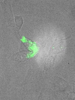
Image / Strano Laboratory, This image shows the cell before hydrogen peroxide is added.

carbon nanotubes to monitor chemotherapy

mage / Strano Laboratory, This image shows the cell after hydrogen peroxide is added. The change in fluorescence provides a "fingerprint" that allows different molecules to be identified.
Chemical engineers use carbon nanotubes to monitor chemotherapy, detect toxins at the single-molecule level

CAMBRIDGE, Mass.--MIT engineers have developed carbon nanotubes into sensors for cancer drugs and other DNA-damaging agents inside living cells.

The sensors, made of carbon nanotubes wrapped in DNA, can detect chemotherapy drugs such as cisplatin as well as environmental toxins and free radicals that damage DNA.

"We've made a sensor that can be placed in living cells, healthy or malignant, and actually detect several different classes of molecules that damage DNA," said Michael Strano, associate professor of chemical engineering and senior author of a paper on the work appearing in the Dec. 14 online edition of Nature Nanotechnology.

Such sensors could be used to monitor chemotherapy patients to ensure the drugs are effectively battling tumors. Many chemotherapy drugs are very powerful DNA disruptors and can cause serious side effects, so it is important to make sure that the drugs are reaching their intended targets.

"You could figure out not only where the drugs are, but whether a drug is active or not," said Daniel Heller, a graduate student in chemical engineering and lead author of the paper.

The sensor can detect DNA-alkylating agents, a class that includes cisplatin, and oxidizing agents such as hydrogen peroxide and hydroxyl radicals.
Using the sensors, researchers can monitor living cells over an extended period of time. The sensor can pinpoint the exact location of molecules inside cells, and for one agent, hydrogen peroxide, it can detect a single molecule.

The new technology takes advantage of the fact that carbon nanotubes fluoresce in near-infrared light. Human tissue does not, which makes it easier to see the nanotubes light up.

Each nanotube is coated with DNA, which binds to DNA-damaging agents present in the cell. That interaction between the DNA and DNA disruptor changes the intensity and/or wavelength of the fluorescent light emitted by the nanotube. The agents produce different signatures that can be used to identify them.

"We can differentiate between different types of molecules depending on how they interact," Strano said.

Because they are coated in DNA, these nanotube sensors are safe for injection in living cells. (Nanotubes can come in many different lengths and can be coated with different materials, which influences whether they are safe or toxic, Strano said.)

In future studies, the researchers plan to use the sensors to study the effects of various antioxidants, such as the compounds in green tea, and learn how to more effectively use toxic chemotherapy drugs. ###

Other authors of the paper include MIT graduate student Hong Jin of the Department of Chemical Engineering. Researchers from the University of Illinois at Urbana-Champaign also contributed to the work, which was funded by the National Science Foundation.

Contact: Elizabeth Thomson thomson@mit.edu 617-258-5402 Massachusetts Institute of Technology

Sunday, January 25, 2009

Method Sorts Out Double-Walled Carbon Nanotube Problem VIDEO

Mark Hersam

Mark Hersam
It's hard to study something with any rigor if the subject can't be produced uniformly and efficiently. Researchers who study double-walled carbon nanotubes -- nanomaterials with promising technological applications -- find themselves in just this predicament.

Interview with Mark C. Hersam of Northwestern University.
The problem is that current techniques for synthesizing double-walled carbon nanotubes also produce unwanted single- and multi-walled nanotubes. These two forms each have interesting properties, but an intriguing blend of those properties is found in double-walled nanotubes, attracting the attention of an increasing number of researchers. (A double-walled nanotube is made up of two concentric single-walled nanotubes.)

Perhaps most significantly, double-walled nanotubes provide distinct advantages when used in transparent conductors, materials that are important components of solar cells and flat-panel displays because they are optically transparent and electrically conductive. As the demand for energy-efficient devices and alternative energy sources rises worldwide so does the demand for transparent conductive films.
Two Northwestern University researchers now offer a clever solution to the double-walled nanotube production problem. They used a technique developed at Northwestern called density gradient ultracentrifugation to cleanly and easily separate the double-walled nanotubes (DWNTs) from the single-walled nanotubes (SWNTs) and multi-walled nanotubes (MWNTs). double-walled nanotube

Two single-walled nanotubes and a double-walled nanotube
The sorting method works by exploiting subtle differences in the buoyant densities of the nanotubes as a function of their size and electronic behavior. The results will be published online Sunday, Dec. 14, by the journal Nature Nanotechnology. The paper also will appear as the cover story in the January 2009 issue of the journal.

"Nanomaterials possess the unique attribute that their properties depend on physical dimensions such as diameter," said Mark C. Hersam, professor of materials science and engineering in Northwestern's McCormick School of Engineering and Applied Science, professor of chemistry in the Weinberg College of Arts and Sciences and the paper's senior author.

"This size dependence implies, however, that the physical dimensions must be exquisitely controlled in order to realize uniform and reproducible performance in devices. Our study directly addresses this issue for double-walled carbon nanotubes, an emerging nanomaterial with applications in information technology, biotechnology and alternative energy," said Hersam.

He collaborated with Alexander A. Green, a graduate student in materials science and engineering at Northwestern and lead author of the paper, titled "Processing and Properties of Highly Enriched Double-Walled Carbon Nanotubes."

Using the Northwestern method, carbon nanotubes first are encapsulated in water by soap-like molecules called surfactants. The surfactant-coated nanotubes then are sorted in density gradients that are spun at tens of thousands of rotations per minute in an ultracentrifuge. Each nanotube's diameter and electronic structure help determine the nanotube's buoyant density, which enables the method to separate DWNTs from the SWNTs and MWNTs.

The double-walled nanotubes, the researchers discovered, were approximately 44 percent longer than the single-walled nanotubes. This longer length of the DWNTs results in a factor of 2.4 improvement in the electrical conductivity of transparent conductors.

Double-walled nanotubes also enable improved spatial resolution and longer scanning lifetimes as tips for atomic force microscopes and are useful in field-effect transistors, biosensing and drug delivery.

The work was supported by the U.S. Army Telemedicine and Advanced Technology Research Center and the National Science Foundation.

Contact: Megan Fellman fellman@northwestern.edu 847-491-3115 Northwestern University

Saturday, January 24, 2009

Oregon theory may help design tomorrow's sustainable polymer

Marina Guenza, University of Oregon

Caption: Marina Guenza, a theoretical chemist at the University of Oregon, may have provided the why behind years of unexplained polymer data.

Credit: Photo by Jim Barlow. Usage Restrictions: None.
Theoretical chemist provides focus to years of unexplained behavior of molecules moving in plastics.

Tomorrow's specialty plastics may be produced more precisely and cheaply thanks to the apparently tight merger of a theory by a University of Oregon chemist and years of unexplained data from real world experiments involving polymers in Europe.
The work, which researchers believe may lead to a new class of materials, is described in a paper appearing in the Dec. 18 issue of the Journal of Physical Chemistry B (online Dec. 11). The findings eventually could prove useful in the fields of engineering, nanotechnology, renewable energy and, potentially, medicine, because proteins, DNA, RNA and other large molecules within cells may well move in the same way as those in plastics.

Traditional theory behind the processing of plastic materials since the 1960s has focused on the movement of individual macromolecules as they move by one another. Materials researchers, under this approach, end up with poorly understood products and unexplained data. The new theory of cooperative motion in liquids of polymers successfully explains these observations by considering the coordinated motion of macromolecules with their surrounding neighbors. The end result could remove guesswork and the costly, time-consuming testing of thousands of samples at various stages of production.

"The level of agreement between the data and the theory is remarkable," said Marina G. Guenza, a professor of theoretical physical chemistry at the UO. "We are making the connection between the chemistry of molecules and how they behave. It is really fundamental science. Our findings are exciting for experimentalists because we can see phenomena that they cannot understand. This theory is now explaining what is happening inside their samples. They are no longer dealing with just a set of data; our theory provides a picture of what is happening."

Guenza simplifies her mathematics-heavy theory -- built on Langevin equations that describe the movement of particles in liquid or gas -- to watching students disembark from a crowded bus. Any one student wanting to exit is stuck in place -- or meanders randomly in available spaces -- until other students begin moving toward the exit. As students organize into a group they become coordinated and speed their departure.

The theory addresses the often-seen subdiffusive behavior of molecules as they begin to form a glass under processing -- explaining why molecules slow and freeze into disorganized structures rather than ordering into a crystal, Guenza said. "We would really like to be able to control the properties of the material so that we can tailor the synthesis to achieve exact results."

The theory was put to the test under a variety of scenarios in labs in Germany, France and Switzerland after German plastics researcher Dieter Richter of the Max Planck Institute for Solid State Research, a co-author on the paper, approached Guenza after a conference session and said he had unexplained data that might be explained by Guenza's theory. The unexplained data and Guenza's theory merged under examination, which included the use of neutron spin-echo spectroscopy, a high-energy resolution-scattering technique.

"If you look at just one polymer, as is the case under conventional theory, you don't see any anomalous motion," said Guenza, whose research is funded by the National Science Foundation and the Petroleum Research Fund. "You don't see slowing one molecule alternating between slow and fast motion. Only if you treat the dynamics of a group of molecules together can you predict anomalous behaviors. That's what my theory can give you."

The theory now is being applied to other experiments to test its application to other anomalies, said Guenza, who is a member of three UO interdisciplinary institutes: the Institute of Theoretical Science; the Materials Science Institute and the Institute of Molecular Biology. ###

Co-authors of the paper with Guenza and Richter were Richter's colleagues M. Zamponi, A. Wischnewski, M. Monkenbusch and L. Willner, and researchers P. Falus and B. Farago, both of the Institut Laue-Langevin, a leading international neutron research center in Grenoble, France.

About the University of Oregon

The University of Oregon is a world-class teaching and research institution and Oregon's flagship public university. The UO is a member of the Association of American Universities (AAU), an organization made up of 62 of the leading public and private research institutions in the U.S. and Canada. The University of Oregon is one of only two AAU members in the Pacific Northwest.

Source: Marina Guenza, associate professor, department of chemistry, 541-346-2877, mguenza@uoregon.edu

Links: Contact: Jim Barlow jebarlow@uoregon.edu 541-346-3481 University of Oregon

Friday, January 23, 2009

People in the US and the UK show strong similarities in their attitudes toward nanotechnologies

Barbara Herr Harthorn

Barbara Herr Harthorn Professor. 4713 South Hall. University of California, Santa Barbara, CA 93106-7110, Phone: 805-893-3350, Fax: 805-893-8676. e-mail: herrharthorn@femst.ucsb.edu
(Santa Barbara, Calif.) –– The results of a new U.S.–U.K. study published in this week's journal Nature Nanotechnology show that ordinary people in both countries hold very positive views of nanotechnologies and what the future of these technologies might bring. Participants in both countries indicated a significantly higher comfort level with energy applications of nanotechnologies than with applications used in health treatments.

Nanotechnology –– the science and technology of exceptionally small materials and processes –– is among the latest new technologies to raise public concerns about health and environmental risks.
The article reports on the first study of its kind. It involved four workshops, held at the same time in Santa Barbara and Cardiff, Wales. Workshop participants deliberated about two broad types of nanotechnology applications –– energy and health.

The study was carried out in the United States by the NSF Center for Nanotechnology in Society at the University of California, Santa Barbara, and in the United Kingdom by a collaborating research team from the School of Psychology at Cardiff University.

Barbara Herr Harthorn, director of the UCSB Center, led the interdisciplinary, international research team. She noted that one of the unexpectedly strong findings of the study was that the type of nanotechnology mattered greatly to the participants. She said participants in both countries viewed energy applications of nanotechnology more positively than health technologies, in terms of risks and benefits.

"Much of the public perception research on nanotechnology in the U.S. and abroad has focused on a generic 'nanotechnology' risk object," said Harthorn. "This work moves to a higher level of specificity and in doing so finds striking differences in views of benefit depending on application context.

"More specifically, perceived urgency of need for new energy technologies is strongly associated with high perceived benefit and lower risk perception, regardless of what materials, processes, or environmental risks are associated," she said.

Nick Pidgeon, who led the research team at the School of Psychology at Cardiff University, explained, "The Royal Society's 2004 report on nanotechnologies recommended public engagement and deliberation on nanotechnology risks and benefits. This study represents the first ever such public engagement exercise to be simultaneously conducted in two different countries."

The results include the following key findings:

* Overall participants in both countries focused on the benefits rather than the risks of nanotechnologies, and also exhibited a high degree of optimism regarding the future contribution of new technologies to society. This pattern was very similar in the workshops in both the United States and Britain.

* Some small cross-country differences were present. U.K. participants were generally more aware of recent technological controversies and risk governance failures (examples include genetically modified organisms, bovine spongiform encephalopathy (BSE), and foot and mouth disease), leading some to voice specific concerns about future nanotechnology risks.

* Greater differences were observed when participants (irrespective of their country) discussed the different applications. In particular, new technology developments for energy applications were seen as unproblematic, while questions of human health were felt to raise moral and ethical dilemmas. As was found by the U.K. Royal Society in 2004 for Britain, in the current study participants in both the U.K. and U.S. questioned whether those responsible (governments, industry, scientists) could be fully trusted to control nanotechnologies in the future. ###

The research was funded primarily by the National Science Foundation with additional support to Cardiff University provided by the Leverhulme Trust.

The NSF Center for Nanotechnology in Society at UCSB (www.cns.ucsb.edu) was formed in 2006, and serves as a national research and education center, a network hub among researchers and educators concerned with societal issues and nanotechnologies, and a resource base for studying these issues.

Contact: Gail Gallessich gail.g@ia.ucsb.edu 805-893-7220 University of California - Santa Barbara

Thursday, January 22, 2009

NPL research shows there could be no end in sight for Moore’s Law

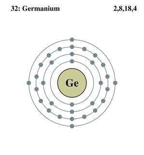
Germanium, the 32nd element

Electron shell diagram for Germanium, the 32nd element in the periodic table of elements.
The fast pace of growing computing power could be sustained for many years to come thanks to new research from the UK's National Physical Laboratory (NPL) that is applying advanced techniques to magnetic semiconductors. Moore's Law observed that the density of transistors on an integrated circuit doubles every two years.
Components have shrunk over time to achieve this, but experts believed that when the characteristic transistor size reduces below ~ 20 nm, heating and quantum effects will become so severe that they will not be of practical use.

In a paper published in one of the most cited scientific journals, Nano Letters (ISI citation factor is 9.627), researchers at NPL looked at solutions to this problem as part of a project dealing with magnetic phenomena at reduced dimensions.

In the paper NPL's scientists reported on their research on single crystalline Mn-doped Ge nanowires that display ferromagnetism above 300 K and a superior performance with respect to the hole mobility of around 340 cm2/Vs and other industrially relevant parameters, demonstrating the potential of using these nanowires as building blocks for electronic devices.

Senior Research Scientist at NPL Dr Olga Kazakova said:

'The solution lies in changing not only the material but also the structure of our transistors. We have worked mainly with germanium nanowires that we have made magnetic. Magnetic semiconductors don't exist in nature, so they have to be artificially engineered. Germanium is closely compatible with silicon, meaning it can easily be used with existing silicon electronics without further redesign. The resulting transistors based on NPL's germanium nanowire technology, which could revolutionise computing and electronic devices, could realistically be 10 years away." ###

The work is a result of close collaboration between scientists in Ireland (UCC and Trinity College), USA (Intel Corporation and Univ. of California) and the UK (NPL).

Notes to Editors, About The National Physical Laboratory (NPL)

The National Physical Laboratory (NPL) is one of the UK's leading science facilities and research centres. It is a world-leading centre of excellence in developing and applying the most accurate standards, science and technology available.

NPL occupies a unique position as the UK's National Measurement Institute and sits at the intersection between scientific discovery and real world application. Its expertise and original research have underpinned quality of life, innovation and competitiveness for UK citizens and business for more than a century:

NPL provides companies with access to world leading support and technical expertise, inspiring the absolute confidence required to realise competitive advantage from new materials, techniques and technologies

NPL expertise and services are crucial in a wide range of social applications - helping to save lives, protect the environment and enable citizens to feel safe and secure. Support in areas such as the development of advanced medical treatments and environmental monitoring helps secure a better quality of life for all

NPL develops and maintains the nation's primary measurement standards, supporting an infrastructure of traceable measurement throughout the UK and the world, to ensure accuracy and consistency.

Contact: Joe Meaney joe@proofcommunication.com 084-568-01864 National Physical Laboratory

Wednesday, January 21, 2009

New hybrid nanostructures detect nanoscale magnetism

New Hybrid Nanostructure

Caption: Pictured is a rendering depicting cobalt nanoclusters embedded in multi-walled carbon nanotubes. Credit: Image credit: Saikat Talapatra/Caterina Soldano. Usage Restrictions: Please include photo credit.
Research could pave way for new data storage devices, drug delivery systems.

Troy, N.Y. – A key challenge of nanotechnology research is investigating how different materials behave at lengths of merely one-billionth of a meter. When shrunk to such tiny sizes, many everyday materials exhibit interesting and potentially beneficial new properties.
Magnetic behavior is one such phenomenon that can change significantly depending on the size of the material. However, the sheer challenge of observing the magnetic properties of nanoscale material has impeded further study of the topic.

Researchers at Rensselaer Polytechnic Institute have developed and demonstrated a new method for detecting the magnetic behaviors of nanomaterials. They created a new process for growing a single multi-walled carbon nanotube that is embedded with cobalt nanostructures. The cobalt clusters measure from 1 nanometer to 10 nanometers.
After a series of experiments, the research team has concluded that the electrical conductance of carbon nanotubes is sensitive enough to detect and be affected by trace amounts of magnetic activity, such as those present in the embedded cobalt nanostructures. It is believed to be the first instance of demonstrating the detection of magnetic fields of such small magnets using an individual carbon nanotube.

Results of the study were reported in the paper "Detection of Nanoscale Magnetic Activity Using a Single Carbon Nanotube" recently published by Nano Letters.
New Hybrid Nanostructure

Caption: Pictured is a scanning electron micrograph of cobalt nanoclusters embedded in multi-walled carbon nanotubes. Researchers at Rensselaer used these new hybrid structures, the first of their kind, to detect magnetism at the nanoscale.

Credit: Image credit: Saikat Talapatra/Caterina Soldano. Usage Restrictions: Please include photo credit.
"Since the cobalt clusters in our system are embedded inside the nanotube rather than on the surface, they do not cause electron scattering and thus do not seem to impact the attractive conductive properties of the host carbon nanotube," said Swastik Kar, research assistant professor in Rensselaer's Department of Physics, Applied Physics, & Astronomy, who led the project. "From a fundamental point of view, these hybrid nanostructures belong to a new class of magnetic materials."

"These novel hybrid nanostructures open up new avenues of research in fundamental and applied physics, and pave the way for increased functionality in carbon nanotube electronics utilizing the magnetic degree of freedom that could give rise to important spintronics applications," said Saroj Nayak, an associate professor in Rensselaer's Department of Department of Physics, Applied Physics, and Astronomy, who also contributed to the project.

Potential applications for such a material include new generations of nanoscale conductance sensors, along with new advances in digital storage devices, spintronics, and selective drug delivery components. ###

Co-authors of the paper include Caterina Soldano, formerly a graduate student at Rensselaer who is now a postdoctoral research associate at the Centre d'Elaboration de Matériaux et d'Etudes Structurales in Tolouse, France; Professor Saikat Talapatra of the Physics Department of Southern Illinois University, Carbondale; and Prof. P.M. Ajayan of the Rice University Department of Mechanical Engineering and Materials Science.

Researchers received funding for the project from the New York State Interconnect Focus Center at Rensselaer.

Contact: Michael Mullaney mullam@rpi.edu 518-276-6161 Rensselaer Polytechnic Institute

Tuesday, January 20, 2009

"Strained" Quantum Dots Show New Optical Properties

Strained Quantum DotsQuantum dots, tiny luminescent particles made of semiconductors, hold promise for detecting and treating cancer earlier.
However, if doctors were to use them in humans, quantum dots could have limitations related to their size and possible toxicity.

Scientists at Emory University and the Georgia Institute of Technology have found a way around those limitations by exploiting a property of semiconductors called "lattice strain." By layering materials with different chemical compositions on top of each other, the researchers can create particles with new optical properties.

A description of the "strain-tuned" particles is available online this week and is scheduled for publication in the December issue of the journal Nature Nanotechnology.

"The first generation of quantum dots had optical properties that could be tuned by their size," says senior author Shuming Nie, PhD, a professor in the Wallace H. Coulter Department of Biomedical Engineering at Georgia Tech and Emory University. "We have discovered another way to tune quantum dots' properties-- by modulating lattice strain."

In addition to their expected utility in biomedical imaging, the new type of quantum dots could find use in optoelectronics, advanced color displays and more efficient solar panels, Nie adds.

A mismatch between the lattices of the semiconductors making up the inner core and outside shell of the particle creates strain: the core is squeezed and the shell is stretched. This physical strain changes the energies and wavelengths of the light produced by the quantum dot.

Previous quantum dots contained cadmium, a toxic heavy metal. Strain-tuned quantum dots can be made mostly of the less toxic elements zinc and selenium, although some cadmium remains at the core of the particle. The particles can be between four and six nanometers wide.

Adding layers of zinc and selenium on top of a cadmium and tellurium core increases the wavelength of light produced as fluorescence by the quantum dots, Nie's team shows. As the core becomes smaller, the shift in the fluorescence wavelength produced by the zinc-containing layers becomes larger.

Strain-tuned quantum dots can be made that emit light at wavelengths in the near-infrared range while remaining small in size. Near-infrared wavelengths around 750 nanometers represent a "clear window" where the human body is relatively transparent, says Andrew Smith, PhD, a postdoctoral fellow in Nie's group and the first author of the paper.

While the newer strain-tuned quantum dots have not been tested in living animals or people, they could probably pass through the kidneys, meaning less toxicity, if they are less than five nanometers in diameter, Smith remarks.

"Using near-infrared wavelengths, there's less difficulty in seeing through the body's tissues," he continues. "Older quantum dots that emit in the near-infrared range are rod-shaped and large enough to get trapped in the kidneys, while smaller particles can both clear the kidneys and have less of a tendency to bind proteins in the blood."

"Core-shell nanocrystals are all expected to have some lattice mismatch between the core and the shell, so the strain effect is a general phenomenon," Nie says. "But this effect was not well understood in the past, and was often not taken into consideration. Our work shows that lattice strain is another key factor that must be considered, in addition to particle size and composition."

The National Institutes of Health, the Department of Energy and the Georgia Cancer Coalition funded the research.

Reference: Smith, A.M., Mohs, A.M and Nie, S. Tuning the optical and electronic properties of colloidal nanocrystals by lattice strain. Nature Nanotechnology, advance online publication, December 2008. ###

The Robert W. Woodruff Health Sciences Center of Emory University is an academic health science and service center focused on missions of teaching, research, and health care. Its components include schools of medicine, nursing, and public health; the Yerkes National Primate Research Center; the Emory Winship Cancer Institute; and Emory Healthcare, the largest, most comprehensive health system in Georgia. The Health Sciences Center has a $2.3 billion budget, 17,000 employees, 2,300 full-time and 1,900 affiliated faculty, 4,300 students and trainees, and a $4.9 billion economic impact on metro Atlanta.

Contact: Holly Korschun hkorsch@emory.edu 404-727-3990 Emory University

Monday, January 19, 2009

Nanotechnology 'culture war' possible, says Yale study

Nanowire Lasers

Caption: Nanowire lasers are one new development of nanotechnology. Credit: Nicolle Rager Fuller, National Science Foundation. Usage Restrictions: None.
New Haven, Conn, — Rather than infer that nanotechnology is safe, members of the public who learn about this novel science tend to become sharply polarized along cultural lines, according to a study conducted by the Cultural Cognition Project at Yale Law School in collaboration with the Project on Emerging Nanotechnologies. The report is published online in the journal Nature Nanotechnology.
These findings have important implications for garnering support of the new technology, say the researchers.

The experiment involved a diverse sample of 1,500 Americans, the vast majority of whom were unfamiliar with nanotechnology, a relatively new science that involves the manipulation of particles the size of atoms and that has numerous commercial applications. When shown balanced information about the risks and benefits of nanotechnology, study participants became highly divided on its safety compared to a group not shown such information.

The determining factor in how people responded was their cultural values, according to Dan Kahan, the Elizabeth K. Dollard Professor at Yale Law School and lead author of the study. "People who had more individualistic, pro-commerce values, tended to infer that nanotechnology is safe," said Kahan, "while people who are more worried about economic inequality read the same information as implying that nanotechnology is likely to be dangerous."

According to Kahan, this pattern is consistent with studies examining how people's cultural values influence their perceptions of environmental and technological risks generally. "In sum, when they learned about a new technology, people formed reactions to it that matched their views of risks like climate change and nuclear waste disposal," he said.

The study also found that people who have pro-commerce cultural values are more likely to know about nanotechnology than others. "Not surprisingly, people who like technology and believe it isn't bad for the environment tend to learn about new technologies before other people do," said Kahan. "While various opinion polls suggest that familiarity with nanotechnology leads people to believe it is safe, they have been confusing cause with effect."

According to Kahan and other experts, the findings of the experiment highlight the need for public education strategies that consider citizens' predispositions. "There is still plenty of time to develop risk-communication strategies that make it possible for persons of diverse values to understand the best evidence scientists develop on nanotechnology's risks," added Kahan. "The only mistake would be to assume that such strategies aren't necessary."

"The message matters," said David Rejeski, director of the Project on Emerging Nanotechnologies. "How information about nanotechnology is presented to the vast majority of the public who still know little about it can either make or break this technology. Scientists, the government, and industry generally take a simplistic, 'just the facts' approach to communicating with the public about a new technology. But, this research shows that diverse audiences and groups react to the same information very differently." ###

The study was supported by the National Science Foundation, the Oscar M. Ruebhausen Fund at Yale Law School, and the Project on Emerging Nanotechnologies.

The Cultural Cognition Project at Yale Law School is an interdisciplinary team of scholars from Yale University, the University of Washington, George Washington University, the University of Colorado, and Decision Research. The project studies how people's values affect their views on various societal risks, including climate change, gun ownership, and nanotechnology, among others. For more information, visit www.culturalcognition.net.

The Project on Emerging Nanotechnologies is an initiative launched by the Woodrow Wilson International Center for Scholars and The Pew Charitable Trusts in 2005. It is dedicated to helping business, government and the public anticipate and manage possible health and environmental implications of nanotechnology. For more information about the project, log on to www.nanotechproject.org.

About nanotechnology: Nanotechnology is the ability to measure, see, manipulate and manufacture things usually on a scale between 1 and 100 nanometers. A nanometer is one billionth of a meter; a human hair is roughly 100,000 nanometers wide. In 2007, the global market for goods incorporating nanotechnology totaled $147 billion. Lux Research projects that figure will grow to $3.1 trillion by 2015.

Citation: Nature Nanotechnology (Advance Online Publication December 7, 2008)
doi: 10.1038/NNANO.2008.341

Dan Kahan www.law.yale.edu/faculty/DKahan

Contact: Janet Rettig Emanuel janet.emanuel@yale.edu 203-432-2157 Yale University

Sunday, January 18, 2009

For nano, religion in US dictates a wary view

nanotechnology was morally acceptable

The average responses plotted here somewhat underrepresent the range of responses across all response categories. The proportion of respondents who disagree (i.e., -1 or -2) that nanotechnology was morally acceptable was highest in the U.S. (24.9 percent) and lowest in Italy (7.3 percent). The percentages for respondents who agree (i.e., +1 or +2) was highest in Belgium (82.4 percent) and lowest in Ireland (33.5 percent).
MADISON — When it comes to the world of the very, very small — nanotechnology — Americans have a big problem: Nano and its capacity to alter the fundamentals of nature, it seems, are failing the moral litmus test of religion.

In a report published today (Dec. 7) in the journal Nature Nanotechnology, survey results from the United States and Europe reveal a sharp contrast in the perception that nanotechnology is morally acceptable.
Those views, according to the report, correlate directly with aggregate levels of religious views in each country surveyed.

In the United States and a few European countries where religion plays a larger role in everyday life, notably Italy, Austria and Ireland, nanotechnology and its potential to alter living organisms or even inspire synthetic life is perceived as less morally acceptable. In more secular European societies, such as those in France and Germany, individuals are much less likely to view nanotechnology through the prism of religion and find it ethically suspect.

"The level of 'religiosity' in a particular country is one of the strongest predictors of whether or not people see nanotechnology as morally acceptable," says Dietram Scheufele, a UW-Madison professor of life sciences communication and the lead author of the new study. "Religion was the strongest influence over everything."

The study compared answers to identical questions posed by the 2006 Eurobarometer public opinion survey and a 2007 poll by the University of Wisconsin Survey Center conducted under the auspices of the National Science Foundation-funded Center for Nanotechnology and Society at Arizona State University. The survey was led by Scheufele and Elizabeth Corley, an associate professor in the School of Public Affairs at Arizona State University.

The survey findings, says Scheufele, are important not only because they reveal the paradox of citizens of one of the world's elite technological societies taking a dim view of the implications of a particular technology, but also because they begin to expose broader negative public attitudes toward science when people filter their views through religion.

"What we captured is nanospecific, but it is also representative of a larger attitude toward science and technology," Scheufele says. "It raises a big question: What's really going on in our public discourse where science and religion often clash?"

For the United States, the findings are particularly surprising, Scheufele notes, as the country is without question a highly technological society and many of the discoveries that underpin nanotechnology emanated from American universities and companies. The technology is also becoming more pervasive, with more than 1,000 products ranging from more efficient solar panels and scratch-resistant automobile paint to souped-up golf clubs already on the market.

"It's estimated that nanotechnology will be a $3.1 trillion global industry by 2015," Scheufele says. "Nanotechnology is one of those areas that is starting to touch nearly every part of our lives."

To be sure that religion was such a dominant influence on perceptions of nanotechnology, the group controlled for such things as science literacy, educational performance, and levels of research productivity and funding directed to science and technology by different countries.

"We really tried to control for country-specific factors," Scheufele explains. "But we found that religion is still one of the strongest predictors of whether or not nanotechnology is morally acceptable and whether or not it is perceived to be useful for society."

The findings from the 2007 U.S. survey, adds Scheufele, also suggest that in the United States the public's knowledge of nanotechnology has been static since a similar 2004 survey. Scheufele points to a paucity of news media interest and the notion that people who already hold strong views on the technology are not necessarily seeking factual information about it.

"There is absolutely no change in what people know about nanotechnology between 2004 and 2007. This is partly due to the fact that mainstream media are only now beginning to pay closer attention to the issue. There has been a lot of elite discussion in Washington, D.C., but not a lot of public discussion. And nanotechnology has not had that catalytic moment, that key event that draws public attention to the issue." ###

Terry Devitt, 608-262-8282, trdevitt@wisc.edu

Contact: Dietram Scheufele scheufele@wisc.edu 608-262-1614 University of Wisconsin-Madison

Saturday, January 17, 2009

New holographic method could be used for lab-on-a-chip technologies VIDEO

Holographic Technique

Caption: These images were taken from a video illustrating a new technique that uses a laser and holograms to precisely position clusters of numerous tiny particles within seconds, representing a potential new tool to analyze biological samples or create devices using "nanoassembly." The red dots are individual particles.

Credit: Birck Nanotechnology Center, Purdue University, Usage Restrictions: None.
WEST LAFAYETTE, Ind. - VIDEO Optically induced electrokinetic patterning and manipulation of particles Researchers at Purdue University have developed a technique that uses a laser and holograms to precisely position numerous tiny particles within seconds, representing a potential new tool to analyze biological samples or create devices using nanoassembly.

The technique, called rapid electrokinetic patterning, is a potential alternative to existing technologies because the patterns can be more quickly and easily changed, said mechanical engineering doctoral student Stuart J. Williams.

"It's potentially a very versatile tool," said Williams, who is working with doctoral student Aloke Kumar and Steven T. Wereley, an associate professor of mechanical engineering.

The research is based at the Birck Nanotechnology Center in Purdue's Discovery Park.

The students won a research award for their work in October during the 12th International Conference on Miniaturized Systems for Chemistry and Life Sciences in San Diego.
Four young researcher poster awards were selected out of more than 220 posters judged in the contest. Findings also have been recently published in two peer-reviewed journals, Lab on a Chip and Microfluidics and Nanofluidics.

The experimental device consists of two parallel electrodes made of indium tin oxide, a transparent and electrically conductive material. The parallel plates were spaced 50 micrometers, or millionths of a meter, apart, equivalent to two-thousandths of an inch or about the diameter of a human hair. A liquid sample containing fluorescent beads was injected between the two electrodes, a laser in the near infrared range of the spectrum was shined through one of the transparent electrodes and a small electrical voltage was applied between the two electrodes.

"We send holograms of various patterns through this and, because they are holograms, we can create different shapes, such as straight lines or L patterns," Kumar said.

The particles in the liquid sample automatically move to the location of the light and assume the shape of the hologram, meaning the method could be used to not only move particles and molecules to specific locations but also to create tiny electronic or mechanical features.

"It's a very dynamic system, so we can change this pattern quickly," Kumar said.

The light heats up the liquid sample slightly, changing its density and electrical properties. The electric field applied to the plates acts on these altered properties, causing the heated sample to circulate, much like heated air causes convection currents in the atmosphere, producing a donut-shaped "microfluidic vortex" of circulating liquid between the two plates.

This vortex enables the researchers to position the particles in the circulating liquid by moving the laser light.

"You could take one particle, a hundred particles or a thousand particles and move them anywhere you want in any shape that you want," Williams said. "If you have particles of two different types, you can sort one group out and keep the other behind. It's a versatile tool."

Separating particles is important for analyzing medical and environmental samples. The system could allow researchers to design sensor technologies that move particles to specific regions on an electronic chip for detection or analysis.

The technique overcomes limitations inherent in two existing methods for manipulating particles measured on the scale of nanometers, or billionths of a meter. One of those techniques, called optical trapping, uses a highly focused beam of light to capture and precisely position particles. That technique, however, is able to move only a small number of particles at a time.

The other technique, known as dielectrophoresis, uses electric fields generated from metallic circuits to move many particles at a time. Those circuit patterns, however, cannot be changed once they are created.

The new method is able to simultaneously position numerous particles and be changed at a moment's notice simply by changing the shape of the hologram or the position of the light.

"If you want to pattern individual particles on a massive scale using electrokinetic methods as precisely as we are doing it, it could take hours to days, where we are doing it in seconds," Williams said.

The method offers promise for future "lab-on-a-chip" technology, or using electronic chips to analyze biological samples for medical and environmental applications. Researchers are trying to develop such chips that have a "high throughput," or the ability to quickly detect numerous particles or molecules, such as proteins, using the smallest sample possible.

"For example, a single drop of blood contains millions of red blood cells and countless molecules," Williams said. "You always want to have the smallest sample possible so you don't generate waste and you don't have to use as many chemicals for processing the sample. You want to have a very efficient high throughput type of device."

So-called "optical tweezers" use light to position objects such as cells or molecules.

"You can't use mechanical tweezers to move things like molecules because they are too delicate and will be damaged by conventional tweezers," Kumar said. "That is why techniques like optical tweezing and dielectrophoresis are very popular."

The students also have designed an experiment containing one indium tin oxide plate and one gold plate, an important development because gold is often used in biomedical applications.

"It's a technique that you would likely use in sensors, but we also see definite potential ways in which you could use it to manufacture devices with nanoassembly," Wereley said. "But it's really too soon to talk about scaling this up in a manufacturing setting. We're just beginning to develop this technique."

The researchers recorded videos of the circulating particles to document the effect. A video showing the effect was selected as an outstanding entry during a meeting of the American Physical Society in November. The video can be accessed at http://ecommons.cornell.edu/handle/1813/11399.

"This technique has not been done before," Williams said. "We can pattern light, we can pattern particles, we can pattern the vortex. No other tool can do all of these."

The researchers demonstrated how the method could be used to cause particles to stick permanently to a surface in a single crystalline layer, a structure that could be used in manufacturing. They used their technique to move fluorescent-dyed beads of polystyrene, latex and glass in sizes ranging from 50 nanometers to 3 micrometers.

Future work may involve using a less expensive light source, such as a common laser pointer, which could not be used to create intricate patterns but might be practical for manufacturing. ###

Kumar and Williams also won a first place Birck Nanotechnology Center award in April for the research. The work has been supported with funding from the National Science Foundation.

Writer: Emil Venere, (765) 494-4709, venere@purdue.edu

Sources:Related Web sites:Contact: Emil Venere venere@purdue.edu 765-494-4709 Purdue University

Friday, January 16, 2009

Ship-in-a-bottle kit on a microchip

Microspheres in a Magnetic Field

Caption: Pumps teaming up and working together: In a magnetic field the microspheres (orange) form diamond shaped valves and a cog wheel. With skilful manipulation of a magnetic field, the wheel rolls through the cavity, and together with the valves pumps a fluid with colloid particles (blue) through the system.

Credit: Sabri Rahmouni/University of Stuttgart. Usage Restrictions: None.
Sometimes physicists resort to tried and trusted model-making tricks. Scientists at the Max Planck Institute for Metals Research, the University of Stuttgart and the Colorado School of Mines have constructed micromachines using the same trick that model makers use to get ships into a bottle where the masts and rigging of the sailing ship are not erected until it is in the bottle. In the same way, the scientists link the valves, pumps and stirrers of a microlaboratory to create a micro device on a chip.
To do this, they introduce colloidal particles - tiny magnetizable plastic spheres - as components into the channels on the chip. A rotating magnetic field is used to link the components into larger aggregates and set them into motion as micromachines. (Proceedings of the National Academy of Sciences (PNAS), December 2, 2008)

In the future, biologists and chemists want to avoid using bulky glass flasks, Bunsen burners and magnetic stirrers as far as possible in their experiments. Similarly to microelectronics, where electrons are steered through tiny conducting paths, they intend to perform chemical reactions in microfluidic systems, that is, chambers and channels just a few micrometers in diameter. These "labs on a chip" will then allow DNA sequences or blood samples to be analyzed much more quickly and more efficiently. As they only require tiny amounts of liquids, this approach costs much less than traditional methods, which require larger quantities of materials. These micro analytical systems would also be transportable, because their core parts take up very little space. Paramedics, for example, could analyze blood samples at the site of an accident.

Researchers working with Clemens Bechinger who is a Professor at the University of Stuttgart and a Fellow at the Max Planck Institute for Metals Research, and David Marr, a professor at the Colorado School of Mines, have now found a new way to equip these miniaturized laboratories with moving parts and how to drive the tiny machines. They introduce colloidal particles, tiny plastic spheres with a diameter of just about five micrometers, into the channels and cavities on the chip.

As the particles contain iron oxide, they group together when they are magnetized by an external magnetic field. The scientists construct the magnetic field with four coils so that the microparticles are literally remote controlled and form diamond shapes or cog wheels. "The shape they assemble into depends crucially on the geometry of the channels," explains Tobias Sawetzki, who a doctoral student is working on the project. The microparticles then remain in this shape as long as the magnetic field is switched on.

The geometry also determines the function of the aggregates. By tipping backwards and forwards, a rhombus creates openings and acts like a valve. On the other hand, if it rotates in a chamber with two inflows, it mixes the incoming liquids. The micro stirrer is also driven by a magnetic field that rotates clockwise or anticlockwise parallel to the chip. In the same way, the researchers in Stuttgart roll a cog wheel through a channel with a serrated wall. The cog wheel, which completely shuts the channel off, agitates liquid back and forth and only in combination with two valves, acts like a pump.

"Compared to other approaches to equipping microlaboratories with moving parts, our ship-in-a-bottle technique has several advantages," says David Marr. Some scientists use pneumatic systems to pump liquids through microchannels, for example. However, this requires each component to be connected with a separate hose to the outside so that it can be supplied with compressed air. This is very complex and limits the integration density on microfluidic devices considerably, i.e. the total number of components on the chip.

With the new method, it is possible to accommodate up to 5,000 pumps on one square centimetre. Moreover, the new approach does not rely on elastic materials as are required for pneumatic pumps. "It is much easier to produce suitable chips for applications if they only consist of a single material, silicon, if at all possible," says Clemens Bechinger. As the electrical control components like the mini-coils can be fabricated based on silicon, it would be ideal to make the microchannels from the same material. This would allow for integration of all the components on one chip, as in microelectronics," says Bechinger.

Currently the researchers are still using large coils, so that all the components are driven by a single magnetic field and they all move in time with each other. However, this need not be a disadvantage as processes in many applications run in parallel; for example when the pharmaceutical industry searches for a new active ingredient amongst many thousands of substances. Furthermore, the researchers can choose the geometry of the channels so skilfully that different aggregates fulfil completely different functions in the same magnetic field. This means that the Stuttgart physicists' method offers the option of driving a complex network of individual, standalone components with only one magnetic field. ###

Original work:
  • Tobias Sawetzki, Sabri Rahmouni, Clemens Bechinger, David W.M. Marr
  • In-Situ Assembly of Linked Geometrically-Coupled Microdevices
  • Proceedings of the National Academy of Sciences (PNAS), December 2, 2008
Contact: Clemens Bechinger: c.bechinger@physik.uni-stuttgart.de 49-711-685-65218. Max-Planck-Gesellschaft

Thursday, January 15, 2009

Stanford blood scanner detects even faint indicators of cancer

" id="BLOGGER_PHOTO_ID_5291650074890931618" border="0">

Caption: Researchers led by Stanford professor Shan Wang have built a handheld device that finds event faint signs of cancer in a blood sample.

Credit: Sebastian Osterfeld, Stanford University. Usage Restrictions: None.
A team led by Stanford researchers has developed a prototype blood scanner that can find cancer markers in the bloodstream in early stages of the disease, potentially allowing for earlier treatment and dramatically improved chances of survival.

The system based on MagArray biodetection chips can find cancer-associated proteins in a blood serum sample in less than an hour, and with much greater sensitivity than existing commercial devices.
In fact, the device, which uses magnetic nanotechnology to spot the cancer proteins, is tens to hundreds of times more sensitive, meaning the proteins can be found while there are relatively few of them in the bloodstream. The researchers reported their results in the Dec. 1 online edition of the Proceedings of the National Academy of Sciences (PNAS).

"This is essentially a proof-of-concept study showing that now we have a chip and a reader that can find multiple biomarkers in a sample at a concentration much lower than the standard that is commercially available," said Shan Wang, a Stanford professor of materials science and of electrical engineering.

Wang is optimistic that the technology will someday save lives by detecting cancer early or by helping doctors select more effective therapy. "The earlier you can detect a cancer, the better chance you have to kill it," he said. "This could be especially helpful for lung cancer, ovarian cancer and pancreatic cancer, because those cancers are hidden in the body."

Wang is a senior author of the paper, along with Stanford biochemistry and genetics Professor Ronald W. Davis of the Stanford Genome Technology Center, and UC Santa Cruz biomolecular engineering Professor Nader Pourmand.

The detector is able to detect many different kinds of proteins at the same time, which is important for two reasons, Wang said. First, researchers are still uncertain which cancer biomarkers are the best diagnostic indicators. Secondly, detecting multiple biomarkers simultaneously will allow a doctor to diagnose more specifically the kind of cancer a patient may have.

Wang says the handheld device could be the smallest protein array reader in the world.

By means of magnets

The specialty of Wang's research group at Stanford is magnetic nanotechnology. Magnetism is rare in biological systems, so any magnetic signal in a blood serum sample stands out like a flare in the night sky. By tagging cancer proteins with tiny magnetic particles, rather than electrically charged or glowing particles as in other detectors, the new system can obtain a clearer signal from a smaller number of cancer proteins.

At the heart of the detector is a silicon chip, designed by the paper's lead author, Sebastian Osterfeld, a Stanford materials science and engineering doctoral student. The chips have 64 embedded sensors that monitor for changes in nearby magnetic fields. Attached to these sensors are "capture antibodies," painstakingly selected by Heng Yu, formerly a postdoctoral fellow at Stanford Genome Technology Center, and Richard Gaster, a student in a combined program of doctorate and medical degrees.

The sensor's "capture antibodies" grab specific cancer-related proteins as they float by and hold onto them. Then a second batch of antibodies is added to the mix. They latch onto magnetic nanoparticles as well as the cancer biomarkers that are being held captive by the sensors. Thus when the MagArray sensors detect the magnetic field of nanoparticles, they've found cancer markers as well.

In the paper, the researchers estimate that they could detect levels of the human chorionic gonadotropin protein at a level about 400 times lower than the level required for detection by current commercial kits known by the acronym ELISA, in which captured cancer proteins are tethered to color altering or fluorescent labels. At Stanford Medical Center, the detector is viewed as a potentially significant clinical advance, according to a diagnostics expert there.

"This work represents a giant leap forward in enabling technology for in vitro protein diagnostics with significant potential for many applications including cancer detection and management," said Dr. Sam Gambhir, the principal investigator of the Center of Cancer Nanotechnology Excellence at Stanford.

Headed for hospitals?

To properly prepare a patient's blood sample for use with the detector, a technician must use a centrifuge to separate out the serum, which contains the biomarkers. For this reason, the device must be located in a hospital or a private diagnostic lab, Wang said. But before then it must face clinical testing and trials to win regulatory approval. To see the detector through those steps, Wang has co-founded a startup company, MagArray Inc., in the Panorama Institute for Molecular Medicine, a not-for-profit incubator in Sunnyvale, Calif.

The nascent startup is also investigating the possible use of the detectors in emergency rooms to quickly check for heart attacks when patients arrive with chest pains. Like cancer, heart cell death is associated with the release of specific biomarker proteins. ###

The research was funded partly by grants from the U.S. National Institutes of Health, the National Science Foundation, and the Department of Defense. Other authors on the paper include Stefano Caramuta, Liang Xu, Shu-Jen Han, Drew Hall, Robert Wilson and Robert White, all of Stanford, and Shouheng Sun, of Brown University.

David Orenstein is the communications and PR manager for the Stanford School of Engineering.

RELEVANT WEB URLS: Contact: David Orenstein davidjo@stanford.edu 650-736-2245 Stanford University