Sunday, August 31, 2008

Golden scales

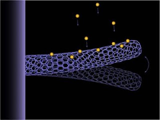
NEMS Mass Sensor

Caption: A double-walled carbon nanotube NEMS has been used to measure the mass of a single atom of gold. Atoms landing on the tube change the tube's resonant frequency in proportion to the mass of the atoms, much like what happens when a diver hits a springboard.

Credit: image by Kenneth Jensen. Usage Restrictions: None.
Nanoscale mass sensor from Berkeley can be used to weigh individual atoms and molecules.

There's a new "gold standard" in the sensitivity of weighing scales. Using the same technology with which they created the world's first fully functional nanotube radio, researchers with Berkeley Lab and the University of California (UC) at Berkeley have fashioned a nanoelectromechanical system (NEMS) that can function as a scale sensitive enough to measure the mass of a single atom of gold.
Alex Zettl, a physicist who holds joint appointments with Berkeley Lab's Materials Sciences Division (MSD) and UC Berkeley's Physics Department, where he is the director of the Center of Integrated Nanomechanical Systems, led this research. Working with him were members of his research group, Kenneth Jensen and Kwanpyo Kim.
"For the past 15 years or so, the holy grail of NEMS has been to push them to a small enough size with high enough sensitivity so that they might resolve the mass of a single molecule or even single atom," Zettl said. "This has been a challenge even at cryogenic temperatures where reduced thermal noise improves the sensitivity. We have achieved sub-single-atom resolution at room temperature!"

The new NEMS mass sensor consists of a single carbon nanotube that is double-walled to provide uniform electrical properties and increased rigidity.
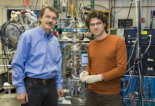
Alex Zettl (left) and Kenneth Jensen,

Caption: Alex Zettl (left) and Kenneth Jensen, using the same technology with which they created the world’s first fully functional nanotube radio, have created the world's smallest and most sensitive weighing scale.

Credit: photo by Roy Kaltschmidt, Berkeley Lab Public Affairs. Usage Restrictions: None.
One tip of the carbon nanotube is free and the other tip is anchored to an electrode in close proximity to a counter-electrode. A DC voltage source, such as from a battery or a solar cell array, is connected to the electrodes. Applying a DC bias creates a negative electrical charge on the free tip of the nanotube. An additional radio frequency wave "tickles" the nanotube, causing it to vibrate at a characteristic "flexural" resonance frequency.

When an atom or molecule is deposited onto the carbon nanotube, the tube's resonant frequency changes in proportion to the mass of the atom or molecule, much like the added mass of a diver changes the flexural resonance frequency of a diving board. Measuring this change in frequency reveals the mass of the impinging atom or molecule.

"Getting nanotubes to vibrate is fairly easy," said Jensen. "The difficult part is detecting those small vibrations. We accomplished this by field-emitting, or spraying, electrons from the tip of the nanotube and detecting the resulting electrical current."

Using their NEMS mass sensor, Zettl, Jensen and Kim were able to weigh individual gold atoms and measure masses as small as two fifths that of a gold atom at room temperature and in just a little more than one second of time. A gold atom has a mass of 3.25 x 10⁻²⁵ kilograms, which means that there are about 3 million million million million gold atoms in a single kilogram.

While there have been other NEMS that function as mass sensors before, most of these previous devices were fashioned from silicon, and none had achieved the magical single-atom resolution at room temperature. The carbon nanotube mass sensor of Zettl's group is a thousand times smaller by volume than typical NEMS resonators – measuring only about a billionth of a meter in diameter and 200 billionths of a meter in length.

"Carbon nanotubes are the ideal material for this purpose and their small size makes them sensitive enough to resolve single atoms even at room temperature," Jensen said.

While scientists already have the ability to measure the mass of individual atoms through a complex technique known as mass spectrometry, this new carbon nanotube NEMS mass sensor offers some distinct advantages and opens the door to new possibilities, as Jensen explained.

"Unlike mass spectrometry, our device does not require the ionization of neutral atoms or molecules that can destroy samples such as proteins. Also unlike mass spectrometers, our carbon nanotube mass sensor becomes more sensitive at higher mass ranges, which makes it more suitable for measuring large biomolecules like DNA. Finally, our device is small enough so that, in time, it could be incorporated onto a chip." ###

Zettl, Jensen and Kim described their NEMS mass sensor in a paper published in the journal Nature Nanotechnology, entitled: "An atomic-resolution nanomechanical mass sensor." This research was supported by the U.S. Department of Energy's Office of Science, Basic Energy Sciences Program's Materials Sciences and Engineering Division, and by the National Science Foundation within the Center of Integrated Nanomechanical Systems.

Contact: Lynn Yarris lcyarris@lbl.gov 510-486-5375 DOE/Lawrence Berkeley National Laboratory

Tags: or and

Saturday, August 30, 2008

Scientists demonstrate highly directional semiconductor lasers

QC Laswer with Plasmonic Collimator

Caption: A cartoon showing a quantum cascade laser patterned with a plasmonic collimator which greatly reduces the divergence in the vertical direction.

Credit: Courtesy of Capasso Lab, Harvard School of Engineering and Applied Sciences. Usage Restrictions: None.
Innovation opens the door to a wide range of applications in photonics and communications

CAMBRIDGE, Mass. – Applied scientists at Harvard University in collaboration with researchers from Hamamatsu Photonics in Hamamatsu City, Japan, have demonstrated, for the first time, highly directional semiconductor lasers with a much smaller beam divergence than conventional ones. The innovation opens the door to a wide range of applications in photonics and communications. Harvard University has also filed a broad patent on the invention.
Spearheaded by graduate student Nanfang Yu and Federico Capasso, Robert L. Wallace Professor of Applied Physics and Vinton Hayes Senior Research Fellow in Electrical Engineering, all of Harvard's School of Engineering and Applied Sciences (SEAS), and by a team at Hamamatsu Photonics headed by Dr. Hirofumi Kan, General Manager of the Laser Group, the findings were published online in the July 28th issue of Nature Photonics and will appear in the September print issue.
F. Capasso and Nanfang Yu

Caption: Harvard School of Engineering and Applied Sciences' reserachers Federico Capasso (red shirt) and Nanfang Yu working at the far-field measurement setup. Credit: Eliza Grinnell, Harvard School of Engineering and Applied Sciences. Usage Restrictions: None.
"Our innovation is applicable to edge-emitting as well as surface-emitting semiconductor lasers operating at any wavelength—all the way from visible to telecom ones and beyond," said Capasso. "It is an important first step towards beam engineering of lasers with unprecedented flexibility, tailored for specific applications. In the future, we envision being able to achieve total control of the spatial emission pattern of semiconductor lasers such as a fully collimated beam, small divergence beams in multiple directions, and beams that can be steered over a wide angle."
While semiconductor lasers are widely used in everyday products such as communication devices, optical recording technologies, and laser printers, they suffer from poor directionality. Divergent beams from semiconductor lasers are focused or collimated with lenses that typically require meticulous optical alignment—and in some cases bulky optics.

To get around such conventional limitations, the researchers sculpted a metallic structure, dubbed a plasmonic collimator, consisting of an aperture and a periodic pattern of sub-wavelength grooves, directly on the facet of a quantum cascade laser emitting at a wavelength of ten microns, in the invisible part of the spectrum known as the mid-infrared where the atmosphere is transparent. In so doing, the team was able to dramatically reduce the divergence angle of the beam emerging from the laser from a factor of twenty-five down to just a few degrees in the vertical direction. The laser maintained a high output optical power and could be used for long range chemical sensing in the atmosphere, including homeland security and environmental monitoring, without requiring bulky collimating optics.

"Such an advance could also lead to a wide range of applications at the shorter wavelengths used for optical communications. A very narrow angular spread of the laser beam can greatly reduce the complexity and cost of optical systems by eliminating the need for the lenses to couple light into optical fibers and waveguides," said Dr. Kan. ###

The team's other authors are graduate student Jonathan Fan, postdoctoral researchers Qijie Wang and Christian Pflügl, research associate Laurent Diehl—all from Harvard University—and researchers Tadataka Edamura and Masamichi Yamanishi—both from Hamamatsu Photonics.

The research was partially supported by Air Force Office of Scientific Research. The Harvard authors also acknowledge the support of Harvard's Center for Nanoscale Systems (CNS), a member of the National Nanotechnology Infrastructure Network (NNIN).

Supplementary Material

Lasers are often considered to be highly directional light sources: their beams are able to propagate over long distances without substantial spreading. This, however, is not always the case. Semiconductor lasers, the most commonly used among all lasers, suffer from a large beam divergence. Such divergence is governed by the principle of diffraction, which predicts bending and spreading of light around small obstacles or apertures. Light beams endure strong diffraction when emerging from the small light-emitting regions of semiconductor lasers (the dimensions of which are comparable to the laser wavelength). This leads to a beam divergence angle of tens of degrees for most semiconductor lasers.

Laser beams with small divergence angles are important for many applications such as free-space communication, remote sensing, and pointing. High directionality is desirable for efficiently coupling laser power into waveguides and optical fibers without the need for lenses. Beam collimation is usually achieved using lenses or other bulky optical devices that typically require meticulous alignment.

To create semiconductor lasers with highly directional output, the researchers incorporated a properly tailored metallic structure, named a plasmonic collimator, directly onto the laser facet. The plasmonic collimator consists of an aperture centered on the laser active region and a periodic array of grooves nearby, as shown in the figure. The aperture couples part of the emitted light into surface electromagnetic waves (so-called surface plasmons) on the laser facet. As the surface waves propagate on the facet, they are progressively scattered by the grooves and are reemitted into the far field.

These beams are in phase when they arrive at the same position in the far field, so that the optical energy is concentrated into a small solid angle. Stated slightly differently, grooves in the plasmonic collimator act essentially as an array of coherent light sources that interfere constructively so that optical energy is projected into the far field in a single direction perpendicular to the laser facet with small divergence. The collimation effect in the innovative laser resembles that of the phased antenna array (an array of antennas emitting in phase), which has already been widely used in applications such as directional broadcasting and space communication.

In the present work low beam divergence has been achieved in the vertical direction, parallel to the direction of the polarization of the laser. By replacing the metallic structure with a series of concentric grooves of circular shape one can achieve also a very small divergence in the horizontal direction. This will result in full beam collimation. Preliminary results have shown that this scheme works very well: a divergence of a few degrees in the horizontal and vertical planes has been achieved in a quantum cascade laser, in accordance with simulations.

Contact: Michael Patrick Rutter mrutter@seas.harvard.edu 617-496-3815 Harvard University

Tags: or and

Friday, August 29, 2008

University of Pennsylvania Researchers Demonstrate a Flexible, One-Step Assembly of Nanoscale Structures

methodologies for the controlled synthesis, fabrication
PHILADELPHIA –- Scientists at the University of Pennsylvania have created a one-step, repeatable method for the production of functional nanoscale patterns or motifs with adjustable features, size and shape using a single master “plate.”

Researchers took advantage of the elastic instability of a widely used, flexible polymer membrane, polydimethylsiloxane, or PDMS. When exposed to a solvent, circular pores in the membrane elliptically deform, and elastic interactions between them generate long-range orientational order of their axes into a “diamond plate” pattern. By lacing the solvent with iron nanoparticles, the team found that evaporation of the solvent drives the assembly of the nanoparticles onto the membrane surface along these distorted pores.

This results in two-dimensional patterns with sub-100 nanometer features. The traditional fabrication process can take as long as a month and cost $50,000 per print. In this new process, a master can be made for a fraction of the cost and can be reused many times. The Penn team’s technique does not require delicate surface preparation or the complex chemistry of standard lithographic processes. Instead, the new process relies on patterns that form spontaneously in equilibrium. The resulting, “diamond-plate” pattern persists over the entire sample, as large as a square centimeter, with no imperfections.

The features of the resultant nanoparticle patterns are up to 10 times sharper than the original membrane. The resulting symmetry of the film can be transferred onto a substrate, both flat or curved, where it can be used to generate similar anisotropic magnetic, photonic, phononic and plasmonic properties.

“These functional nano-motifs could in turn benefit novel technologies that are sensitive to local environment change such as smart clothing, biomarkers and eco-friendly buildings,” Shu Yang, assistant professor in the Department of Materials Science and Engineering of the School of Engineering and Applied Science at Penn, said. “Using similar pattern transformation principles, our technique could be extended to pattern a variety of material systems such as polymers and composites, creating a new design mechanism for nanoscale manufacturing.”

The team modeled the elastic instability of the membrane in terms of elastically interacting “dislocation dipoles” and found complete agreement between the theoretical ground state and the observed pattern. This model allows for the manipulation of the structural details of the membrane to tailor the elastic distortions and generate a variety of nanostructures.

The natural world provides many examples of the type of intrinsic, bottom-up effects that engineers see here, from the arrangement of growing leaves on a plant to the pattern of animal stripes to fingerprints. In these systems, instabilities, packing constraints and simple geometries drive the formation of delicate, detailed and beautiful patterns. Mechanical instabilities in soft polymers, precipitated by dewetting, swelling and buckling during the production stage, are often viewed as failure mechanisms that can interfere with the performance of devices. However, these instabilities are now being exploited to assemble complex patterns, to fabricate novel devices such as stretchable electronics and flexible microlenses and to provide a metrology for measuring elastic moduli and the thickness of ultrathin films.

PDMS membranes have been widely used in soft lithography for low-cost fabrication of microdevices. The Penn team replica-molded a PDMS membrane with circular pores from an array of 1 μm diameter silicon pillars spaced 2 μm apart on a square lattice. When exposed to the organic solvent toluene, PDMS gels swell by as much as 130 percent. As the osmotic pressure builds, the circular pores in the PDMS deform and eventually snap shut to relieve the stress, much as the joints in railways and bridges expand and contract to maintain structural integrity in response to changes in moisture and temperature.

Because the elastic deformation of the PDMS membrane is induced by solvent swelling, the diamond plate pattern in PDMS is stable in the wet state and snaps back to the original square lattice once the solvent evaporates. To capture the diamond plate before evaporation and, more important, to utilize this deformation for assembly of complex functional structures, the team suspended superparamagnetic Fe3O4 nanoparticles in toluene and applied the solution to the PDMS membrane. As the PDMS swells, the convective assembly of the nanoparticles follows, faithfully replicating the deformed PDMS membrane. Once dry, the elastic membrane returns to its original state and can be reused.

The study was published in the journal Nano Letters and was conducted by members of the Laboratory for Research on the Structure of Matter at Penn: Ying Zhang, Anna Peter, Pei-Chun Lin and Yang of the Department of Materials Science and Engineering and Elisabetta A. Matsumoto and Kamien of the Department of Physics and Astronomy.

Funding was provided by the National Science Foundation MRSEC Program and an NSF Career Award bestowed upon Yang. ###

Contact: Jordan Reese jreese@upenn.edu 215-573-6604 University of Pennsylvania

Tags: or and

Thursday, August 28, 2008

NIST trumps the clumps: Making biologic drugs safer

protein based drugs

NIST researchers have developed methods and adapted techniques that will allow the pharmaceutical industry to monitor the formation of potentially dangerous aggregates in protein-based drugs. Image Copyright: IoanaDrutu
Scientists at the National Institute of Standards and Technology (NIST) have developed a technique to measure the formation of clumps of proteins in protein-based pharmaceuticals. This first systematic study* clarifies the conditions under which scientists can be assured that their instruments are faithfully measuring the formation of protein aggregates, a major concern because of its impact on quality control and safety in biologic drug manufacturing.
Proteins, a main constituent of many new drugs, are large molecules that have a tendency to stick to each other and form clumps during their manufacture. These clumps have been associated with severe immune responses. In at least one case, the inadvertent creation of protein clumps during the processing of a drug to treat anemia caused an immune reaction in about 250 patients that destroyed their ability to produce red blood cells. Those patients now have to receive blood transfusions every few days to replenish these vital cells.

Events such as this led the Food and Drug Administration to call for the development of sensitive and rapid measurement tools that can detect aggregation of protein drugs during the manufacturing phase. To address the problem, NIST researchers hit upon the idea of adapting a technique known as electrospray differential mobility analysis (ES-DMA). Commonly used to size soot and other aerosols, ES-DMA uses an electric current to vaporize a solution of proteins into tiny charged water droplets, each containing a single protein molecule or protein aggregate. Once these droplets evaporate, the charged proteins and protein aggregates are drawn into an oppositely charged tube. By making controlled adjustments to the voltage of the tube and the velocity of the air flowing through it, researchers can collect particles of a specific size, allowing the proteins and protein aggregates to be precisely sorted and counted.

The NIST team adapted the technique for biopharmaceutical applications. According to researcher Leonard Pease, ES-DMA is tricky to get right, but the NIST team was able to define the conditions needed to electrospray proteins and protein aggregates reliably and repeatedly. NIST scientists favor ES-DMA for its ability to quickly resolve particle sizes differing by as little as 0.2 nanometers, to provide a direct measure of particle size distributions, and to accept bioreactor samples with significantly reduced preparation requirements.

In addition to sizing proteins, Pease said the technique could also be used to accurately size many different types of particles used in medicine, such as the viruses used in the human papillomavirus (HPV) vaccine and gene therapy. “The adaptation of this technology is just one of many excellent examples of how NIST seeks out and works with U.S. industry,” says Willie E. May, director of the NIST Chemical Science and Technology Laboratory. ###

* L. Pease, J. Elliott, D. Tsai, M. Zachariah and M. Tarlov. Determination of protein aggregation with differential mobility analysis: application to IgG antibody. Biotechnology and Bioengineering. Available online at dx.doi.org/10.1002/.

Contact: Mark Esser mark.esser@nist.gov 301-975-8735 National Institute of Standards and Technology (NIST)

Tags: or and

Wednesday, August 27, 2008

Cool! Nanoparticle research points to energy savings

Nanoparticle Research Points to Energy Savings

Caption: Nanoparticle additives to lubricants commonly combined with refrigerants used in chillers may encourage secondary nucleation -- bubbles on top of bubbles. The double-bubble effect enhances boiling heat transfer and, ultimately, could help to boost the energy efficiency of industrial-sized cooling systems.

Credit: NIST. Usage Restrictions: None.
Adding just the right dash of nanoparticles to standard mixes of lubricants and refrigerants could yield the equivalent of an energy-saving chill pill for factories, hospitals, ships, and others with large cooling systems, suggest the latest results from National Institute of Standards and Technology (NIST) research that is pursuing promising formulations.

NIST experiments with varying concentrations of nanoparticle additives indicate a major opportunity to improve the energy efficiency of large industrial, commercial, and institutional cooling systems known as chillers.
These systems account for about 13 percent of the power consumed by the nation’s buildings, and about 9 percent of the overall demand for electric power, according to the Department of Energy.

NIST researcher Mark Kedzierski has found that dispersing “sufficient” amounts of copper oxide particles (30 nanometers in diameter) in a common polyester lubricant and combining it with an equally pedestrian refrigerant (R134a) improves heat transfer by between 50 percent and 275 percent. “We were astounded,” he says.

Results of this work have been presented at recent conferences and will be reported in an upcoming issue of the ASME Journal of Heat Transfer.

Just how nanomaterial additives to lubricants improve the dynamics of heat transfer in refrigerant/lubricant mixtures is not thoroughly understood. The NIST research effort aims to fill gaps in knowledge that impede efforts to determine and, ultimately, predict optimal combinations of the three types of substances.

“As with all good things, the process is far from foolproof,” Kedzierski explains. “In fact, an insufficient amount or the wrong type of particles might lead to degradation in performance.”

On the basis of work so far, the researcher speculates several factors likely account for nanoparticle-enabled improvements in heat-transfer performance. For one, nanoparticles of materials with high thermal conductivity improve heat transfer rates for the system. Preliminary results of the NIST research also indicate that, in sufficient concentrations, nanomaterials enhance heat transfer by encouraging more vigorous boiling of the mixture. The tiny particles stimulate, in effect, double bubbles—secondary bubbles that form atop bubbles initiated at the boiling site. Bubbles carry heat away from the surface, and the fact that they’re being formed more efficiently because of the nanoparticles means the heat gets transferred more readily.

Other interactions, Kedzierski says, also are likely to contribute to the dramatic performance improvements reported at NIST and elsewhere.

Success in optimizing recipes of refrigerants, lubricants and nanoparticle additives would pay immediate and long-term dividends. If they did not harm other aspects of equipment performance, high-performance mixtures could be swapped into existing chillers, resulting in immediate energy savings. And, because of improved energy efficiency, next-generation equipment would be smaller, requiring fewer raw materials in their manufacture. ###

Contact: Mark Bello mark.bello@nist.gov 301-975-3776 National Institute of Standards and Technology (NIST)

Tags: or and

Tuesday, August 26, 2008

'Nanonet' circuits closer to making flexible electronics reality

flexible circuits created using carbon nanotubes

Caption: These are two photos of flexible circuits created using carbon nanotubes in research at Purdue University and the University of Illinois at Urbana-Champaign. The researchers have overcome a major obstacle in producing transistors from networks of carbon nanotubes, a technology that could make it possible to print circuits on plastic sheets for applications including flexible displays and an electronic skin to cover an entire aircraft to monitor crack formation.

Credit: University of Illinois at Urbana-Champaign. Usage Restrictions: None. High Resolution Image
WEST LAFAYETTE, Ind. - Researchers have overcome a major obstacle in producing transistors from networks of carbon nanotubes, a technology that could make it possible to print circuits on plastic sheets for applications including flexible displays and an electronic skin to cover an entire aircraft to monitor crack formation.

The so-called "nanonet" technology - circuits made of numerous carbon nanotubes randomly overlapping in a fishnet-like structure - has been plagued by a critical flaw: The network is contaminated with metallic nanotubes that cause short circuits.
The discovery solves this problem by cutting the nanonet into strips, preventing short circuits by breaking the path of metallic nanotubes.

"This is a fundamental advance in how nanotube circuits are made," said Ashraf Alam, a professor of electrical and computer engineering at Purdue University. He is working with Kaushik Roy, Purdue's Roscoe H. George Professor of Electrical and Computer Engineering, and doctoral students Ninad Pimparkar and Jaydeep P. Kulkarni.

Researchers at the University of Illinois at Urbana-Champaign led experimental laboratory research to build the circuits, and Purdue led research to develop and use simulations and mathematical models needed to design the circuits and to interpret and analyze data.

Findings will be detailed in a research paper appearing in the journal Nature on July 24. The paper was written by the Purdue engineers and University of Illinois researchers : John A. Rogers, Founder Professor of Materials Science and Engineering and a professor of chemistry; Moonsub Shim, Racheff Assistant Professor of Materials Science and Engineering; and doctoral students Qing Cao, Hoon-sik Kim and Congjun Wang.

"These findings represent the culmination of four years of collaborative efforts between the Illinois and Purdue groups," Rogers said. "The work established the fundamental scientific knowledge that led to this particular breakthrough and the ability to make circuits."

The nanonets are made of tiny semiconducting cylinders called single walled carbon nanotubes. Metallic nanotubes form unavoidably during the process of making carbon nanotubes. These metal tubes then link together in meandering threads that eventually stretch across the width of the transistor, causing a short circuit.

"Other researchers have proposed eliminating the metallic nanotubes," Rogers said. "Instead, we found a very nice way of essentially removing the effect of these metallic nanotubes without actually eliminating them."

The researchers created a flexible circuit containing more than 100 transistors, the largest nanonet ever produced and the first demonstration of a working nanonet circuit, Alam said.

"Now there is no fundamental reason why we couldn't develop nanonet technologies," he said. "If you can make a flexible circuit with 100 transistors, you can make circuits with 10,000 or more transistors."

The advance may allow researchers to use carbon nanotube transistors to create high-performance, shock-resistant, lightweight and flexible integrated circuits at low cost, Alam said.

A key advantage of the nanonet technology is that it can be produced at low temperatures, enabling the transistors to be placed on flexible plastic sheets that would melt under the high temperatures required to manufacture silicon-based transistors, he said.

Possible applications include an electronic skin that covers an aircraft and automatically monitors the formation of cracks to alert technicians and prevent catastrophic failures.

Such shape-conforming electronics are not possible using conventional silicon-based circuits, which are manufactured on rigid wafers or glass plates.

"Now electronics are flat, which limits their utility since most objects in real life are not flat," Roy said.

Flexible displays could be integrated into automotive windshields to provide information for drivers. Other potential applications include "electronic paper" that displays text and images, solar cells that could be printed on plastic sheets and television screens capable of being rolled up for transport and storage.

"For these types of applications, manufacturers might literally print, or stamp, circuits onto plastic sheets, like the roll-to-roll printing used to print newspapers," Alam said.

Conventional circuits for flat-panel televisions contain transistors made of materials called polysilicon or amorphous silicon, which cannot be used in flexible applications.

Nanonet transistors are promising for so-called macroelectronics because they are best suited for large-scale applications, but these transistors may not be as well suited for the requirements of microelectronic circuits, such as those in computer chips, Alam said.

The nanotubes are arranged randomly and overlap each other like tiny needles. If the nanonet area is large enough, the overlapping metallic nanotubes will eventually form a meandering string across the entire transistor, causing a short circuit. But if the device is segmented into strips, this meandering path of metallic rods is cut at the point where the lines separate one strip from another, preventing short circuits.

The metallic nanotubes make up about one-third of the nanotubes in the transistor. Because the carbon nanotubes are twice as numerous as the metallic tubes, enough of them exist to form a complete circuit. The models and simulations are needed to tell researchers precisely how wide to make the strips so that the pathway of metallic tubes is cut but the carbon nanotubes complete their circuit.

"The theory and simulation work done at Purdue shows there is always a way to break the metallic path and still keep the semi conducting carbon-nanotube path intact," Alam said. "The teams at Illinois and Purdue continuously provide insights about why things work the way they do and how to make them work better through combined modeling and experimental efforts."

Each nanonet transistor consists of numerous strips of nanotubes, separated bylines that are etched in place. The lines are easy to create with a standard etching process used in the semiconductor industry.

Future research may include work focusing on learning the reliability of the carbon nanotube circuits.

The research has been funded by the National Science Foundation through the Network for Computational Nanotechnology at the Birck Nanotechnology Center in Purdue's Discovery Park. The Illinois portion of the research also was funded and supported by the NSF, U.S. Department of Energy, Motorola Corp., and by the university's Frederick Seitz Materials Research Lab, the Center for Microanalysis of Materials and the Department of Chemistry.

The researchers used computers made available by a global network called the nanoHUB, an Internet-based science gateway that provides computer-based resources for research and education in the areas of nanoelectronics and nanoelectromechanical systems and their application to nano-biosystems.

"This work requires tremendous computing resources because these are not trivial calculations," Alam said.

Nanoelectronics focuses on creating a class of electronic devices containing features measured in nanometers, equivalent to one-billionth of a meter. A nanometer is about the size of 10 atoms strung together.

The Network for Computational Nanotechnology uses advanced theory and simulations to explore new ideas for digital switching devices such as innovative types of transistors that promise to help researchers create future electronics. ###

The research is complementary to work by Purdue researcher David Janes, a professor of electrical and computer engineering. His work involves transparent circuits using a different type device called nanowires, made of indium oxide instead of carbon nanotubes.

Related Web sites: Contact: Emil Venere venere@purdue.edu 765-494-4709 Purdue University

Monday, August 25, 2008

Cancer drug delivery research at Case Western Reserve University speeds time from two days to two hours

Yu Cheng and Clemens BurdaPaper discusses gold nanoparticle system that takes drug right to cancerous cells

Researchers at Case Western Reserve University have developed a technique that has the potential to deliver cancer-fighting drugs to diseased areas within hours,
as opposed to the two days it currently takes for existing delivery systems.

Using laboratory mice, drug delivery time from injection to the cancer cells was reduced from two days to mere hours. Using this as a model for potential human use, cancer patients may someday soon receive the benefits of cancer-fighting drugs within hours of injection.

Findings are discussed in a paper, co-authored by Clemens Burda, associate professor of chemistry and director of the Center for Chemical Dynamics and Nanomaterials Research at Case Western Reserve University and graduate student Yu Cheng, appearing in the current edition of the Journal of the American Chemical Society .

The system uses gold nanoparticle vectors to deliver photodynamic therapy (PDT) drugs through the bloodstream to cancerous sites.

"Gold nanoparticles are usually not used for the PDT drug vector," said Cheng. "However, gold is chemically inert and nontoxic."

Photodynamic therapy utilizes light-sensitive drugs that, when exposed to light of a certain wavelength, will energize and burn away cancer cells.

Because exposure to light activates these drugs, PDT patients must keep out of bright lights for days while the drugs make their way through the bloodstream to the cancer site. At that time, they are activated by a light focused on the specific area of the body.

"By shortening the waiting time from drug injection to activation, PDT patients are much less inconvenienced and tend to have a more normal lifestyle," said Burda.
Looks like a "Hairy Ball"

The drug delivery system uses a gold nanoparticle (Au NP) as its hub. Gold is non-toxic to the human body, and has a versatile surface chemistry, large surface-to-volume ratio and variable size and shape.

Each Au NP is coated with polyethylene glycol (PEG) ligands, giving it the appearance of a hairy ball, said Burda. These PEG molecules offer several advantages over other materials: they are soluble in fats and water, don't interact with proteins in the bloodstream and help protect the drug, keeping it safe and stable until delivery to the cancer site.

Between each PEG ligand, molecules of a photodynamic chemotherapy drug (Pc 4) are attached to the Au NP. The Pc 4 drug (a phthalocyanine compound) was developed at Case Western Reserve by Malcolm Kenney, professor of chemistry.

When the nanoparticle reaches the cancerous tissue the drug molecules are released and uploaded to the diseased area. Focused red light is used to energize the drug in the patient once it has been delivered to the tumor.

Burda says that a potential future research project would look at providing a time-release administration of the drug rather than a more all-at-once release. In the long term, Burda hopes to make the Au NP delivery system applicable to a broad range of diseases.

The Au NP has a diameter of 5 nm. The addition of PEG ligands expands the total diameter to 32 nm, larger than some other nanoparticles currently in use, but still small enough to pass unencumbered through the bloodstream.

A single 1/4-mL injection holds approximately 100 million Au NPs, each carrying approximately 100 drug molecules.
Tail to Tumor in Two Minutes

In the laboratory of Baowei Fei, assistant professor of radiology and biomedical engineering at Case Western Reserve, these Au NPs have been used to treat mice with cancerous tumors. Once the Au NPs have been injected into the tail, the Pc 4 is uploading into the diseased area within minutes. The accelerated speed of drug administration in mice is due in part to the much more efficient dispersion of the NP delivered drug.

When tested on human cells called HeLa — a line of laboratory-grown human cells used in testing — most of the drug is uploaded within one hour.

Testing on human beings may not begin for some time. Commercialization will take even longer due to Food and Drug Administration (FDA) testing and approval. However, all of the components — Au Nps, PEG ligands and Pc 4 — have already received FDA approval.
What's Next

Burda says that as Au NP testing continues, short-term goals include minimizing the amount of material and drug load needed for effective interaction with cancer cells; optimizing potential targeting systems on the PEG ligands for faster, even more specific placement in diseased areas; and increasing the overall effectiveness of nanoparticle enhanced therapy.

"The system is very modular," says Burda. "We can change the size and shape of the Au core NPs and we can change the functionality of the PEG ligands. This should lead to optimization of the drug targeting and therapy. If our research is successful, other researchers might adapt this drug delivery system to other diseases and applications."

Funding support came from the National Science Foundation, National Institute of Health/National Cancer Institute and the Biomedical Research Technology Transfer Center under the leadership of Pamela Davis, dean of the Case Western Reserve School of Medicine and vice president for medical affairs.

Contact: Susan Griffith susan.griffith@case.edu 216-368-1004 Case Western Reserve University

Sunday, August 24, 2008

A phonon floodgate in monolayer carbon

STM Graphene Spectra

Caption: These STM electron tunneling spectra were obtained at the same physical location on a graphene surface held at different gate voltages. The vertical scale gives a measure of the energy-dependent graphene electron density of states; the different curves result from the different applied gate voltages. Changing the gate voltage allows the density of charge carriers in the graphene to be controllably varied. The red arrows indicate the measured tunnel current signal that occurs when electrons tunnel from the STM tip to the graphene Dirac point, a minimum in the graphene density of states.

Credit: Lawrence Berkeley National Laboratory. Usage Restrictions: None
The first STM spectroscopy of graphene flakes yields new surprises

BERKELEY, CA — Scientists at the U.S. Department of Energy's Lawrence Berkeley National Laboratory (Berkeley Lab) and the University of California at Berkeley have performed the first scanning tunneling spectroscopy of graphene flakes equipped with a "gate" electrode. The result is the latest in a series of surprising insights into the electronic behavior of this unique, two-dimensional crystal form of carbon: an unexpected gap-like feature in the energy spectrum of electrons tunneling into graphene's single layer of atoms.

Michael Crommie, a faculty scientist in Berkeley Lab's Materials Sciences Division and a professor in the Department of Physics at UC Berkeley, explains that this peculiar feature of the electronic structure of graphene arises from the interaction of the tunneling electrons with phonons, the quantized vibrations of the 2-D graphene crystal, and may lead to novel applications for future graphene nanodevices.
A team led by Yuanbo Zhang, a postdoctoral fellow in Crommie's research group, discovered graphene's mysterious energy gap; the research appears in advanced online publication on the Nature Physics website at dx.doi.org/10.1038/nphys1022.
"Monolayer graphene – flakes a single atom thick — were first isolated by Andrew Geim's group at the University of Manchester, England, in 2005, and have been intensely studied since then," says Crommie. "Graphene's interesting electronic effects opens a new realm of basic science. It's an entirely new material, with new physics that could lead to new practical devices and applications. In that respect it's as promising as carbon nanotubes — but graphene's planar geometry is potentially even more versatile."

Caption: Melissa Panlasigui, Michael Crommie, Yuanbo Zhang, and Victor Brar are among the members of Crommie's group and colleagues who discovered graphene's phonon floodgate. Not pictured are authors Feng Wang, Caglar Girit, Yossi Yayon, and Alex Zettl.

Credit: Roy Kaltschmidt, Lawrence Berkeley National Laboratory. Usage Restrictions: None.
Crommie says, "Because graphene is two-dimensional, it can be carved up and cut into tailored shapes, like cutting a sheet of paper." The shape might include features like narrow sections to control the flow of electrons, edges with unique magnetic properties, and dopant atoms implanted at precise locations in the 2-D matrix.
graphene 50 microns (millionths of a meter) long rests on a substrate of silicon

Caption: Under the STM tip a flake of graphene 50 microns (millionths of a meter) long rests on a substrate of silicon with a thin layer of silicon dioxide insulation (upper left). The graphene is contacted by gold electrodes, connected to outside experimental equipment and to the underlying silicon electrode, which is used to apply a gate voltage. At lower right, a topographical image of the graphene flake, 10 nanometers (billionths of a meter) across. Variations in height of one or two angstroms (ten-billionths of a meter) are likely caused by the roughness of the substrate.

Credit: Lawrence Berkeley National Laboratory. Usage Restrictions: None.
"Two-dimensionality confers an amazing degree of flexibility," he says, "but to take full advantage of this new material, we will need to understand what is happening at atomic length scales. That's where the STM — the scanning tunneling microscope — comes in."

Studying gated graphene with the STM

The business end of the STM is the tip, a fine metal wire placed in close proximity to a conducting surface — in this case a flake of graphene contacted by thin metal electrodes. An applied voltage between the tip and sample causes electrons to tunnel between them — a "tunnel current." At constant voltage the tunnel current depends on the position of the tip with respect to the surface, so by scanning the tip across the flake the surface topography can be mapped.
The current can also be varied by changing the voltage between tip and surface, which gives information about the electronic structure of the material — in particular the local density of states (LDOS, an energy-dependent electron density) below the tip. Combining STM microscopy and spectroscopy allows a researcher to construct an image of the spatial distribution of the electronic states.

The Crommie group's experiments used exfoliated graphene, individual flakes made by mechanically cleaving a sheet of atoms from a larger chunk of carbon. The group attached electrodes to both the graphene flake and an underlying substrate consisting of a conducting layer of silicon, which was separated from the flake by an insulating layer of silicon dioxide. The experimental setup was thus able to uniquely incorporate two distinct voltage differences, that between the tip of the STM and the surface (the "bias" voltage) and that between the graphene flake and the underlying substrate (the "gate" voltage).

"The purpose of controlling the gate voltage is to vary the density of the charge carriers in the graphene," Crommie says. "The purpose of varying the STM bias voltage is to perform spectroscopy, so we can look at the graphene's local density of states at different energies. We want to know where are the electrons? How are they behaving?"

These questions are of particular interest because of graphene's odd electronic properties. The carbon atoms in graphene are arranged at the corners of hexagons, as in chicken wire, with three of each atom's four electrons involved in molecular bonds with its neighbors; these are sigma orbitals that lie in the plane of the material. The remaining electrons are in pi orbitals extending above and below the plane. The hybridization of the pi orbitals spreads across the graphene sheet, and the unconfined electrons are free to move as high-speed "relativistic quasiparticles," so-called Dirac fermions which act as if they have no mass.

The plot of energy states for Dirac fermions in graphene looks quite different from that of a conventional 3-D semiconductor, which typically consists of two opposing parabolic curves, a lower-energy valence band and a higher-energy conduction band, with a band gap between them that no charge carriers can occupy.

Graphene's unusual electronic properties

By contrast, the Dirac fermion energy states of graphene can be represented as two cones with their vertices meeting at a point of minimum electronic density, called the Dirac point. Thus one might expect the spectrum of the density of states resulting from electrons tunneling into graphene to be linear, following the smooth edge of the touching cones.

"When we plotted the LDOS spectra of our gated graphene flakes, however, we found a gap-like feature that was centered on the Fermi energy — no matter how we changed the density of charge carriers in the graphene with the gate voltage and no matter where we looked on the flake," Crommie says.

The Fermi energy is the energy of the highest occupied electronic state in a graphene flake, and is the reference energy for this kind of measurement. "Almost no electrons tunneling from the STM tip could enter the graphene at low energies within this gap region, but at slightly higher energies there was an abrupt, giant enhancement in tunneling, like a floodgate opening up for electrons." And this was not the only odd feature in the graphene spectrum.

"There was another feature in the spectrum, a local minimum of states, which moved in a very regular way as we changed the gate voltage and thus the density of charge carriers in the material," Crommie says. The research team was able to unambiguously identify this feature as the mark of electrons tunneling from the STM tip to the Dirac point itself, the minimum in graphene density of states.

And what of the mystery gap itself? "We realized that this is not a true energy gap; it is not a feature of the electronic band structure of graphene," Crommie says. "Rather it marks the interaction of the tunneling electrons with phonons, the quantized vibrations of the graphene lattice."

Naturally occurring vibrations in the graphene sample are minimal for the Crommie group's STM setup, since it is kept very cold (just four degrees above absolute zero). However, when the bias voltage between the tip and graphene sample increased above a special threshold of 63 millivolts, "then each tunneling electron is able to create a phonon vibration in the graphene sheet, which allows the electron to get into the graphene much easier," Crommie says.

Indeed, this "phonon-assistance" causes the electron tunneling conductance to suddenly increase by more than 10 times, as phonons essentially open a new channel for electrons to flow through. Says Crommie, "We call it a phonon floodgate."

An underlying cause for this new channel arises from the carbon sigma orbitals, which normally don't conduct electrons (as the pi orbitals do), but which are brought into play when the graphene sheet vibrates. "When a phonon is created, the sigma orbital kind of rubs up against the pi orbital and acts like grease to help insert a tunneling electron into graphene," Crommie says.

"We started this research by simply asking, what do you see when you measure a graphene device with STM?" Crommie says. "In the process, we discovered a completely unexpected phonon floodgate. This gives us new insight into how electrons and phonons behave in graphene and creates new opportunities for future graphene-based nanodevice applications." ###

"Giant phonon-induced conductance in scanning tunneling spectroscopy of gate-tunable graphene," by Yuanbo Zhang, Victor W. Brar, Feng Wang, Caglar Girit, Yossi Yayon, Melissa Panlasigui, Alex Zettl, and Michael F. Crommie, appears in the advance online publication of Nature Physics at dx.doi.org/10.1038/nphys1022.

This research was sponsored by the U.S. Department of Energy's Office of Science.

Berkeley Lab is a U.S. Department of Energy national laboratory located in Berkeley, California. It conducts unclassified scientific research and is managed by the University of California. Visit our website at www.lbl.gov.

Contact: Paul Preuss paul_preuss@lbl.gov 510-486-6249 DOE/Lawrence Berkeley National Laboratory

Tags: or and

Saturday, August 23, 2008

Molecular hula hoop

Molecular Rotor

Caption: The rotary movement of a chromophore-modified alpha-cyclodextrin (alpha-CD) was studied in a rotaxane structure attached to a glass substrate. The rotary movement of the alpha-CD was demonstrated by defocused wide-field imaging with total internal reflection fluorescence microscopy. The motion of the alpha-CD is suspended in the dry state, whereas a fast rotary movement/rotary vibration is observed in the wet state.

Credit: (C) Wiley-VCH 2008. Usage Restrictions: Permission to use with appropriate credit and link to dx.doi.org
Spinning motion of a molecular rotor detected, Humans have long been trying to make the dream of nanoscopic robots come true. The dream is, in fact, taking on some aspects of reality. Nanoscience has produced components for molecular-scale machines. One such device is a rotor, a movable component that rotates around an axis.

Trying to observe such rotational motion on the molecular scale is an extremely difficult undertaking. Japanese researchers at the Universities of Osaka and Kyoto have now met this challenge.
As Akira Harada and his team report in the journal Angewandte Chemie, they were able to get "snapshots" of individual molecular rotors caught in motion.

As the subject of their study the researchers chose a rotaxane. This is a two-part molecular system: A rod-shaped molecule is threaded by a second, ring-shaped molecule like a cuff while a stopper at the end of the rod prevents the ring from coming off. The researchers attached one end of the rod to a glass support. To observe the rotational motions of the cuff around the sleeve, the scientists attached a fluorescing side chain to the cuff as a probe.

To observe the rotation of the ring around the rod, the researchers used a microscopic technique called defocused wide-field total internal reflection fluorescence microscopy. This gave snapshots of individual rotaxane molecules in the form of emission patterns. In simplified terms, if the cuff is motionless, the patterns make it possible to calculate the direction in which the probe emits its fluorescent light. This makes it possible to calculate the orientation of the cuff, which remains constant for every snapshot. However, if the cuff is rotating, the emission pattern does not reveal the spatial orientation of the probe.

The researchers showed that the cuff of the rotaxane does not rotate if the sample is dry. However, when it is wet they can see very rapid rotational and vibrational motion. The cuff rotates faster than the time required to snap a picture: the rotational speed is thus over 360° in 300 milliseconds. ###

Author: Akira Harada, Osaka University (Japan), chem.sci.osaka-u.ac.jp/lab/ Title: Single-Molecule Imaging of Rotaxanes Immobilized on Glass Substrates: Observation of Rotary Movement Angewandte Chemie International Edition 2008, 47, No. 32, 6077?, doi: 10.1002/anie.200801431

Contact: Akira Harada harada@chem.sci.osaka-u.ac.jp 81-668-505-445 Wiley-Blackwell

Tags: or and

Friday, August 22, 2008

'Nanosculpture' could enable new types of heat pumps and energy converters

branched nanorods

Caption: Researchers have discovered a new method to create branched nanorods, such as those in this scanning electron microscope image. Such nanorods could one day enable new nanoscale thermoelectric devices for power generation, as well as nanoscale heat pumps for cooling hot spots in nanoelectronics devices. Credit: Rensselaer/Ramanath. Usage Restrictions: Please include photo credit.
Researchers discover method to induce, suppress 'branching' of nanorods

Troy, N.Y. – A new technique for growing single-crystal nanorods and controlling their shape using biomolecules could enable the development of smaller, more powerful heat pumps and devices that harvest electricity from heat.

Researchers at Rensselaer Polytechnic Institute have discovered how to direct the growth of nanorods made up of two single crystals using a biomolecular surfactant. The researchers were also able to create "branched" structures by carefully controlling the temperature, time, and amount of surfactant used during synthesis.
"Our work is the first to demonstrate the synthesis of composite nanorods with branching, wherein each nanorod consists of two materials — a single-crystal bismuth telluride nanorod core encased in a hollow cylindrical shell of single-crystal bismuth sulfide," said G. Ramanath, professor of materials science and engineering at Rensselaer and director of the university's Center for Future Energy Systems, who led the research project. "Branching and core-shell architectures have been independently demonstrated, but this is the first time that both features have been simultaneously realized through the use of a biomolecular surfactant."

Most nanostructures comprised of a core and a shell generally require more than one step to synthesize, but these new research results demonstrate how to synthesize such nanorods in only one step.

"Our single-step synthesis is an important development toward realizing large-scale synthesis of composite nanomaterials in general," said Arup Purkayastha, who worked on the project as a postdoctoral researcher at Rensselaer and is now a scientist with Laird Technologies in Bangalore, India.

Because of their attractive properties, core-shell nanorods are expected to one day enable the development of new nanoscale thermoelectric devices for power generation, as well as nanoscale heat pumps for cooling hot spots in nanoelectronics devices.

"Our discovery enables the realization of two very important attributes for heat dissipation and power generation from heat," Ramanath said. "First, the core-shell junctions in the nanorods are conducive for heat removal upon application of an electrical voltage, or generating electrical power from heat. Second, the branched structures open up the possibility of fabricating miniaturized conduits for heat removal alongside nanowire interconnects in future device architectures."

The researchers discovered that synthesis at high temperatures or with low amounts of the biomolecular surfactant L-glutathonic acid (LGTA) yields branched nanorod structures in highly regulated patterns. In contrast, synthesis at low temperatures or with high levels of LGTA results in straight nanorods without any branching. It is interesting to note that at the point of branching, atoms in the branch resemble a mirror image of the parent crystal – a finding that reinforces Ramanath's conclusion that LGTA is able to induce branching through atomic-level sculpture.

"Since LGTA is similar to biological molecules, our discovery could be conceivably used as a starting point to explore the use of proteins and enzymes to atomically sculpt such nanorod architectures through biological processes," said Ramanath ###

Results of the study, titled "Surfactant-Directed Synthesis of Branched Bismuth Telluride/Sulfide Core/Shell Nanorods," were recently published online and will be featured in an upcoming issue of the journal Advanced Materials.

The full study may be viewed at: dx.doi.org/10.1002

Along with Ramanath and Purkayastha, co-authors of the paper include: Theodorian Borca-Tasciuc, associate professor of mechanical, aerospace and nuclear engineering at Rensselaer; Rensselaer materials science and engineering postdoctoral researcher Huafang Li; Rensselaer graduate students Makala S. Raghuveer and Darshan D. Gandhi; as well as materials science and engineering professor Raju V. Ramanujan, assistant professor Qingyu Yan, and postdoctoral researcher Zhong W. Liu of Nanyang Technological University in Singapore.

The research project was supported by the Interconnect Focus Center New York through MARCO, DARPA and New York state. The National Science Foundation and Honda Motor Co. also supported this project through research grants.

About Rensselaer

Rensselaer Polytechnic Institute, founded in 1824, is the nation's oldest technological university. The university offers bachelor's, master's, and doctoral degrees in engineering, the sciences, information technology, architecture, management, and the humanities and social sciences. Institute programs serve undergraduates, graduate students, and working professionals around the world.

Rensselaer faculty are known for pre-eminence in research conducted in a wide range of fields, with particular emphasis in biotechnology, nanotechnology, information technology, and the media arts and technology. The Institute is well known for its success in the transfer of technology from the laboratory to the marketplace so that new discoveries and inventions benefit human life, protect the environment, and strengthen economic development.

Contact: Michael Mullaney mullam@rpi.edu 518-276-6161 Rensselaer Polytechnic Institute

Tags: or and

Thursday, August 21, 2008

UC San Diego Launches Institute of Engineering in Medicine to Accelerate Health Care Tech

Shu Chien, professor of bioengineering and medicine

Shu Chien, professor of bioengineering and medicine, is the founding director of the Institute of Engineering in Medicine. To watch a Flash video introduction to IEM, click here for the IEM home page .
San Diego, CA, -- The world's top engineers, physicians and scientists are joining forces to conceptualize, develop and bring to reality the future tools and treatments of 21st century health care through UC San Diego's new Institute of Engineering in Medicine. Nanoparticle bombs to kill cancer, molecular-sized bridges to repair damaged hearts, and scarless surgery techniques are now on the frontier of medical innovations in California with the new Institute leading the way.
"As is our tradition at UC San Diego, we are bringing together diverse fields of science to catalyze innovation in unconventional ways," said Marye Anne Fox, chancellor of UC San Diego. "The goal of this new organized research unit is to improve health care delivery through new tools, technologies and medicines."

"This is an important step toward the integration of two academic and professional disciplines that increasingly share common goals," said Shu Chien, M.D., Ph.D., professor of bioengineering and medicine, and founding director of the Institute at UC San Diego. "The Institute has already attracted a large number of outstanding faculty from UC San Diego's Schools of Medicine, Pharmacy, and Jacobs School of Engineering, who all share the objective of translating creative ideas into clinical medicine and products that will transform patient care."

The Institute of Engineering in Medicine will intersect broad areas of research and focus on new approaches to disease identification, genomic medicine, clinical testing and monitoring, and the discovery of new drugs and therapies. The Institute aligns programs that are rated among the nation's best in U.S. News and World Report's annual "Top Graduate Schools" ranking, with the Jacobs School of Engineering ranked 11th, its bioengineering program ranked 2nd, and the School of Medicine ranked 14th among comparable graduate programs throughout the nation. UC San Diego is one of four universities in the nation with a medical school and engineering school both ranked in the top 15.

David Brenner, M.D., vice chancellor for Health Sciences and dean of the School of Medicine at UC San Diego, sees the Institute of Engineering in Medicine as a leader in designing next-generation therapies and devices.

"The next giant leap in patient care is going to happen through the joint efforts of engineering, medicine and pharmacy specialists, applying their expertise to expand the tool box for preventing, diagnosing and treating disease and injury," said Brenner. "Even though this formalized effort is still in its formative stage, we're already seeing exciting results from these collaborations that will have a profound impact at the patient's bedside."

"With our top-ranked engineering and medical schools and our close ties to the region's strong life sciences and technology industries, UC San Diego is uniquely positioned to make significant contributions to the advancement of technologies to improve medicine and save lives," said Frieder Seible, dean of the UC San Diego Jacobs School of Engineering and co-chair of the Calit2 Governing Board. "The ideas and applications generated by the Institute will be aided by an entrepreneurism center that has been recognized as a national model of effectiveness, and we will strive to move medical innovations out of the university and into patient care as quickly as possible."

The von Liebig Center for Entrepreneurism and Technology Advancement and the Office of Technology Transfer and Intellectual Property Services at UC San Diego, which have helped to spin off dozens of local biotech companies, will facilitate the process of commercializing the Institute's innovations.

Among the examples of projects underway at UC San Diego:

* Engineers, physicians, and scientists have identified cells that may be capable of regenerating damaged or lost heart muscle in patients with cardiovascular disease.

* The Nanotechnology Center of Excellence has developed nanoparticle drug delivery systems to fight cancer. These tiny 'smart bombs' specifically target spreading cancer, delivering cancer-killing drugs, while sparing healthy tissue.

* The Center for the Future of Surgery is developing visualization technologies and other minimally invasive devices to make scarless surgery a reality.

* State-of-the-art stroke care is being delivered to remote sites, proving that patients can receive potentially life-saving interventions any where in the world, thanks to wireless telemedicine applications developed in collaboration with the California Institute for Telecommunications and Information Technology (Calit2)

Chien said members of the new Institute are currently examining the roles of inflammation and blood flow in the progression of several diseases.

"The Institute will further research into developing novel anti-inflammatory therapeutic approaches for cancer, cardiovascular, metabolic and neurological disorders based on controlling cellular responses to injury and disease," said Chien, director of the Whitaker Institute of Biomedical Engineering at UC San Diego. "We will also investigate therapies that promote vascular remodeling and repair, including approaches that improve or reduce blood flow, depending on what is needed to treat a disease."

UC San Diego is already attracting some of the best students in the country to obtain joint M.D.-Ph.D. degrees in medicine and engineering. To train future healthcare technologists, the Institute will integrate engineering and medical concepts in classes and labs at the undergraduate and graduate levels. Workshops and a "Distinguished Lecture Series" will also explore topics related to regenerative medicine, nanomedicine, stems cells, medical devices and instrumentation, inflammation, and a wide range of other areas. ###

Contact: Daniel Kane dbkane@ucsd.edu 858-534-3262 University of California - San Diego Related Links: Institute of Engineering in Medicine

Tags: or and

Wednesday, August 20, 2008

Advance brings low-cost, bright LED lighting closer to reality

Timothy D. Sands, at left, director of Purdue's Birck Nanotechnology Center in Discovery Park, and graduate student Mark Oliver.

Caption: Timothy D. Sands, at left, director of Purdue's Birck Nanotechnology Center in Discovery Park, and graduate student Mark Oliver, operate a "reactor" in work aimed at perfecting solid-state lighting, a technology that could cut electricity consumption by 10 percent if widely adopted. Inside the reactor, a material called gallium nitride is deposited on silicon at temperatures of about 1,000 degrees Celsius, or 1,800 degrees Fahrenheit. Purdue researchers have overcome a major obstacle in reducing the cost of the lighting technology, called light-emitting diodes.

Credit: (Purdue News Service photo/David Umberger) Usage Restrictions: None
WEST LAFAYETTE, Ind. - Researchers at Purdue University have overcome a major obstacle in reducing the cost of "solid state lighting," a technology that could cut electricity consumption by 10 percent if widely adopted.

The technology, called light-emitting diodes, or LEDs, is about four times more efficient than conventional incandescent lights and more environmentally friendly than compact fluorescent bulbs. The LEDs also are expected to be far longer lasting than conventional lighting, lasting perhaps as long as 15 years before burning out.

"The LED technology has the potential of replacing all incandescent and compact fluorescent bulbs, which would have dramatic energy and environmental ramifications," said Timothy D. Sands, the Basil S. Turner Professor of Materials Engineering and Electrical and Computer Engineering.


The LED lights are about as efficient as compact fluorescent lights, which contain harmful mercury.

But LED lights now on the market are prohibitively expensive, in part because they are created on a substrate, or first layer, of sapphire. The Purdue researchers have solved this problem by developing a technique to create LEDs on low-cost, metal-coated silicon wafers, said Mark H. Oliver, a graduate student in materials engineering who is working with Sands.

Findings are detailed in a research paper appearing this month in the journal Applied Physics Letters, published by the American Institute of Physics.

LEDs designed to emit white light are central to solid-state lighting, semiconducting devices made of layers of materials that emit light when electricity is applied. Conventional lighting generates light with hot metal filaments or glowing gasses inside glass tubes.

The LEDs have historically been limited primarily to applications such as indicator lamps in electronics and toys, but recent advances have made them as bright as incandescent bulbs.

The light-emitting ingredient in LEDs is a material called gallium nitride, which is used in the sapphire-based blue and green LEDs, including those in traffic signals. The material also is used in lasers in high-definition DVD players.

The sapphire-based technology, however, is currently too expensive for widespread domestic-lighting use, costing at least 20 times more than conventional incandescent and compact fluorescent light bulbs.

One reason for the high cost is that the sapphire-based LEDs require a separate mirrorlike collector to reflect light that ordinarily would be lost.

In the new silicon-based LED research, the Purdue engineers "metallized" the silicon substrate with a built-in reflective layer of zirconium nitride.

"When the LED emits light, some of it goes down and some goes up, and we want the light that goes down to bounce back up so we don't lose it," said Sands, the Mary Jo and Robert L. Kirk Director of the Birck Nanotechnology Center in Purdue's Discovery Park.

Ordinarily, zirconium nitride is unstable in the presence of silicon, meaning it undergoes a chemical reaction that changes its properties.

The Purdue researchers solved this problem by placing an insulating layer of aluminum nitride between the silicon substrate and the zirconium nitride.

"One of the main achievements in this work was placing a barrier on the silicon substrate to keep the zirconium nitride from reacting," Sands said.

Until the advance, engineers had been unable to produce an efficient LED created directly on a silicon substrate with a metallic reflective layer.

The Purdue team used a technique common in the electronics industry called reactive sputter deposition. Using the method, the researchers bombarded the metals zirconium and aluminum with positively charged ions of argon gas in a vacuum chamber. The argon ions caused metal atoms to be ejected, and a reaction with nitrogen in the chamber resulted in the deposition of aluminum nitride and zirconium nitride onto the silicon surface. The gallium nitride was then deposited by another common technique known as organometallic vapor phase epitaxy, performed in a chamber, called a reactor, at temperatures of about 1,000 degrees Celsius, or 1,800 degrees Fahrenheit.

As the zirconium nitride, aluminum nitride and gallium nitride are deposited on the silicon, they arrange themselves in a crystalline structure matching that of silicon.

"We call this epitaxial growth, or the ordered arrangement of atoms on top of the substrate," Sands said. "The atoms travel to the substrate, and they move around on the silicon until they find the right spot."

This crystalline formation is critical to enabling the LEDs to perform properly.

"It all starts with silicon, which is a single crystal, and you end up with gallium nitride that's oriented with respect to the silicon through these intermediate layers of zirconium nitride and aluminum nitride," Sands said. "If you just deposited gallium nitride on a glass slide, for example, you wouldn't get the ordered crystalline structure and the LED would not operate efficiently."

Using silicon will enable industry to "scale up" the process, or manufacture many devices on large wafers of silicon, which is not possible using sapphire. Producing many devices on a single wafer reduces the cost, Sands said.

Another advantage of silicon is that it dissipates heat better than sapphire, reducing damage caused by heating, which is likely to improve reliability and increase the lifetime of LED lighting, Oliver said.

The widespread adoption of solid-state lighting could have a dramatic impact on energy consumption and carbon emissions associated with electricity generation since about one-third of all electrical power consumed in the United States is from lighting.

"If you replaced existing lighting with solid-state lighting, following some reasonable estimates for the penetration of that technology based on economics and other factors, it could reduce the amount of energy we consume for lighting by about one-third," Sands said. "That represents a 10 percent reduction of electricity consumption and a comparable reduction of related carbon emissions."

Incandescent bulbs are about 10 percent efficient, meaning they convert 10 percent of electricity into light and 90 percent into heat.

"Its actually a better heater than a light emitter," Sands said.

By comparison, efficiencies ranging from 47 percent to 64 percent have been seen in some white LEDs, but the LED lights now on the market cost about $100.

"When the cost of a white LED lamp comes down to about $5, LEDs will be in widespread use for general illumination," Sands said. "LEDs are still improving in efficiency, so they will surpass fluorescents. Everything looks favorable for LEDs, except for that initial cost, a problem that is likely to be solved soon."

He expects affordable LED lights to be on the market within two years.

Two remaining hurdles are to learn how to reduce defects in the devices and prevent the gallium nitride layer from cracking as the silicon wafer cools down after manufacturing.

"The silicon wafer expands and contracts less than the gallium nitride," Sands said. "When you cool it down, the silicon does not contract as fast as the gallium nitride, and the gallium nitride tends to crack."

Sands said he expects both challenges to be met by industry.

"These are engineering issues, not major show stoppers," he said. "The major obstacle was coming up with a substrate based on silicon that also has a reflective surface underneath the epitaxial gallium nitride layer, and we have now solved this problem." ###

The research, based at the Birck Nanotechnology Center and funded by the U.S. Department of Energy through its solid-state lighting program, is part of a larger project at Purdue aimed at perfecting white LEDs for lighting.

The Applied Physics Letters paper was written by researchers in the School of Materials Engineering and the School of Electrical and Computer Engineering: Oliver; fellow graduate students Jeremy L. Schroeder, David A. Ewoldt, Isaac H. Wildeson, Robert Colby, Patrick R. Cantwell and Vijay Rawat; Eric A. Stach, an associate professor of materials engineering; and Sands.

Abstract on the research in this release is available at: news.uns.purdue.edu/SandsLighting

Contact: Emil Venere venere@purdue.edu 765-494-4709 Purdue University

Tags: or and

Tuesday, August 19, 2008

Tree branching key to efficient flow in nature and novel materials

Nature, in the simple form of a tree canopy

Caption: Canopy-to-Canopy. Credit: Adrian Bejan. Usage Restrictions: None.
DURHAM, N.C. – Nature, in the simple form of a tree canopy, appears to provide keen insights into the best way to design complex systems to move substances from one place to another, an essential ingredient in the development of novel "smart" materials.
Duke University engineers believe that an image of two tree canopies touching top-to-top can guide their efforts to most efficiently control the flow of liquids in new materials, including the next generation of aircraft and rocket "skins" that can self-repair when damaged, or self-cool when overheated.
"Examples of this branching design tendency are everywhere in nature, from the channels making up river deltas to the architecture of the human lung, where cascading pathways of air tubes deliver oxygen to tissues," said Adrian Bejan, J.A. Jones Professor of Mechanical Engineering at Duke's Pratt School of Engineering.Adrian Bejan

Caption: Adrian Bejan. Credit: Duke University. Usage Restrictions: None
Developing the most efficient and effective manner of controlling flow is becoming increasingly important, as engineers strive to create the next generation of nanodevices and "smart" materials. The goal of this research is to create materials that act like human skin by delivering liquid healing agents through a network much like blood vessels. Materials such as these will need efficient delivery systems, Bejan said.

Working with Sylvie Lorente, professor of civil engineering at the University of Toulouse, France, Bejan found that the laws of constructal theory (www.constructal.org/), which he first described in 1996, could guide the creation of these novel "smart" materials.

The constructal theory is based on the principle that flow systems evolve to minimize imperfections, reducing friction or other forms of resistance, so that the least amount of useful energy is lost. The theory applies to virtually everything that moves, Bejan said.

"We examined a flow system that looks more like the canopy-to-canopy model and found it to be more efficient than models in use now that are made up of parallel flow channels," said Bejan, whose analysis was published early online in the Journal of Applied Physics. The research was supported by the Air Force Office of Scientific Research and Lawrence Livermore National Laboratory. "We believe that this strategy will allow for the design of progressively more complex vascular flow systems."

In addition to finding that flow is maximized by these branching larger-to-smaller-to-larger systems, the researchers discovered that to maintain this gain in efficiency, the tree vasculature needs to become more complex as the flow increases. This is an important insight, Bejan said, because as new "smart" components become smaller, the efficiency of the flow systems will need to increase.

"Constructal design concepts serve the vascularization needs of these new 'smart' structures ideally, because trees have evolved a natural architecture for maximally delivering water throughout the tree volume," Bejan said. "If a single stream is to touch a structure at every point, then that stream must serve that structure much like a tree, or much in way the bronchial tree supplies air to the total lung volume."

Earlier, the constructal law was used to explain traffic flows, the cooling of small-scale electronics and river currents. Bejan recently reported that the theory can explain basic characteristics of locomotion for every creature, whether they run, swim or fly. The physics principle also explains many essential features of global circulation and climate, including the boundaries between different climate zones, average wind speed and the average temperature difference between night and day.

Most recently, Bejan demonstrated that the constructal theory also helps explain why annual college rankings tend not to undergo major changes year-to-year. ###

Contact: Richard Merritt 919-660-8414 Duke University

Tags: or and

Monday, August 18, 2008

Fluid sealing and lithium-ion battery technologies

Khalil Amine

TOP 50 SCIENTIST — The development of this high-power lithium battery is one of the innovations that led to Khalil Amine's designation as a 2003 Scientific American 50 research leader in automotive technology. The cell chemistry is safer and costs less than previous cell chemistries. Amine's team also developed the cell chemistry for a remarkable battery suitable for use in implantable medical devices.
Argonne researchers win 2 R&D 100 Awards - ARGONNE, Ill. Researchers at the U.S. Department of Energy's (DOE) Argonne National Laboratory and their industrial partners have won two R&D 100 Awards for innovative fluid sealing and lithium-ion battery technologies.

Argonne scientists have been awarded 101 R&D 100 Awards since the awards were introduced by R&D Magazine in 1964. Winning a prestigious R&D 100 Award -- dubbed the "Oscars of innovation" by The Chicago Tribune -- provides proof that a product is one of the most innovative ideas of the year, according to R&D Magazine.

"This is yet the latest example of how the Department of Energy and our National Laboratories are continuing to demonstrate world-class leadership in innovation, as we enhance our energy security,
national security and economic competiveness," Energy Secretary Samuel W. Bodman said. "On behalf of the Department, I would like to congratulate all of our employees who have earned R&D 100 awards and in particular this year's winners."

"These awards demonstrate the scientific know-how and innovative spirit on the part of Argonne researchers," said Argonne Director Robert Rosner. "I offer my hearty congratulations to our winning scientists."

This year's winners are:

* EnerDel/Argonne High-Power Lithium-Ion Battery for hybrid electric vehicles.
* Ultrananocrystalline Diamond (UNCD) Mechanical Seals, a fluid sealing technology.

EnerDel/Argonne Advanced High-Power Battery for Hybrid Electric Vehicles

The EnerDel/Argonne lithium-ion battery is a highly reliable and extremely safe devise that is lighter in weight, more compact, more powerful and longer lasting than the nickel-metal hydride (Ni-MH) )batteries that are found in today's hybrid electric vehicles (HEV).

The battery is expected to meet the U.S. Advanced Battery Consortium's $500 manufacturing price criterion for a 25-kilowatt battery, which is almost a sixth of the cost to make comparable Ni-MH batteries intended for use in HEVs. It is also less expensive to make than comparable Li-ion batteries. That cost reduction is expected to help make HEVs more competitive in the marketplace and enable consumers to receive an immediate payback in gas-cost savings rather than having to wait seven years for the savings to surpass the premium placed on HEVs.

Additionally, the EnerDel/Argonne battery does not use graphite as the anode material, which been the cause for concerns about the safety other Li-ion battery brands. Instead, Argonne developed an innovative, more stable new form of nano-phase lithium titanate (LTO) to replace the graphite. It also developed a new way of making nano-phased LTO that will allow for easier industrial process, as well as provide a high packing density that can increase the battery's energy density and provide the power needed for vehicle acceleration and regenerative charging of HEVs.

The battery's principal developers are Khalil Amine, an Argonne senior scientist and group leader; Illias Belharouak, an Argonne materials scientist; Zonghai Chen, an Argonne assistant chemist; Taison Tan, EnerDel's research and development manager; Hiroyuki Yumoto, EnerDel's director of research and development; and Naoki Ota, EnerDel president and chief operating officer.

The DOE Office of Energy Efficiency and Renewable Energy's (EERE) FreedomCAR and Vehicle Technologies program provides funding for Argonne battery research.

UNCD Mechanical Seals - UNCD Mechanical Seals are specially-treated pumping-system seals that have their surfaces imparted with the properties of diamond to improve their reliability, useful life and integrity in preventing the escape of pumped fluids into the environment. UNCD is an engineered nanomaterial invented at Argonne and is known for its exceptional smoothness when applied to the bearing surface of a mechanical seal. UNCD is an exceptionally low-friction material, and among its many benefits it saves energy by reducing friction on the sealing surface.
The UNCD Mechanical Seals were jointly developed by a team from Argonne, Advanced Diamond Technologies, Inc., (ADT), Romeoville, Ill., and John Crane Inc., Morton Grove, Ill. The Argonne team included former Argonne process development engineer John Hryn, now senior development associate at Praxair, Inc., Gregory Krumdick, engineer, Jeffrey Elam, chemist, and Joseph Libera, post-doctoral appointee. The ADT contributors included Charles West, vice president of engineering,John Hryn

John Hryn
James Netzel, director of seals engineering, and John Carlisle, chief technical officer, and Orlando Auciello, ADT technical consultant and Argonne senior physicist. The John Crane team included Douglas Volden, new products director, Joe Haas, vice president of engineering, and Rick Page, vice president of marketing.

EERE's Industrial Technologies Program provided funding for the development of the UNCD Mechanical Seals.

ADT, an Argonne spin-off based in Romeoville, Ill., secured the rights from Argonne to commercialize the technology in 2004 and has since then actively pursued several applications for it, including mechanical seals. ADT has developed a commercial manufacturing platform for making UNCD Seals in volume with exceptional reproducibility and quality. John Crane, the world's largest manufacturer of seals and associated products, performed exhaustive tests that demonstrated that the UNCD-enhanced seals have a significant tribological advantage that improves the performance capabilities of mechanical seals when compared to conventional mechanical seal face materials.

Interestingly, the UNCD thin film production technology that was developed in 2002 by Argonne and iplas GmbH, near Cologne, Germany, won an R&D 100 Award in 2003. UNCD marked the first-ever affordable diamond film suitable for mass production of a wide range of diamond-based microelectromechanical systems, nanoelectromechanical system devices, biodevices, biosensors and microelectronic circuits. Adjustments in the production process were necessitated to make UNCD suitable for application on mechanical seals. ###

About Argonne - Argonne National Laboratory brings the world's brightest scientists and engineers together to find exciting and creative new solutions to pressing national problems in science and technology. The nation's first national laboratory, Argonne conducts leading-edge basic and applied scientific research in virtually every scientific discipline. Argonne researchers work closely with researchers from hundreds of companies, universities, and federal, state and municipal agencies to help them solve their specific problems, advance America 's scientific leadership and prepare the nation for a better future. With employees from more than 60 nations, Argonne is managed by UChicago Argonne, LLC for the U.S. Department of Energy's Office of Science.

About EnerDel - EnerDel is owned by Ener1, Inc. (80.5 percent) and Delphi Corporation (19.5 percent). EnerDel has a production facility in Indianapolis, Ind. EnerDel currently employs approximately 65 highly experienced engineers and technicians involved in the battery development of both cells and systems.

About Advanced Diamond Technologies - Advance Diamond Technologies, Inc. was formed in December 2003 to commercialize the UNCD technology developed by Argonne National Laboratory. ADT is the licensee to the Argonne portfolio of application and process patents for using, synthesizing and micromachining UNCD films.

About John Crane - John Crane is part of Smiths Group, a global technology business listed on the London Stock Exchange. John Crane is the world leader in the design and manufacture of mechanical seals and associated products mainly for the oil and gas, chemical, pharmaceutical, pulp and paper and mining sectors

Contact: Angela Hardin ahardin@anl.gov 630-252-5501 DOE/Argonne National Laboratory

Tags: or and