Thursday, July 31, 2008

New oral angiogenesis inhibitor offers potential nontoxic therapy for a wide range of cancers

A Lodamin nanoparticle with TNP-470 (the drug's active ingredient)

Caption: A Lodamin nanoparticle with TNP-470 (the drug's active ingredient) at the core, protected by two short polymers (PEG and PLA) that allow TNP-470 to be absorbed intact when taken orally. Once the nanoparticles (known as polymeric micelles) reach the tumor, they react with water and break down, slowly releasing the drug. Lodamin appears to retain TNP-470's potency and broad spectrum of anti-angiogenic activity, but with no detectable neurotoxicity and greatly enhanced oral availability.

Credit: Kristin Johnson, Vascular Biology Program, Children's Hospital Boston. Usage Restrictions: Please credit as indicated.
Nanotechnology transforms an old, accidentally-discovered drug derived from mold

The first oral, broad-spectrum angiogenesis inhibitor, specially formulated through nanotechnology, shows promising anticancer results in mice, report researchers from Children's Hospital Boston. Findings were published online on June 29 by the journal Nature Biotechnology.

Because it is nontoxic and can be taken orally, the drug, called Lodamin, may be useful as a preventive therapy for patients at high risk for cancer or as a chronic maintenance therapy for a variety of cancers, preventing tumors from forming or recurring by blocking the growth of blood vessels to feed them. Lodamin may also be useful in other diseases that involve aberrant blood-vessel growth, such as age-related macular degeneration and arthritis.
Developed by Ofra Benny, PhD, in the Children's laboratory of the late Judah Folkman, MD, Lodamin is a novel slow-release reformulation of TNP-470, a drug developed nearly two decades ago by Donald Ingber, MD, PhD, then a fellow in Folkman's lab, and one of the first angiogenesis inhibitors to undergo clinical testing. In clinical trials, TNP-470 suppressed a surprisingly wide range of cancers, including metastatic cancers, and produced a few complete remissions. Trials were suspended in the 1990s because of neurologic side effects that occasionally occurred at high doses, but it remains one of the broadest-spectrum angiogenesis inhibitors known.

Lodamin appears to retain TNP-470's potency and broad spectrum of activity, but with no detectable neurotoxicity and greatly enhanced oral availability. While a number of angiogenesis inhibitors, such as Avastin, are now commercially available, most target only single angiogenic factors, such as VEGF, and they are approved only for a small number of specific cancers. In contrast, Lodamin prevented capillary growth in response to every angiogenic stimulus tested. Moreover, in mouse models, Lodamin reduced liver metastases, a fatal complication of many cancers for which there is no good treatment.

"The success of TNP-470 in Phase I and II clinical trials opened up anti-angiogenesis as an entirely new modality of cancer therapy, along with conventional chemotherapy, radiotherapy and surgical approaches," says Ingber, now co-interim director of the Vascular Biology Program at Children's.

TNP-470 was first reformulated several years ago by Ronit Satchi-Fainaro, PhD, a postdoctoral fellow in Folkman's lab, who attached a large polymer to prevent it from crossing the blood-brain barrier (Cancer Cell, March 2005). That formulation, Caplostatin, has no neurotoxicity and is being developed for clinical trials. However, it must be given intravenously.

Benny took another approach, attaching two short polymers (PEG and PLA) to TNP-470. Experimenting with polymers of different lengths, she found a combination that formed stable, "pom-pom"-shaped nanoparticles known as polymeric micelles, with TNP-470 at the core. The polymers (both FDA-approved and widely used commercially) protect TNP-470 from the stomach's acidic environment, allowing it to be absorbed intact when taken orally. The micelles reach the tumor, react with water and break down, slowly releasing the drug.

Tested in mice, Lodamin had a significantly increased half-life, selectively accumulated in tumor tissue, blocked angiogenesis, and significantly inhibited primary tumor growth in mouse models of melanoma and lung cancer, with no apparent side effects when used at effective doses. Subsequent tests suggest that Lodamin retains TNP-470's unusually broad spectrum of activity. "I had never expected such a strong effect on these aggressive tumor models," Benny says.

Notably, Lodamin accumulated in the liver without causing toxicity, preventing liver metastases and prolonging survival. "This was one of the most surprising things I saw," says Benny. "When I looked at the livers of the mice, the treated group was almost clean. In the control group you couldn't recognize the livers -- they were a mass of tumors."

TNP-470 itself has an interesting history. It was derived from fumagillin, a mold with strong anti-angiogenic effects that Ingber discovered accidentally while culturing endothelial cells (the cells that line blood vessels). Ingber noticed that in certain dishes -- those contaminated with the mold -- the cells changed their shape by rounding, a behavior that inhibits capillary cell growth. Ingber cultured the fungus, disregarding lab policy, which called for contaminated culture to be discarded immediately. He and Folkman later developed TNP-470, a synthetic analog of fumagillin, with the help of Takeda Chemical Industries in Japan (Nature, December 1990). It has shown activity against dozens of tumor types, though its mechanism of action is only partly known.

"It's been an evolution," says Benny, "from fumagillin to TNP-470 to Caplostatin to Lodamin." ###

Lodamin and Caplostatin have been optioned for clinical development by SynDevRx, Inc., a Cambridge, Mass.-based biotechnology company. Benny, who is from Israel, coined the name Lodamin from Hebrew. ("Lo dam" means "no blood.") She continues to study Lodamin's effects in other animal models of cancer, and in macular degeneration with Robert D'Amato, MD, PhD, in the Vascular Biology program.

Folkman, the Lodamin paper's senior author, died unexpectedly in January, just days after Benny submitted the paper for publication. The paper, a part of his legacy, is dedicated to his memory.

The study was supported in part by the U.S. Department of Defense.

Children's Hospital Boston is home to the world's largest research enterprise based at a pediatric medical center, where its discoveries have benefited both children and adults since 1869. More than 500 scientists, including eight members of the National Academy of Sciences, 11 members of the Institute of Medicine and 12 members of the Howard Hughes Medical Institute comprise Children's research community.

Founded as a 20-bed hospital for children, Children's Hospital Boston today is a 397-bed comprehensive center for pediatric and adolescent health care grounded in the values of excellence in patient care and sensitivity to the complex needs and diversity of children and families. Children's also is the primary pediatric teaching affiliate of Harvard Medical School. For more information about the hospital and its research visit: childrenshospital.org/newsroom.

Contact: Bess Andrews elizabeth.andrews@childrens.harvard.edu 617-919-3110 Children's Hospital Boston

Tags: or and

Wednesday, July 30, 2008

Engineer receives $1.5M grant for nanoparticle cancer research

James W. Tunnell

James W. Tunnell - Assistant Professor Biomedical Engineering

Phone: (512) 232-2110, Fax: (512) 471-0616, E-mail: jtunnell@mail.utexas.edu
Dr. Tunnell's Web site.

Dr. James W. Tunnell earned his Ph.D. in bioengineering from Rice University in 2002. He joined the faculty of The University of Texas at Austin in 2005.
AUSTIN, Texas –A biomedical engineering assistant professor at The University of Texas at Austin has been awarded a $1.5 million National Institutes of Health/National Cancer Institute grant to conduct nanoparticle cancer research.

Grant recipient James Tunnell says the five-year project will include collaboration with other researchers from the university, M.D. Anderson Cancer Center in Houston and the University of California at Irvine.

The project will focus on the development of molecular imaging technologies for the screening, diagnosis and therapy of cancer. Recent advancements in nanotechnologies have produced a class of optically active metal particles with highly desirable molecular and optical properties suitable for detection and treatment.

"We will design nanoparticles that can be injected into the bloodstream where they will seek out and attach themselves to cancer cells within the body," Tunnell says. "In this case, the particles themselves are identifying the cancer cells, and we can then image the nanoparticles in order to find the cancer."
Using weak levels of light, the particles act as imaging agents making it possible to locate cancer cells. Then, higher light levels can be used to heat the same particles, killing the cancer cells while leaving nearby healthy cells unharmed.

"Our goal is to detect and treat cancer at the cellular level and at its earliest stage when survival rates are highest," Tunnell says. ###

The collaborators on the project include the university's Brian Korgel, chemical engineering professor, and Pengyu Ren, biomedical engineering assistant professor; M.D. Anderson's Sunil Krishnan and the University of California at Irvine's Anthony Durkin and David Cuccia.

Contact: James Tunnell jtunnell@mail.utexas.edu 512-232-2110 University of Texas at Austin

Tags: or and

Tuesday, July 29, 2008

Metals shape up with a little help from friends

ligand-coated platinum nanoparticles

Caption: Illustration depicts ligand-coated platinum nanoparticles (blue and gray balls) nestled amongst the block co-polymers (blue and green strands). The self-assembly of platinum nanoparticles through the use of ligands and polymers is the key first step to a new method for structuring metals developed by Cornell researchers. Credit: Courtesy of Scott Warren & Uli Wiesner, Cornell University. Usage Restrictions: None.
New method 'self-assembles' metal atoms into porous nanostructures

For 5,000 years the only way to shape metal has been by the "heat and beat" technique. Even with modern nanotechnology, metalworking involves carving metals with electron beams or etching them with acid.

Now Cornell researchers have developed a method to self-assemble metals into complex configurations with structural details about 100 times smaller than a bacterial cell by guiding metal particles into the desired form using soft polymers.
"I think this is ingenious work that takes the fundamental concepts of polymer science and applies them to make metals in a totally novel way," said Andrew Lovinger, the director of the Polymers Program at the National Science Foundation. "In so doing, it opens the door to all kinds of new possibilities."
nanostructured platinum

Caption: After etching away the carbon material left from the use of intermediary polymers to organize the metal nanoparticles, the platinum structure features large (0.01 micrometers) hexagonal pores. The illustration depicts the completed porous platinum structure. This nanostructured platinum is the product of a radically innovative method for shaping metals developed by Cornell researchers. These porous metal structures have the capability to transform the development of catalysts for fuels cells and materials for microchip fabrication. Credit: Courtesy of Scott Warren & Uli Wiesner, Cornell University. Usage Restrictions: None.
Applications include making more efficient and cheaper catalysts for fuel cells and industrial processes, and creating "plasmonic" surface structures capable of carrying more information across microchips than conventional wires do.

"The polymer community has tried to do this for almost 20 years," said Uli Wiesner, Cornell professor of materials science and engineering, who reports on the new method in the June 27, 2008, issue of the journal Science. "But metals have a tendency to cluster into uncontrolled structures."

Wiesner's research team has now developed a method to overcome this globby inclination of metals. First, metal nanoparticles measuring about 2 nanometers (nm) or 10-20 atoms in diameter, are coated with an organic material known as a ligand.
The ligands form thin jackets around the metal atoms, changing their surface chemistry. Keeping the ligand jackets thinly tailored is a key factor that permits the volume of metal in the final structure to be large enough to hold its shape when the organic materials are eventually removed.

The jacketed metal atoms are then put in a solution containing block co-polymers, a kind of nano-scaffolding material. The innovative use of the ligands allows for the metal nanoparticles to be dissolved--even at high concentrations--in such a solution. A block co-polymer is made up of two different long chains, or blocks, of molecules linked together to form a predictable pattern. In the experiment, depicted in the illustration at right, ligand-coated platinum nanoparticles (shown as blue and gray balls) are nestled amongst the block co-polymers (shown as blue and green strands).

After the ligand-coated nanoparticles and polymers assemble in regular patterns, the material is heated to high temperatures in the absence of air to convert the polymers to a carbon scaffold. The scaffold is then allowed to cool. Because the metal nanoparticles have a very low melting point, without the carbon scaffold they would stubbornly fuse together in an uncontrolled fashion. Using this process, the carbon scaffold can be etched away with an acid, leaving behind a structured solid metal.

The Cornell group used the new method to create a platinum structure (see illustration above) with uniform hexagonal pores, each on the order of 10 nm across--a much larger diameter than previous attempts have been able to produce. Platinum is, so far, the best available catalyst for fuel cells, and a spacious pore structure allows fuel to flow through and react over a larger surface area.

"It opens a completely novel playground because no one has been able to structure metals in bulk ways using polymers," Wiesner explained. "In principle, if you can do it with one metal you can do it with others or even mixtures of metals."

In addition to making porous materials for catalysis, the researchers said, the technique could be used to create finely structured metals on surfaces, a key to transform the field of plasmonics, which studies the interactions among metal surfaces, light, and density waves of electrons, known as plasmons. Currently, researchers are investigating the use of plasmons to transmit more information across metal wires in microchips and to improve optics applications, like lasers, displays, and lenses. ###

The research team was led by Uli Wiesner at Cornell University and included Francis DiSalvo, the J.A. Newman Professor of Chemistry and Chemical Biology, and Sol Gruner, the John L. Wetherill Professor of Physics, both at Cornell, and other undergraduate and graduate students.

The research was funded by the National Science Foundation and the Cornell Fuel Cell Institute.

Contact: Lisa-Joy Zgorski lzgorski@nsf.gov 703-292-8311 National Science Foundation

Tags: or and

Monday, July 28, 2008

Using a grating with a grade, engineers trap a rainbow


Filbert Bartoli, Chandler Weaver Chair and Professor of electrical and computer engineering, and Qiaoqiang Gan, Ph.D. candidate in electrical engineering.
Lehigh University researchers work at nanoscale to facilitate the integration of optical structures with electrical devices

Engineers working in optical communications bear more than a passing resemblance to dreamers chasing rainbows.

They may not wish literally to capture all the colors of the spectrum, but they do seek to control the rate at which light from across the spectrum moves through optical circuits.
This pursuit is daunting when those circuits contain dimensions measured in nanometers.

At the nanoscale, says Qiaoqiang Gan, a Ph.D. candidate in electrical engineering at Lehigh University in Bethlehem, Pa., engineers hoping to integrate optical structures with electronic chips face a dilemma.

Light waves transmit data with greater speed and control than do electrical signals, which are hindered by the mobility of the electrons in semiconducting materials.

But light is more difficult to control at the nanoscale because of natural limits on its diffraction, or ability to resolve.

"There is a mismatch between nanoelectronics and nanophotonics," says Gan. "Because of the diffraction limit of light, optical circuits are now much larger than their electronic counterparts. This poses an obstacle to the integration of optical structures with electrical devices.

"For that reason, the dream now among photonics researchers is to make optical structures as small as possible and integrate them with electrical devices."

Gan and his colleagues have made a major contribution towards this effort by developing a relatively simple structure that can slow down or even stop light waves over a wide portion of the light spectrum.

On Friday, June 27, they published an article describing their progress in Physical Review Letters (PRL), a publication of the American Physical Society. PRL is one of the most influential international journals devoted to basic physics.

The article, titled “Ultrawide-Bandwidth Slow-Light System Based on THz Plasmonic Graded Metallic Grating Structures,” is coauthored by Gan, Zhan Fu, Yujie Ding and Filbert Bartoli. Fu is a Ph.D. candidate in electrical engineering, Ding is a professor of electrical and computer engineering, and Bartoli is professor and department chair of electrical and computer engineering. Bartoli is Gan’s adviser, while Ding advises Fu.

The structure developed by his team, says Gan, has the unique ability to arrest the progress of terahertz (THz) light waves at multiple locations on the structure’s surface and also at different frequencies.

“Previous researchers have reported the ability to slow down one single wavelength at one narrow bandwidth,” says Gan. “We’ve succeeded in actually stopping THz waves at different positions for different frequencies.

“Our next goal is to develop structures that extend this capability to the near infrared and visible ranges of the spectrum, where optical communications signals are transferred.”

The Lehigh researchers report in PRL that their key innovation is a “metallic grating structure with graded depths, whose dispersion curves and cutoff frequencies are different at different locations.”

In appearance, this grate resembles the pipes of a pipe organ arranged side by side and decreasing gradually in length from one end of the assembly to the other.

The degree of grade in the metal grate can be “tuned,” says Gan, by altering the temperature and modifying the physical features on the surface of the structure.

Likewise, he says, temperature and surface structure can also be adjusted to trigger the release of the light signals after they have been slowed or trapped.

“The separation between the adjacent localized frequencies can be tuned freely by changing the grade of the grating depths,” Gan says. “And the propagation characteristics of the trapped surface modes can be controlled by the surface geometry.”

By “opening a door to the control of light waves on a chip,” says Bartoli, the new Lehigh grating structure could help scientists and engineers reduce the size of optical structures so they can be integrated at the nanoscale with electronic devices.

“Our grating structure can also be scaled to telecommunications frequencies for future possible applications in integrated optical and nano-photonic circuits,” he says.

“This might even help us realize such novel applications as a spectrometer integrated on a chip for chemical diagnostics, spectroscopy and signal processing applications.”

Gan, who holds an M.S. in electrical engineering from the Chinese Academy of Sciences in Beijing and a B.S. in materials science and engineering from Fudan University in Shanghai, has used computer modeling to develop and test the grating structure. He will begin soon to work with Ding to conduct physical experiments. Ding has made significant progress in generating THz radiation.

It was after reading an article by another researcher in the field that Gan and Fu came up with the idea of developing graded grating structures to trap and slow light waves.

“The other researcher was attempting to use a cylindrical structure to focus light waves into a subwavelength scale for a THz scanning microscope,” he says. “We simplified the cylinder to a grating structure and realized that incoming light waves would be trapped at various points across the grade.”

Gan presented the results of his work with the grating structure at CLEO/QELS 2008 in San Jose, Calif., in May. The conference (CLEO stands for Conference on Lasers and Electro-Optics while QELS represents Quantum Electronics and Laser Science) is sponsored by the Optical Society of America. CLEO/QELS and the IEEE Lasers and Electro-Optics Society. The CLEO/QELS and PhAST (Photonic Applications, Systems and Technology) conferences are considered the premier international events for optics and photonics.

Contact: Kurt Pfitzer kap4@lehigh.edu 610-758-3017 Lehigh University

Tags: or and

Sunday, July 27, 2008

Brown researchers create mercury-absorbent container linings for broken CFLs

Brown University engineering students Love Sarin (left) and Brian Lee display a nanoselenium-enriched cloth

Caption: Brown University engineering students Love Sarin (left) and Brian Lee display a nanoselenium-enriched cloth that can capture mercury vapor from broken compact fluorescent lamps. Brown has applied for federal patents covering the invention and plans soon to begin commercial negotiations. Credit: John Abromowski, Brown University. Usage Restrictions: None
PROVIDENCE, R.I. [Brown University] — With rising energy prices and greater concern over global warming, compact fluorescent lamps (CFLs) are having a successful run. Sales of the curlicue, energy-sipping bulbs, which previously had languished since they were introduced in the United States in 1979, reached nearly 300 million last year. Experts expect that figure to rise steeply by 2012, when a federal law requiring energy-efficient lighting goes into effect.
There's just one catch to this energy conservation story: Each CFL contains a small amount (3 to 5 milligrams) of mercury, a neurotoxin that can be released as vapor when a bulb is broken. The gas can pose a minor risk to certain groups, such as infants, small children and pregnant women. Mercury can escape from plastic bags containing discarded bulbs, which makes long-term storage, disposal or recycling tricky.

The obstacles have led to a debate over CFLs, illustrated by recent studies by the state of Maine and the nonprofit Mercury Policy Project over CFL use and safe levels of mercury in the bulbs. Now, a team of researchers at Brown University led by Robert Hurt, professor of engineering, and engineering student Natalie Johnson may have found a solution to the environmental conundrum.

The scientists, along with other Brown engineering students and Steven Hamburg, associate professor of environmental studies, have invented mercury-absorbent materials for commercial use. The team has created a prototype – a mercury-capturing lining attached to the inside of store-bought CFL packaging. The packaging can be placed over the area where a bulb has been broken to absorb the mercury vapor emanating from the spill, or it can capture the mercury of a bulb broken in the box.

The researchers also have created a specially designed lining for plastic bags that soaks up the mercury left over from the CFL shards that are thrown away.

The mercury-absorbent packaging and the lined plastic bags can be safely discarded and recycled, the researchers say, alleviating concerns about contamination or other unwanted environmental consequences.

"It's a complete management system to deal with a bulb broken in the home," says Hurt, director of Brown's Institute for Molecular and Nanoscale Innovation, which concentrates on the study and commercial application of nanotechnology.

Brown applied earlier this year for federal patents covering the mercury-absorption packaging and the absorbent material, and the university expects soon to begin discussions with companies on manufacturing the new technology.

"These patents represent how Brown University translates fundamental research into an application that can have an impact on society – in this case, a technology that could protect households from mercury exposure and that could also energize green business growth," says Clyde Briant, vice president for research at Brown.

The inspiration for the invention followed the discovery by Hurt, Johnson and fellow Brown researchers that a variant of a substance called nanoselenium – a form of selenium, a trace element used in diet supplements, among other products – absorbed virtually all the mercury emitted from a broken CFL. That finding appears this week in the online edition of Environmental Science & Technology. It is the first scientific paper that measures the timing and extent of mercury released from broken CFLs and that reveals the mercury-absorption potential of various nanomaterials, the researchers say.

The engineers tested 28 substances in all. Their experiments showed that one type of nanoselenium absorbed mercury vapor the most effectively. The selenium atoms bond with the mercury atoms to form mercury selenide (HgSe), a stable, benign nanoparticle compound, Hurt says.

The nanoselenium "just loves mercury," Hurt adds.

In controlled experiments, the scientists found that 99 percent of mercury vapor from a CFL broken in a sealed chamber was mopped up by nanoselenium in concentrations ranging from 1 to 5 milligrams.

The small amount needed to capture the mercury vapor bodes well for manufacturing mercury-absorbent cloths or lining at a low cost, Hurt says. The precise manufacturing costs will need to be determined by interested companies.

The National Institute of Environmental Health Sciences Superfund Basic Research Program funded the research.

The first prototype created by the Brown team is a three-layered cloth that is attached to the packaging or box containing the CFLs. The nanoselenium-coated layer would be sandwiched between the cardboard packaging and a cloth on the inside of the box containing the bulbs. The extra layers prevent people from coming into contact with the nanoselenium layer.

If a bulb breaks, the user simply undoes the packaging and lays it on the spot where the break occurred. The absorbent material is effective on different surfaces, including carpets and hardwood floors. "It works like a charm," Hurt says.

The second prototype incorporates the same layering and is fitted into a small, sealable plastic bag. The lining absorbs the mercury in the sealed bag, preventing it from escaping.

"More work is needed," Hurt says, "but this appears to be an inexpensive solution that can remove most of the safety concerns associated with CFL bulbs." ###

Contact: Richard Lewis Richard_Lewis@Brown.edu 401-863-3766 Brown University

Tags: or and

Saturday, July 26, 2008

New process creates 3-D nanostructures with magnetic materials

3-D Nanostructures

Working in the trenches: Transmission electron microscopy image of a thin cross section of 160 nanometer trenches shows deposited nickel completely filling the features without voids. (Color added for clarity.) Credit: NIST
Materials scientists at the National Institute of Standards and Technology (NIST) have developed a process to build complex, three-dimensional nanoscale structures of magnetic materials such as nickel or nickel-iron alloys using techniques compatible with standard semiconductor manufacturing. The process, described in a recent paper,* could enable whole new classes of sensors and microelectromechanical (MEMS) devices.
The NIST team also demonstrated that key process variables are linked to relatively quick and inexpensive electrochemical measurements, pointing the way to a fast and efficient way to optimize the process for new materials.

The NIST process is a variation of a technique called "Damascene metallization" that often is used to create complicated three-dimensional copper interconnections, the "wiring" that links circuit elements across multiple layers in advanced, large-scale integrated circuits. Named after the ancient art of creating designs with metal-in-metal inlays, the process involves etching complex patterns of horizontal trenches and vertical "vias" in the surface of the wafer and then uses an electroplating process to fill them with copper. The high aspect ratio features may range from tens of nanometers to hundreds of microns in width. Once filled, the surface of the disk is ground and polished down to remove the excess copper, leaving behind the trench and via pattern.

The big trick in Damascene metallization is ensuring that the deposited metal completely fills in the deep, narrow trenches without leaving voids. This can be done by adding a chemical to the electrodeposition solution to prevent the metal from building up too quickly on the sides of the trenches and by careful control of the deposition process, but both the chemistry and the process variables turn out to be significantly different for active ferromagnetic materials than for passive materials like copper. In addition to devising a working combination of electrolytes and additives to do Damascene metallization with nickel and a nickel-iron alloy, the NIST team demonstrated straightforward measurements for identifying and optimizing the feature-filling process thereby providing an efficient path for the creation of quality nanoscale ferromagnet structures.

The new process makes it feasible to create complex three-dimensional MEMS devices such as inductors and actuators that combine magnetic alloys with non-magnetic metallizations such as copper interconnects using existing production systems. ###

* C.H. Lee, J.E. Bonevich, J.E. Davies and T.P. Moffat. Magnetic materials for three-dimensional Damascene metallization: void-free electrodeposition of Ni and Ni70Fe30 using 2-mercapto-5-benzimidazolesulfonic acid. Journal of The Electrochemical Society, 155 (7) D499-D507 (2008)

Contact: Michael Baum michael.baum@nist.gov 301-975-2763 National Institute of Standards and Technology (NIST)

Tags: or and

Friday, July 25, 2008

In 'novel playground,' metals are formed into porous nanostructures for better fuel cells and microchips

platinum nanoparticles

Computer simulation, left, shows how platinum nanoparticles will fuse into a structure with tiny pores after the polymers that guide them into position are removed. Right, electron microscope photo of the actual structure. Wiesner Lab
For 5,000 years or so, the only way to shape metal has been to "heat and beat." Even in modern nanotechnology, working with metals involves carving with electron beams or etching with acid.
Now, Cornell researchers have developed a method to self-assemble metals into complex nanostructures. Applications include making more efficient and cheaper catalysts for fuel cells and industrial processes and creating microstructured surfaces to make new types of conductors that would carry more information across microchips than conventional wires do.

The method involves coating metal nanoparticles -- about 2 nanometers (nm) in diameter -- with an organic material known as a ligand that allows the particles to be dissolved in a liquid, then mixed with a block co-polymer (a material made up of two different chemicals whose molecules link together to solidify in a predictable pattern). When the polymer and ligand are removed, the metal particles fuse into a solid metal structure.

"The polymer community has tried to do this for 20 years," said Ulrich Wiesner, Cornell professor of materials science and engineering, who, with colleagues, reports on the new method in the June 27 issue of the journal Science. "But metals have a tendency to cluster into uncontrolled structures. The new thing we have added is the ligand, which creates high solubility in an organic solvent and allows the particles to flow even at high density."

Another key factor, he added, is to make the layer of ligand surrounding each particle relatively thin, so that the volume of metal in the final structure is large enough to hold its shape when the organic materials are removed.

"This is exciting," Wiesner said. "It opens a completely novel playground because no one has been able to structure metals in bulk ways. In principle, if you can do it with one metal you can do it with mixtures of metals."

Wiesner and two Cornell colleagues, Francis DiSalvo, the J.A. Newman Professor of Chemistry and Chemical Biology, and Sol Gruner, the John L. Wetherill Professor of Physics, as well as other researchers, report in Science how they used the new method to create a platinum structure with uniform hexagonal pores on the order of 10 nm across (a nanometer is the width of three silicon atoms). Platinum is, so far, the best available catalyst for fuel cells, and a porous structure allows fuel to flow through and react over a larger surface area.

The researchers began by mixing a solution of ligand-coated platinum nanoparticles with a block co-polymer. The solution of nanoparticles combines with just one of the two polymers. The two polymers assemble into a structure that alternates between small regions of one and the other, in this case producing clusters of metal nanoparticles suspended in one polymer and arranged around the outside of hexagonal shapes of the other polymer. Many other patterns are possible, depending on the choice of polymers.

The material is then annealed in the absence of air, turning the polymers into a carbon scaffold that continues to support the shape into which the metal particles have been formed. Wiesner and colleagues have previously used the carbon scaffold approach to create porous nanostructures of metal oxides.

The final step is to heat the material to a higher temperature in air to oxidize the ligands and burn away the carbon. Metal nanoparticles have a very low melting point at their surface, so the particles sinter together into a solid metal structure. The researchers have made fairly large chunks of porous platinum this way, up to at least a half-centimeter across.

In addition to making porous materials, the researchers said, the technique could be used to create finely structured surfaces, the key to the new field of plasmonics, in which waves of electrons move across the surface of a conductor with the information-carrying capacity of fiber optics, but in spaces small enough to fit on a chip. ##

Cornell Chronicle: Bill Steele (607) 255-7164 ws21@cornell.edu. Media Contact: Blaine Friedlander (607) 254-8093 bpf2@cornell.edu

Tags: or and

Thursday, July 24, 2008

Quantum computing breakthrough arises from unknown molecule

A New Hybrid Atom

Caption: An international team has identified a new hybrid atom that could be used to develop quantum computers. This data visualization shows an electron density map of the material. The funnel- or vortex-shaped figure in the lower left is an arsenic atom, and the saucer-shaped image in the center is a map of an electron binding to various atoms (each dot represents one location). The yellow dots in the upper left-center are the electron in the quantum state. Credit: Purdue University image/David Ebert. Usage Restrictions: None
WEST LAFAYETTE, Ind. - The odd behavior of a molecule in an experimental silicon computer chip has led to a discovery that opens the door to quantum computing in semiconductors.

In a Nature Physics journal paper currently online, the researchers describe how they have created a new, hybrid molecule in which its quantum state can be intentionally manipulated - a required step in the building of quantum computers.

"Up to now large-scale quantum computing has been a dream," says Gerhard Klimeck, professor of electrical and computer engineering at Purdue University and associate director for technology for the national Network for Computational Nanotechnology.

"This development may not bring us a quantum computer 10 years faster, but our dreams about these machines are now more realistic."

The workings of traditional computers haven't changed since they were room-sized behemoths 50 years ago; they still use bits of information, 1s and 0s, to store and process information.
Quantum computers would harness the strange behaviors found in quantum physics to create computers that would carry information using quantum bits, or qubits. Computers would be able to process exponentially more information.

If a traditional computer were given the task of looking up a person's phone number in a telephone book, it would look at each name in order until it found the right number. Computers can do this much faster than people, but it is still a sequential task. A quantum computer, however, could look at all of the names in the telephone book simultaneously.

Quantum computers also could take advantage of the bizarre behaviors of quantum mechanics - some of which are counterintuitive even to physicists - in ways that are hard to fathom. For example, two quantum computers could, in concept, communicate instantaneously across any distance imaginable, even across solar systems.

Albert Einstein, in a letter to Erwin Schrödinger in the 1930s, wrote that in a quantum state a keg of gunpowder would have both exploded and unexploded molecules within it (a notion that led Schrödinger to create his famous cat-in-a-box thought experiment).

This "neither here nor there" quantum state is what can be controlled in this new molecule simply by altering the voltage of the transistor.

Until now, the challenge had been to create a computer semiconductor in which the quantum state could be controlled, creating a qubit.

"If you want to build a quantum computer you have to be able to control the occupancy of the quantum states," Klimeck says. "We can control the location of the electron in this artificial atom and, therefore, control the quantum state with an externally applied electrical field."

The discovery began when Sven Rogge and his colleagues at Delft University of Technology in the Netherlands were experimenting with nano-scale transistors that show the effects of unintentional impurities, or dopants. The researchers found properties in the current-voltage characteristics of the transistor that indicated electrons were being transported by a single atom, but it was unclear what impurity was causing this effect.

Physicist Lloyd Hollenberg and colleagues at the University of Melbourne in Australia were able to construct a theoretical silicon-based quantum computer chip based on the concept of using an individual impurity.

"The team found that the measurements only made sense if the molecule was considered to be made of two parts," Hollenberg says. "One end comprised the arsenic atom embedded in the silicon, while the 'artificial' end of the molecule forms near the silicon surface of the transistor. A single electron was spread across both ends.

"What is strange about the 'surface' end of the molecule is that it occurs as an artifact when we apply electrical current across the transistor and hence can be considered 'manmade.' We have no equivalent form existing naturally in the world around us."

Klimeck, along with graduate student Rajib Rahman, developed an updated version of the nano-electronics modeling program NEMO 3-D to simulate the material at the size of 3 million atoms.

"We needed to model such a large number of atoms to see the new, extended quantum characteristics," Klimeck says.

The simulation showed that the new molecule is a hybrid, with the naturally occurring arsenic at one end in a normal spherical shape and a new, artificial atom at the other end in a flattened, 2-D shape. By controlling the voltage, the researchers found that they could make an electron go to either end of the molecule or exist in an intermediate, quantum, state.

This model was then made into an image by David Ebert, a professor of electrical and computer engineering at Purdue, and graduate student Insoo Woo.

Delft's Rogge says the discovery also highlights the current capabilities of designing electronic machines.

"Our experiment made us realize that industrial electronic devices have now reached the level where we can study and manipulate the state of a single atom," Rogge says. "This is the ultimate limit, you can not get smaller than that." ###

Related Web sites:
  • Nature Physics journal article: www.nature.com/nphys/journal/
  • Delft University of Technology news release: www.tudelft.nl/live/
  • Sven Rogge: www.tudelft.nl/live/
  • Lloyd Hollenberg: marc.ph.unimelb.edu.au/research/
  • Gerhard Klimeck: cobweb.ecn.purdue.edu/~gekco/
  • David Ebert: engineering.purdue.edu/ECE/People/

  • Contact: Steve Tally tally@purdue.edu 765-494-9809 Purdue University

    Wednesday, July 23, 2008

    On the boil: New nano technique significantly boosts boiling efficiency

    copper nanorods deposited on a copper substrate

    Caption: A scanning electron microscope shows copper nanorods deposited on a copper substrate. Air trapped in the forest of nanorods helps to dramatically boost the creation of bubbles and the efficiency of boiling, which in turn could lead to new ways of cooling computer chips as well as cost savings for any number of industrial boiling application.

    Credit: Rensselaer Polytechnic Institute/ Koratkar, Usage Restrictions: Please include photo credit
    Hyper-efficient boiling could lead to smaller computer chips, lower energy costs

    Troy, N.Y. – Whoever penned the old adage "a watched pot never boils" surely never tried to heat up water in a pot lined with copper nanorods.

    A new study from researchers at Rensselaer Polytechnic Institute shows that by adding an invisible layer of the nanomaterials to the bottom of a metal vessel, an order of magnitude less energy is required to bring water to boil. This increase in efficiency could have a big impact on cooling computer chips, improving heat transfer systems, and reducing costs for industrial boiling applications.


    "Like so many other nanotechnology and nanomaterials breakthroughs, our discovery was completely unexpected," said Nikhil A. Koratkar, associate professor in the Department of Mechanical, Aerospace, and Nuclear Engineering at Rensselaer, who led the project. "The increased boiling efficiency seems to be the result of an interesting interplay between the nanoscale and microscale surfaces of the treated metal. The potential applications for this discovery are vast and exciting, and we're eager to continue our investigations into this phenomenon."

    Bringing water to a boil, and the related phase change that transforms the liquid into vapor, requires an interface between the water and air. In the example of a pot of water, two such interfaces exist: at the top where the water meets air, and at the bottom where the water meets tiny pockets of air trapped in the microscale texture and imperfections on the surface of the pot. Even though most of the water inside of the pot has reached 100 degrees Celsius and is at boiling temperature, it cannot boil because it is surrounded by other water molecules and there is no interface — i.e., no air — present to facilitate a phase change.

    Bubbles are typically formed when air is trapped inside a microscale cavity on the metal surface of a vessel, and vapor pressure forces the bubble to the top of the vessel. As this bubble nucleation takes place, water floods the microscale cavity, which in turn prevents any further nucleation from occurring at that specific site.

    Koratkar and his team found that by depositing a layer of copper nanorods on the surface of a copper vessel, the nanoscale pockets of air trapped within the forest of nanorods "feed" nanobubbles into the microscale cavities of the vessel surface and help to prevent them from getting flooded with water. This synergistic coupling effect promotes robust boiling and stable bubble nucleation, with large numbers of tiny, frequently occurring bubbles.

    "By themselves, the nanoscale and microscale textures are not able to facilitate good boiling, as the nanoscale pockets are simply too small and the microscale cavities are quickly flooded by water and therefore single-use," Koratkar said. "But working together, the multiscale effect allows for significantly improved boiling. We observed a 30-fold increase in active bubble nucleation site density — a fancy term for the number of bubbles created — on the surface treated with copper nanotubes, over the nontreated surface."

    Boiling is ultimately a vehicle for heat transfer, in that it moves energy from a heat source to the bottom of a vessel and into the contained liquid, which then boils, and turns into vapor that eventually releases the heat into the atmosphere. This new discovery allows this process to become significantly more efficient, which could translate into considerable efficiency gains and cost savings if incorporated into a wide range of industrial equipment that relies on boiling to create heat or steam.

    “If the amount of energy it takes to boil water is reduced by an order of magnitude, that should translate into significant cost savings,” he said.

    The team's discovery could also revolutionize the process of cooling computer chips. As the physical size of chips has shrunk significantly over the past two decades, it has become increasingly critical to develop ways to cool hot spots and transfer lingering heat away from the chip. This challenge has grown more prevalent in recent years, and threatens to bottleneck the semiconductor industry's ability to develop smaller and more powerful chips.

    Boiling is a potential heat transfer technique that can be used to cool chips, Koratkar said, so depositing copper nanorods onto the copper interconnects of chips could lead to new innovations in heat transfer and dissipation for semiconductors.

    "Since computer interconnects are already made of copper, it should be easy and inexpensive to treat those components with a layer of copper nanorods," Koratkar said, noting that his group plans to further pursue this possibility. ###

    The research results of Koratkar's study are presented in the paper "Nanostructure copper interfaces for enhanced boiling," which was published online this week and will appear in a forthcoming issue of the journal Small. The study may be accessed online at: interscience.wiley.com/

    Along with Koratkar, co-authors of the paper include Rensselaer MANE Associate Professor Yoav Peles; Rensselaer mechanical engineering graduate student Zuankai Wang; Rensselaer Center for Integrated Electronics Research Associate Pei-I Wang; University of Colorado at Boulder Chancellor and former Rensselaer Provost G.P. "Bud" Peterson; and UC-Boulder Assistant Research Professor Chen Li.

    The research was funded by the National Science Foundation.

    About Rensselaer - Rensselaer Polytechnic Institute, founded in 1824, is the nation's oldest technological university. The university offers bachelor's, master's, and doctoral degrees in engineering, the sciences, information technology, architecture, management, and the humanities and social sciences. Institute programs serve undergraduates, graduate students, and working professionals around the world.

    Rensselaer faculty are known for pre-eminence in research conducted in a wide range of fields, with particular emphasis in biotechnology, nanotechnology, information technology, and the media arts and technology. The Institute is well known for its success in the transfer of technology from the laboratory to the marketplace so that new discoveries and inventions benefit human life, protect the environment, and strengthen economic development.

    Contact: Michael Mullaney mullam@rpi.edu 518-276-6161 Rensselaer Polytechnic Institute

    Tuesday, July 22, 2008

    Nanotubes could aid understanding of retrovirus transmission between human cells

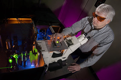
    Sandia researcher Carl Hayden

    Sandia researcher Carl Hayden positions a sample on the spectrally resolved, confocal imaging microscope.
    How to form lipid nanotubes, simply and easily

    ALBUQUERQUE, N.M. — Recent findings by medical researchers indicate that naturally occurring nanotubes may serve as tunnels that protect retroviruses and bacteria in transit from diseased to healthy cells — a fact that may explain why vaccines fare poorly against some invaders.
    To better study the missions of these intercellular nanotubes, scientists have sought the means to form them quickly and easily in test tubes.

    Sandia National Laboratories researchers have now learned serendipitously to form nanotubes with surprising ease.
    Growing nanotubes

    Growing nanotubes to examine protected passages of retroviruses
    “Our work is the first to show that the formation of nanotubes is not complicated, but can be a general effect of protein-membrane interactions alone,” says Darryl Sasaki of Sandia’s Bioscience and Energy Center.
    Sandia is a National Nuclear Security Administration laboratory.

    The tunnel-like structures have been recognized only recently as tiny but important bodily channels for the good, the bad, and the informational.

    In addition to providing protected transport to certain diseases, the nanotubes also seem to help trundle bacteria to their doom in the tentacles of microphages. Lastly, the nanotubes may provide avenues to send and receive information (in the form of chemical molecules) from cell to cell far faster than their random dispersal into the bloodstream would permit.

    Given the discovery of this radically different transportation system operating within human tissues, it was natural for researchers to attempt to duplicate the formation of the nanotubes. In their labs, they experimented with giant lipid vesicles that appeared to mimic key aspects of the cellular membrane.

    Giant lipid vesicles resemble micron-sized spherical soap bubbles that exist in water. They are composed of a lipid bilayer membrane only five nanometers thick.

    The object for experimenters was to create conditions in which the spheres would morph into cylinders of nanometer radii.

    But researchers had difficulties, says Sasaki, perhaps because they used a composite lipid called egg PC that requires unnecessarily high energies to bend into a tubular shape.

    Egg PC is inexpensive, readily available, and offers good, stable membrane properties. It is the usual lipid of choice in forming nanocylinders via mechanical stretching techniques.

    But Sandia postdoctoral researcher Haiqing Lui instead used POPC — a single pure lipid requiring half the bending energy of egg PC.

    She was trying to generate nanotubes by a completely different approach that involved the use of motor proteins to stretch naturally occurring membranes into tubes.

    Working with Sandia researcher George Bachand, she serendipitously found that interaction of the POPC membrane with a high affinity protein called streptavidin alone was enough to form the nanotubes.

    “Perhaps this information — linking membrane bending energy with nanotube formation — may provide some clue about the membrane structure and the cell’s ability to form such intercellular connections,” Sasaki says.

    The formation was confirmed by Sandia researcher Carl Hayden, who characterized the nanotube formation through a confocal imaging microscope. The custom instrument allows pixel-by-pixel examination of the protein interaction with the membranes comprising the nanotubes by detecting the spectrum and lifetimes of fluorescent labels on the proteins.

    Nanotube formation had been noticed previously by cell biologists, but they had dismissed the tiny outgrowths as “junk — an aberration of cells growing in culture,” says Sasaki. “The reason they were only noticed recently as trafficking routes is because of labeling studies that marked organelles and proteins. This allowed a focused look at what these nanostructures might be used for.”

    It became clear, says Sasaki, that the organelles were being transported with “specific directionality” on the backs of motor proteins within the tubes, rather than randomly.

    Three-dimensional networks of nanotubes also are found to be created by macrophages — part of the police force of the body — grown in culture, says George. The tubes in appearance and function resemble a kind of spider web, capturing bacterium and transporting them to the macrophages, which eat them.

    Other paper authors include postdoc Hahkjoon Kim and summer intern Elsa Abate.

    The lipid work is supported by Sandia’s Laboratory Directed Research and Development office. Motor protein work is supported by DOE’s Office of Basic Energy Sciences.

    Sandia is a multiprogram laboratory operated by Sandia Corporation, a Lockheed Martin company, for the U.S. Department of Energy’s National Nuclear Security Administration. With main facilities in Albuquerque, N.M., and Livermore, Calif., Sandia has major R&D responsibilities in national security, energy and environmental technologies, and economic competitiveness.

    Sandia news media contact: Neal Singer, DOE/Sandia National Laboratories 505-845-7078, nsinger@sandia.gov

    Monday, July 21, 2008

    LLNL researchers peer into water

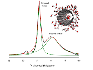
    spectrum showing features associated with water external and internal to the carbon nanotube

    An NMR spectrum showing features associated with water external and internal to the carbon nanotube (see inset). Figure by Charles Chen and Yue Wu University of North Carolina, Chapel Hill.
    LIVERMORE, Calif. – Researchers have identified a signature for water inside single-walled carbon nanotubes, helping them understand how water is structured and how it moves within these tiny channels.

    This is the first time researchers were able to get a snapshot of the water inside the carbon nanotubes.
    Single-walled carbon nanotubes (SWCNTs) offer the potential to act as a unique nanofiltration system. While experiments have demonstrated extremely fast flow in these channels, it is still unclear why, and few studies have experimentally probed the detailed structure and movement of the water within nanotubes.

    That’s where Lawrence Livermore scientists Jason Holt, Julie Herberg, and University of North Carolina’s, Yue Wu and colleagues come in.

    As described in an article appearing in the July edition of Nanoletters, they used a technique called Nuclear Magnetic Resonance (NMR) to get a glimpse of the water confined inside one-nanometer diameter SWCNTs.

    The nanotubes, special molecules made of carbon atoms in a unique arrangement, are hollow and more than 50,000 times thinner than a human hair. The confined water exhibited very different properties from that of bulk water, and this allowed it to be distinguished in the NMR spectrum.

    Carbon nanotubes have long been touted for their superior thermal, mechanical and electrical properties, but recent work suggests they can be used as nanoscale filters.

    Earlier Livermore studies have suggested that carbon nanotubes may be used for desalination and demineralization because of their small pore size and enhanced flow properties. Conventional desalination membranes are typically much less permeable and require large pressures, entailing high energy costs. However, these more permeable nanotube membranes could reduce the energy costs of desalination significantly.

    While the technology offers great promise, there still are important unanswered scientific questions.

    “There have been many predictions about how water behaves within carbon nanotubes,” said Holt, the principal investigator of the project, which is funded through LLNL’s Laboratory Directed Research and Development (LDRD). “With experiments like these, we can directly probe that water and determine how close those predictions were.”

    Founded in 1952, Lawrence Livermore National Laboratory is a national security laboratory, with a mission to ensure national security and apply science and technology to the important issues of our time. Lawrence Livermore National Laboratory is managed by Lawrence Livermore National Security, LLC for the U.S. Department of Energy's National Nuclear Security Administration.

    Contact: Anne Stark stark8@llnl.gov 925-422-9799 DOE/Lawrence Livermore National Laboratory

    Tags: or and

    Sunday, July 20, 2008

    Silicon photonic crystals key to optical cloaking, researchers say

    Harley Johnson, left, and Dong Xiao

    Harley Johnson, left, a mechanical science and engineering professor, and Dong Xiao, a postdoctoral researcher, have demonstrated an approximate cloaking effect created by concentric rings of silicon photonic crystals. Photo by L. Brian Stauffer
    CHAMPAIGN, Ill. — Now you see it, soon you might not, researchers at the University of Illinois say.

    In computer simulations, the researchers have demonstrated an approximate cloaking effect created by concentric rings of silicon photonic crystals. The mathematical proof brings scientists a step closer to a practical solution for optical cloaking.

    “This is much more than a theoretical exercise,” said Harley Johnson, a Cannon Faculty Scholar and professor of mechanical science and engineering at Illinois. “An optical cloaking device is almost within reach.”

    In October 2006, an invisibility cloak operating in the microwave region of the electromagnetic spectrum was reported by researchers at Duke University, Imperial College in London, and Sensor Metrix in San Diego.
    In their experimental demonstration, microwave cloaking was achieved through a thin coating containing an array of tiny metallic structures called ring resonators.

    To perform the same feat at much smaller wavelengths in the visible portion of the spectrum, however, would require ring resonators smaller than can be made with current technology, Johnson said. In addition, because metallic particles would absorb some of the incident light, the cloaking effect would be incomplete. Faintly outlined in the shape of the container, some of the background objects would appear dimmer than the rest.

    To avoid these problems, postdoctoral research associate Dong Xiao came up with the idea of using a coating of concentric rings of silicon photonic crystals. The width and spacing of the rings can be tailored for specific wavelengths of light.

    “When light of the correct wavelength strikes the coating, the light bends around the container and continues on its way, like water flowing around a rock,” Xiao said. “An observer sees what is behind the container, as though it isn’t there. Both the container and its contents are invisible.”

    Currently simulated in two dimensions, the cloaking concept could be extended to three dimensions, Xiao said, by replacing the concentric rings with spherical shells of silicon, separated by air or some other dielectric.

    The researchers’ optical cloaking technique is not perfect, however. “The wave fronts are slightly perturbed as they pass around the container,” said Johnson, who also is affiliated with the university’s Beckman Institute and the Frederick Seitz Materials Research Laboratory. “Because the wave fronts don’t match exactly, we refer to the technique as ‘approximate’ cloaking.”

    Xiao and Johnson’s work is highlighted in the June issue of the Materials Research Society Bulletin. The researchers describe their work in a paper published in the April 15 issue of the journal Optics Letters.

    Funding was provided by the U.S. Department of Energy.

    Editor’s note: To reach Harley Johnson, call 217-265-5468; e-mail: htj@uiuc.edu.

    Contact: James E. Kloeppel, Physical Sciences Editor. kloeppel@uiuc.edu 217-244-1073 University of Illinois at Urbana-Champaign

    Tags: or and

    Saturday, July 19, 2008

    The fight for the best quantum bit (qubit)

    quantum bit (qubit)Post Doc Henrik Ingerslev Jørgensen from the Nano-Science Center, located at the Niels Bohr Institute at the University of Copenhagen, has come an important step closer to the quantum computer. The journal Nature Physics has just published the researcher's groundbreaking discovery.
    - Our results give us, for the first time, the possibility to understand the interaction between just two electrons placed next to each other in a carbon nanotube. A groundbreaking discovery, which is fundamental for the creation of a quantum mechanical bit, a so-called quantum bit - the cornerstone of a quantum computer, explains Henrik Jørgensen, who is one of the many researchers competing on an international level to be the first to make a quantum bit in a carbon nanotube.

    The ability to produce a quantum computer is still some years ahead in the future, the implementation will, however, mean a revolution within the computer industry. This is due to the quantum mechanical computation method, which quickly will be able to solve certain complicated calculations that on an ordinary computer would take more than the lifetime of the Universe to calculate.
    Who will be the first?

    Over the past years there has been a tremendously increasing interest in developing a quantum computer within the international world of researchers. The production of a quantum computer is enormously challenging and demands development of new theories and new technologies by research-groups all over the world. Henrik Jørgensen's results have been developed in close collaboration with the Hitachi Cambridge Laboratory in England.

    Adviser and Vice-Chairman at the Nano-Science Center, Professor Poul Erik Lindelof, says - We have been studying the quantum mechanical properties of carbon nanotubes for ten years, and today we are one of the leading laboratories within this field of research. I believe Henrik Jørgensen's experimental work can prove to be just the right way forward.

    Kasper Grove Rasmussen is joint author of the article. He says - We use carbon nanotubes due to their unique electronic and material properties and not least due to the absence of disturbing magnetism from the atom nuclei which is found in certain competing materials.

    At present it is not possible to say which material will be the most suitable for the quantum computer, or who will be the first to realize a quantum bit in a carbon nanotube, but the researchers at the Nano-Science Center are a big step closer to the solution.

    For more information please contact: Henrik Ingerslev Jørgensen, mobile no.:+45 22269578, e-mail: hij@nano.ku.dk See: www.nature.com and University of Copenhagen

    Tags: or and

    Friday, July 18, 2008

    Laser surgery probe targets individual cancer cells

    Dr. Adela Ben-Yakar

    Dr. Adela Ben-Yakar, assistant professor of mechanical engineering, led the development of a 'Nano-scissors' laser that can perform extremely precise surgery. Originally from Israel, Dr. Ben-Yakar began her research four years ago at Stanford University and most recently was published in Nature magazine.
    AUSTIN, Texas–Mechanical engineering Assistant Professor Adela Ben-Yakar at The University of Texas at Austin has developed a laser "microscalpel" that destroys a single cell while leaving nearby cells intact, which could improve the precision of surgeries for cancer, epilepsy and other diseases.

    "You can remove a cell with high precision in 3-D without damaging the cells above and below it," Ben-Yakar says. "And you can see, with the same precision, what you are doing to guide your microsurgery."


    Femtosecond lasers produce extremely brief, high-energy light pulses that sear a targeted cell so quickly and accurately the lasers' heat has no time to escape and damage nearby healthy cells. As a result, the medical community envisions the lasers' use for more accurate destruction of many types of unhealthy material. These include small tumors of the vocal cords, cancer cells left behind after the removal of solid tumors, individual cancer cells scattered throughout brain or other tissue and plaque in arteries.

    A commercially available femtosecond laser system and microscope was developed recently for LASIK and other eye surgeries, but the system's bulk limits its usefulness. Ben-Yakar's laboratory has overcome technological challenges to create a microscope system that can deliver femtosecond laser pulses up to 250 microns deep inside tissue. The system includes a tiny, flexible probe that focuses light pulses to a spot size smaller than human cells.

    Ben-Yakar's experimental system and its use to destroy a single cell within layers of breast cancer cells grown in the laboratory is described in the June 23 issue of Optics Express.

    Within a few years, Ben-Yakar expects to shrink the probe's 15-millimeter diameter three-fold, so it would match endoscopes used today for laparoscopic surgery. The probe tip she has developed also could be made disposable -- for use operating on people who have infectious diseases or destroying deadly viruses and other biomaterials.

    To develop the miniature laser-surgery system, Ben-Yakar worked with co-author Olav Solgaard at Stanford University's Electrical Engineering Department to incorporate a miniaturized scanning mirror. Ben-Yakar and her graduate student Chris Hoy, another co-author, also used a novel fiber optic cable that can withstand intense light pulses traveling from an infrared, femtosecond laser. To make the intensity more manageable, they stretched the light pulses into longer, weaker pulses for traveling through the fiber. Then they used the fiber's unique properties to reconstruct the light into more intense, short light pulses before entering the tissue.

    For the study, Ben-Yakar directed laser light at breast cancer cells in three-dimensional biostructures that mimic the optical properties of breast tissue. She has since studied laboratory-grown, layered cell structures that mimic skin tissue and other tissues.

    Ben-Yakar is also investigating the use of nanoparticles to focus the light energy on targeted cells. In research published last year, she demonstrated that gold nanoparticles can function as nano-scale magnifying lenses, increasing the laser light reaching cells by at least an order of magnitude, or 10-fold.

    "If we can consistently deliver nanoparticles to cancer cells or other tissue that we want to target, we would be able to remove hundreds of unwanted cells at once using a single femtosecond laser pulse," Ben-Yakar says. "But we would still be keeping the healthy cells alive while photo-damaging just the cells we want, basically creating nanoscale holes in a tissue."

    ### Grants from the National Science Foundation and the National Institute of Health funded the research.

    To learn about a larger-scale, higher precision femtosecond laser system that Ben-Yakar uses to study nerve regeneration, go to: Contact: Adela Ben-Yakar ben-yakar@mail.utexas.edu 512-475-9280 University of Texas at Austin

    Tags: or and

    Thursday, July 17, 2008

    Discovery by UC Riverside physicists could enable development of faster computers

    Ferromagnet Semiconductor Structure

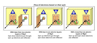
    Caption: Sketch of a ferromagnet/semiconductor structure. When the MgO interface is very thin, spin up electrons, represented in this image with an arrow to the right, are reflected back to the semiconductor. At an intermediate thickness of the interface, spin down electrons are reflected back to the semiconductor, resulting in a "spin reversal" that can be used to control current flow. Credit: Kawakami lab, UC Riverside. Usage Restrictions: None.
    Roland Kawakami's lab proposes a simple technique for controlling electron spin and current flow.

    RIVERSIDE, Calif. – Physicists at UC Riverside have made an accidental discovery in the lab that has potential to change how information in computers can be transported or stored. Dependent on the "spin" of electrons, a property electrons possess that makes them behave like tiny magnets, the discovery could help in the development of spin-based semiconductor technology such as ultrahigh-speed computers.
    The researchers were experimenting with ferromagnet/semiconductor (FM/SC) structures, which are key building blocks for semiconductor spintronic devices (microelectronic devices that perform logic operations using the spin of electrons). The FM/SC structure is sandwich-like in appearance, with the ferromagnet and semiconductor serving as microscopically thin slices between which lies a thinner still insulator made of a few atomic layers of magnesium oxide (MgO).
    Flow of Electrons Based on their Spin

    Caption: Sketch shows how the thickness of the magnesium oxide interface enables a "spin reversal" in electrons traveling through the interface. The interface is depicted as a yellow wall here. Credit: Kawakami lab, UC Riverside. Usage Restrictions: None.
    The researchers found that by simply altering the thickness of the MgO interface they were able to control which kinds of electrons, identified by spin, traveled from the semiconductor, through the interface, to the ferromagnet.

    Study results appear in the June 13 issue of Physical Review Letters.
    Experimental results:

    The spin of an electron is represented by a vector, pointing up for an Earth-like west-to-east spin; and down for an east-to-west spin. Center for Nanoscale Science and Engineering, and Li were joined by UCR's Y. Chye, Y.F. Chiang, K. Pi and W. H. Wang; and UC Santa Barbara's J.M. Stephens, S. Mack and D.D. Awschalom.

    Grants from the Office of Naval Research, the National Science Foundation and the Center for Nanoscience Innovation for Defense supported the two-year study.

    The University of California, Riverside is a doctoral research university, a living laboratory for groundbreaking exploration of issues critical to Inland Southern California, the state and communities around the world. Reflecting California's diverse culture, UCR's enrollment of about 17,000 is projected to grow to 21,000 students by 2010. The campus is planning a medical school and already has reached the heart of the Coachella Valley by way of the UCR Palm Desert Graduate Center. With an annual statewide economic impact of nearly $1 billion, UCR is actively shaping the region's future. To learn more, visit www.ucr.edu or call (951) UCR-NEWS.

    Contact: Iqbal Pittalwala iqbal@ucr.edu 951-827-6050 University of California - Riverside

    Wednesday, July 16, 2008

    Tethered molecules act as light-driven reversible nanoswitches

    Tethered Molecules Act as Light-Driven Reversible Nanoswitches

    Caption: Illustration of the light-activated switch made by the Paul Weiss lab at Penn State. A bridge within the azobenzene molecule, made by two double-bonded nitrogen atoms, each also bound to a benzene ring, reconfigures when the molecule absorbs light. The two benzene rings move to the same side of the molecule (cis configuration) when exposed to ultraviolet light, and to opposite sides (trans configuration) when exposed to visible light.

    Credit: Paul Weiss lab, Penn State. Usage Restrictions: The credit line must be published along with the image.
    Our ability to see is based on molecules in the eye that flip from one conformation to another when exposed to visible light. Now, a new technique for attaching light-sensitive organic molecules to metal surfaces allows the molecules to be switched between two different configurations in response to exposure to different wavelengths of light. Because the configuration changes are reversible and can be controlled without direct contact, this technique could enable applications that can be controlled at the molecular scale.

    The technology has been suggested as a possible basis for molecular motors, artificial muscles, and molecular electronics.
    The research results, obtained by a team led by Paul S. Weiss, distinguished professor of chemistry and physics at Penn State University and James M. Tour, Chao professor of chemistry at Rice University, are reported in the June 2008 issue of the journal Nano Letters.

    Until now, progress was impeded because, when such molecules were attached to surfaces, they no longer could be switched back and forth, as they could be when they were in solution. The new technique uses a change in the shape of an azobenzene molecule in response to light to provide two different states. The azobenzene molecule consists of a bridge of two nitrogen atoms attached to one another by a double bond, with each nitrogen atom also bound to a benzene ring. The two benzene rings can be on the same side of the molecule (cis configuration) or on opposite sides (trans configuration). When the molecule absorbs energy, in the form of light, it can change between cis and trans configurations in a process called photoisomerization. "This mechanism is essentially the same that we use in our eyes for vision," said Weiss. "The molecule responds to light by making a change that can be harnessed. In the eye, the change causes a neural impulse."

    The photoisomerization of azobenzene is understood well in solution, but the molecule must be attached to a surface in order to provide a useful molecular switch or component of a motor. Previous attempts to accomplish the switching with attached molecules were unsuccessful, either due to interactions between the molecule and the surface to which it was attached or to interferences between adjacent molecules. "To overcome the difficulty of reversible photoisomerization of molecules on surfaces, we used a carefully designed 'tether' to isolate the functional molecules from one another and from the metal surface," said Weiss. "We isolated the tethered molecules in the surrounding matrix on a self-assembled monolayer and confirmed this isolation using molecular-resolution scanning tunneling microscopy."

    When the tethered molecules were exposed to ultraviolet light in a specially built scanning tunneling microscope, they switched from the trans to the more-compact cis state. This switch was confirmed by an apparent decrease in height of the molecule above the surrounding surface. The researchers further found that exposure to visible light caused a transition back to the more-extended trans state.

    Weiss points out that this research advance is just the first step in designing a device that can be driven or actuated by such molecular change. In order to perform useful work as a switch or nanoscale-drive motor, it will be necessary to coordinate the motion of multiple molecules and to build moving parts into some sort of assembly. According to Weiss, further research by the team already has found some surprises when the molecules are lined up to work in unison, like a chorus line. ###

    This work was performed as part of the Penn State Center for Nanoscale Science, with major funding from the National Science Foundation and additional funding from the United States Department of Energy and Visionarts, Inc.

    CONTACTS: Contact: Barbara K. Kennedy science@psu.edu 891-486-34682 Penn State

    Tags: or and

    Tuesday, July 15, 2008

    A look into the nanoscale

    coherent X-ray diffraction

    Sample evolution revealed by coherent X-ray diffraction. Measured single-shot diffraction patterns at 25 ps (a ), corresponding to the object just before the laser excitation pulse, and diffraction patterns from the same object at 10 ps (b), 15 ps (c), 20 ps (d) 40 ps (e) and 140 ps ( f ) after the laser pulse.
    LIVERMORE, Calif. – Lawrence Livermore National Laboratory researchers have captured time-series snapshots of a solid as it evolves on the ultra-fast timescale.

    Using femtosecond X-ray free electron laser (FEL) pulses, the team, led by Anton Barty, is able to observe condensed phase dynamics such as crack formation, phase separation, rapid fluctuations in the liquid state or in biologically relevant environments.

    Other Livermore scientists include Michael Bogan, Stafan Hau-Riege, Stefano Marchesini, Matthias Frank, Bruce Woods, former Livermore researcher Saša Bajt and former LLNL scientist Henry Chapman, who is now at the Centre for Free Electron Laser Science, DESY, in Hamburg, Germany.

    “The ability to take images in a single shot is the key to studying non-repetitive behavior mechanisms in a sample,” Barty said.
    A visible light laser beam

    A visible light laser beam (i) is focused onto the sample (iii) and acts as the excitation pulse. A soft X-ray pulse (ii) is focused to the same location but at a continuously variable delay.

    X-ray pulse diffracts from the sample, carrying information about the transient sample structure to the CCD detector (v) in the form of a coherent diffraction pattern.

    A mirror (iv) separates the direct beam from the diffracted light: the direct FEL beam (vi) passes straight through a hole in the mirror and is not detected in the CCD image.
    As the femtosecond laser blasts the sample, it is destroyed, but not before the scientists created images with a 50-nanometer spatial resolution, and a 10-femtosecond shutter speed. (A femtosecond is one billionth of one millionth of a second. For context, a femtosecond is to a second as a second is to about 32 million years.)

    “This experiment opens the door to a new regime of time-resolved experiments in mesoscopic dynamics,” Barty said. “This technique could be extended to a few nanometers spatial and a few tens of femtoseconds temporal resolution.”

    This is the first time that optical pulses have been used to image samples at the nanometer-spatial resolution scale. Earlier studies were limited to a few micrometers.
    The “shutter speed” of the measurements is determined by the femtosecond duration of the FEL X-ray pulse. This allowed the team to obtain nanometer spatial resolution of violent and destructive events in which the sample is completely destroyed.

    The new technique is necessary to study ultrafast dynamics of non crystalline materials at nanometer-length scales.

    This includes fracture dynamics, shock formation, spallation, ablation and plasma formation under extreme conditions.

    The technique also allows researchers to image dynamic process in the solid state such as nucleation and phase growth, phase fluctuations and various forms of electronic or magnetic segregation.

    The research appears in the online edition of Nature Photonics.

    Founded in 1952, Lawrence Livermore National Laboratory is a national security laboratory, with a mission to ensure national security and apply science and technology to the important issues of our time. Lawrence Livermore National Laboratory is managed by Lawrence Livermore National Security, LLC for the U.S. Department of Energy's National Nuclear Security Administration.

    Contact: Anne Stark stark8@llnl.gov 925-422-9799 DOE/Lawrence Livermore National Laboratory

    Tags: or and