Wednesday, April 30, 2008

Attraction at the atomic level

Atomic Scale Maps of Electron Pairing in High-temperature Superconductors

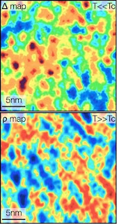
Caption: The two figures show the results obtained with a specialized scanning tunneling microscope at temperatures well above and well below when the electrons pair up in high-temperature superconductors. The top figure shows an atomic scale map of the strength (delta) for pairing of electrons while superconducting, with red showing the strongest pairing and blue the weakest. The bottom figure shows a measurement related to electron-electron interaction on the exact same atomic sites at a temperature, well above the superconducting transition temperature, when electrons repel each other. The surprising connection between these two measurements is the main finding of the paper published in Science by the team from Princeton.

Credit: Yazdani Group. Usage Restrictions: None.
Researchers find the ties that bind electrons in high-temperature superconductivity

Countless romance novels begin with a hero and heroine who initially repel each other, only to find them thrown together in uncomfortable circumstances and ultimately rejoice as their antagonism switches to ardor.

Odd as it seems, this tried-and-true romantic formula may also describe the scintillating secret behind the science of superconductivity – the phenomenon that occurs when materials conduct electricity across huge distances without losing any energy due to resistance from the transporting medium.

“It appears that the electrons with the strongest repulsion in one situation are the most adept at superconductivity in another,” said Ali Yazdani, professor of physics at Princeton University, and lead author on a paper just published in Science Magazine. “It’s counterintuitive, but that’s what’s happening.”

This research was funded by the National Science Foundation (NSF) Materials Research Science and Engineering Centers Program through the Princeton Center for Complex Materials, and by a Major Research Instrumentation Award from NSF. Additional funding came from the U.S. Department of Energy.

These research results are of fundamental importance, said NSF Program Manager Charles Bouldin. “By showing that a fundamentally different electron pairing mechanism exists in high-temperature superconductors, this work will move the field in new directions, and will help find new materials to investigate,”

Superconductivity was first discovered in 1911 in mercury when the material was cooled to the temperature of liquid helium, 4 degrees Kelvin or minus 452 degrees Fahrenheit. Scientists in later years would come to understand low-temperature superconductivity as a phenomenon that occurs when electrons interact with vibrations of the material's lattice structure and join into pairs that are able to travel through a conductor without being scattered by atoms. High-temperature superconductors such as copper oxide were discovered in 1986. They become superconducting at 150 degrees Kelvin or minus 253 degrees Fahrenheit. They can be cooled with liquid nitrogen, which is cheaper than liquid helium, making them of greater interest to industry. But do electrons bond in these materials, scientists have wondered, the same general way as in the lower temperature materials" The team with the new results says, "No."

The Princeton scientists say that high-temperature superconductivity does not hinge on a magical glue binding electrons together. The secret to superconductivity, they say, may rest instead on electrons’ ability to take advantage of their natural repulsion in a complex situation.
Having developed the ability to measure with high precision how nature allows electron pairs to form, the team, which included postdoctoral fellow Abhay Pasupathy and graduate students Aakash Pushp and Kenjiro Gomes, looked to see if there were other types of experimental signatures that could give clues to the mechanism of pairing. They found that when the samples were heated up to very high temperatures at which electrons no longer paired up, the electrons that had been superconducting at colder temperatures exhibited unique quantum properties at warmer temperatures indicating they possessed extremely strong repulsive forces.

Unlike the electrons studied in low-temperature superconducting materials, the electrons in high-temperature superconductors that are most likely to bond and flow effortlessly are the ones that repel others the strongest when the environment is not conducive to superconductivity.

The Princeton team used a specialized scanning tunneling microscope to measure with high precision how nature allows electron pairs to form. "What we have found is that the traditional signatures of what some might call the 'glue' are there – we can measure them with high accuracy on the atomic scale," Yazdani said. "They don't control the formation of the superconducting pairs, though. They are more like spectators." ###

Contact: Diane Banegas dbanegas@nsf.gov 703-292-4489 National Science Foundation

Tags: or and or and or

Tuesday, April 29, 2008

Carbon nanotubes made into conductive, flexible 'stained glass'

conductive, flexible carbon nanotube

Photograph of conductive, flexible carbon nanotube “stained glass” on flexible plastic substrates. The carbon nanotube films are arranged in order of increasing average diameter (clockwise starting from lower left): 0.9, 1.0, 1.05, 1.1, 1.4, and 1.6 nanometers. The ability to control nanotube diameter leads to the visible colors that are apparent in the photograph.
EVANSTON, Ill. --- Carbon nanotubes are promising materials for many high-technology applications due to their exceptional mechanical, thermal, chemical, optical and electrical properties.

Now researchers at Northwestern University have used metallic nanotubes to make thin films that are semitransparent, highly conductive, flexible and come in a variety of colors, with an appearance similar to stained glass. These results, published online in the journal Nano Letters, could lead to improved high-tech products such as flat-panel displays and solar cells.

The diverse and exemplary properties of carbon nanotubes have inspired a vast range of proposed applications including transistors, logic gates, interconnects, conductive films, field emission sources, infrared emitters,
biosensors, scanning probes, nanomechanical devices, mechanical reinforcements, hydrogen storage elements and catalytic supports.

Among these applications, transparent conductive films based on carbon nanotubes have attracted significant attention recently. Transparent conductors are materials that are optically transparent, yet electrically conductive. These materials are commonly utilized as electrodes in flat-panel displays, touch screens, solid-state lighting and solar cells. With pressure for energy-efficient devices and alternative energy sources increasing, the worldwide demand for transparent conductive films also is rapidly increasing.

Indium tin oxide currently is the dominant material for transparent conductive applications. However, the relative scarcity of indium coupled with growing demand has led to substantial cost increases in the past five years. In addition to this economic issue, indium tin oxide suffers from limited optical tunability and poor mechanical flexibility, which compromises its use in applications such as organic light-emitting diodes and organic photovoltaic devices.

The Northwestern team has taken an important step toward identifying an alternative transparent conductor. Utilizing a technique known as density gradient ultracentrifugation, the researchers have produced carbon nanotubes with uniform electrical and optical properties. Thin films formulated from these high purity carbon nanotubes possess 10-fold improvements in conductivity compared to pre-existing carbon nanotube materials.

In addition, density gradient ultracentrifugation allows carbon nanotubes to be sorted by their optical properties, enabling the formation of semitransparent conductive films of a given color. The resulting films thus have the appearance of stained glass. However, unlike stained glass, these carbon nanotube thin films possess high electrical conductivity and mechanical flexibility. The latter property overcomes one of the major limitations of indium tin oxide in flexible electronic and photovoltaic applications.

“Transparent conductors have become ubiquitous in modern society -- from computer monitors to cell phone displays to flat-panel televisions,” said Mark Hersam, professor of materials science and engineering in Northwestern’s McCormick School of Engineering and Applied Science and professor of chemistry in the Weinberg College of Arts and Sciences, who led the research team.

“High purity carbon nanotube thin films not only have the potential to make inroads into current applications but also accelerate the development of emerging technologies such as organic light-emitting diodes and organic photovoltaic devices. These energy-efficient and alternative energy technologies are expected to be of increasing importance in the foreseeable future.” ###

In addition to Hersam, the other author of the Nano Letters paper is Alexander Green, a graduate student in materials science and engineering at Northwestern.

Contact: Megan Fellman fellman@northwestern.edu 847-491-3115 Northwestern University

Tags: or and or and or

Monday, April 28, 2008

Manufactured Buckyballs don't harm microbes that clean the environment

researchers, from left, Larry Nies, Ron Turco and Leila Nyberg

Caption: Manufactured nanoparticles, called Buckyballs, apparently don't harm the microorganisms responsible for cleaning wastewater. Purdue researchers, from left, Larry Nies, Ron Turco and Leila Nyberg investigated effects of different amounts of Buckyballs added to sludge and found no change in how the microbes functioned. Nyberg is holding a serum bottle containing sludge similar to that used in the study. Credit: (Purdue University photo/Vincent Walter) Usage Restrictions: None.
WEST LAFAYETTE, Ind. - Even large amounts of manufactured nanoparticles, also known as Buckyballs, don't faze microscopic organisms that are charged with cleaning up the environment, according to Purdue University researchers.

In the first published study to examine Buckyball toxicity on microbes that break down organic substances in wastewater, the scientists used an amount of the nanoparticles on the microbes that was equivalent to pouring 10 pounds of talcum powder on a person. Because high amounts of even normally safe compounds, such as talcum powder, can be toxic, the microbes' resiliency to high Buckyball levels was an important finding, the Purdue investigators said.

The experiment on Buckyballs, which are carbon molecules C60, also led the scientists to develop a better method to determine the impact of nanoparticles on the microbial community.

"It's important to look at the entire microbial community when nanomaterials are introduced because the microbes are all interdependent for survival and growth," said Leila Nyberg, a doctoral student in the School of Civil Engineering and the study's lead author. "If we see a minor change in these microorganisms it could negatively impact ecosystems."

The microbes used in the study live without oxygen and also exist in subsurface soil and the stomachs of ruminant animals, such as cows and goats, where they aid digestion.
"We found no effect by any amount of C60 on the structure or the function of the microbial community over a short time," Nyberg said. "Based on what we know about the properties of C60, this is a realistic model of what would happen if high concentrations of nanoparticles were released into the environment."

The third naturally occurring pure carbon molecule known, Buckyballs are nano-sized, multiple-sided structures that look like soccer balls.

Nyberg and her colleagues Ron Turco and Larry Nies, professors of agronomy and civil engineering, respectively, report their findings in the current issue of Environmental Science and Technology.

"This is a fundamental study to assess the environmental behavior of these important manufactured nanoparticles," Turco said. "Our findings help to lay the groundwork for a larger research agenda, which includes timely risk assessment of many types of nanomaterials in different environments."

Nyberg analyzed microbes in each of three domains of a genetic tree - bacteria, archaea and eukarya - all including microorganisms that play a part in breaking down organic matter. Previously, researchers doing environmental risk assessment had not investigated organisms from the three domains in one study.

Because various microbes function at different stages in the breakdown of organic matter, studying members of each domain is essential to gauge whether C60 is altering microorganisms and their function, Nies said.

The scientists added varying Buckyball concentrations to wastewater sludge to determine if the nanoparticles affected the microbes. The highest amount of carbon molecules used was the equivalent of an average-size person being coated with about 10 pounds of talcum powder. Although a massive dose of even nontoxic substances could make someone ill, the high concentration of 50,000 mg of C60 to 1 kg of sludge didn't affect the microbes.

"Nanomaterials are certain to be released into the environment with the increased manufacture of products containing them, such as moisturizer, sunscreens and other personal care items," Nyberg said. "One way they'll get into the environment is through wastewater treatment plants."

A concern that has been expressed is that release of nanoparticles into water or soil could harm people, animals and the environment. On the other hand, Buckyballs have very low solubility in water. Water solubility usually is directly related to the extent and rate at which cells could absorb a substance, called bioavailability, which is an important factor in a chemical's toxicity.

"We added really high concentrations of the nanomaterials to these microcosms and we still didn't see any effect," Nyberg said. "Probably a lot of that is due to lack of bioavailability."

The Purdue team used two methods to determine if Buckyballs were changing how microorganisms did their jobs. One was a widely used molecular biology technique that enables scientists to analyze the genetics of an organism. The other was to measure the output of carbon dioxide and methane, two gases released as microbes degrade organic matter.

No tools exist to measure nanoparticles in the environment, so methods that Nyberg developed for assessment of their effects will be essential for further research, Nies said. The scientists still have questions about Buckyballs that will require longer-term studies than the three-month duration of this one. Future investigations of Buckyballs also would include exposing the microbes to C60 multiple times.

However, the scientists expect their next investigation will focus on nanotubes, a tube-shaped carbon nanomaterial that experts say are 100 to 1,000 times stronger than steel, Nyberg said. Because of their shape and strength, researchers are quickly finding many uses for them such as miniscule wires and electronic devices.

"Research on the effects of nanotubes is urgent because development and application of nanotubes is moving much faster than for Buckyballs," she said. "Environmental scientists have not kept up with it."

The research methods for the Buckyball assessment will be invaluable for future studies on nanomaterials, Nies said.

"If nanotubes are released into the environment, we must have a way to know how much is there because we don't have ways to extract and measure them," he said. "Leila's techniques will play a big role in investigating how nanotubes react with the microbial community."

The full name of Buckyballs is Buckminsterfullerene. Also commonly called fullerenes, these nanoparticles are named after American architect R. Buckminster Fuller who designed the geodesic dome that was once popular in modern architecture.

The other naturally occurring pure carbon molecules are graphite and diamonds. Manufacture of Buckyballs, which began in 1985, led to a Nobel Prize in chemistry. ###

The National Science Foundation provided funding for the Purdue scientists' environmental assessment.

Sources: Ron Turco, (765) 494-8077, turco@purdue.edu Larry Nies, (765) 494-8397, nies@purdue.edu Leila Nyberg, (765) 494-8397, lnyberg@purdue.edu Ag Communications: (765) 494-2722; Beth Forbes, forbes@purdue.edu
Agriculture News Page

Contact: Susan A. Steeves ssteeves@purdue.edu 765-496-7481 Purdue University

Tags: or and or and or

Sunday, April 27, 2008

Needle-size device created to track tumors, radiation dose

Babak Ziaie Shows the Prototype Wireless Device

Caption: Purdue engineer Babak Ziaie shows the prototype wireless device he has developed with doctoral student Chulwoo Son at the university's Birck Nanotechnology Center. The device fits inside a hypodermic needle to be injected into tumors to tell doctors the precise dose of radiation being received through therapy. The technology will eventually be shrunk to the size of a rice grain and also will be able to locate a tumor's exact position in real-time. Credit: (Purdue News Service photo/David Umberger) Usage Restrictions: None
WEST LAFAYETTE, Ind. - Engineers at Purdue University are creating a wireless device designed to be injected into tumors to tell doctors the precise dose of radiation received and locate the exact position of tumors during treatment.

The information would help to more effectively kill tumors, said Babak Ziaie, an associate professor in the School of Electrical and Computer Engineering and a researcher at Purdue's Birck Nanotechnology Center.

Ziaie is leading a team that has tested a prototype "wireless implantable passive micro-dosimeter" and said the device could be in clinical trials in 2010.

"Because organs and tumors shift inside the body during treatment, a new technology is needed to tell doctors the exact dosage of radiation received by a tumor," Ziaie said.

The prototype is enclosed in a glass capillary small enough to inject into a tumor with a syringe, said Ziaie, who has a dual appointment in Purdue's Weldon School of Biomedical Engineering.

Research findings are detailed in a paper appearing in the June issue of IEEE Transactions On Biomedical Engineering. The paper was written by doctoral student Chulwoo Son and Ziaie.
Whereas conventional imaging systems can provide a three-dimensional fix on a tumor's shifting position during therapy, these methods are difficult to use during radiation therapy, are costly and sometimes require X-rays, which can damage tissue when used repeatedly, Ziaie said.

The new device uses radio frequency identification, or RFID, technology, which does not emit damaging X-rays.

The device, which has no batteries and will be activated with electrical coils placed next to the patient, contains a miniature version of dosimeters worn by workers in occupations involving radioactivity. The tiny dosimeter could provide up-to-date information about the cumulative dose a tumor is receiving over time.

"It's a radiation dosimeter and a tracking device in the same capsule and will be hermetically sealed so that it will not have to be removed from the body," Ziaie said.

The same researchers in 2006 reported findings on the first such miniature device. However, the earlier prototype lacked adequate sensitivity, was too large and not suitable for easy implantation, Ziaie said.

New findings detail the development of a miniaturized and more sensitive dosimeter that can be implanted using a hypodermic needle. Researchers tested the prototype with radioactive cobalt.

The researchers have been funded by the National Science Foundation and recently received a two-year grant from the National Institutes of Health to continue the work. Over that time, the research team will work to simplify the fabrication process so that the devices could be manufactured inexpensively.

A key advantage of the technology is that it does not require intricate circuitry, which could make the device easier and less expensive to manufacture than more complex designs. The system consists of simple electronic devices called capacitors and coils.

The device has a diameter of about 2.5 millimeters, or thousandths of a meter, and is about 2 centimeters long, making it small enough to fit inside a large-diameter needle for injection with a syringe. The current size is small enough to be used in tumors, but researchers will work to shrink the device to about half a millimeter in diameter and half its current length, roughly the size of a rice grain, said Ziaie, who is working with Byunghoo Jung, a Purdue assistant professor of electrical and computer engineering. ###

The Purdue engineers also are working with researchers at the University of Texas Southwest Medical Center at Dallas. The Birck Nanotechnology Center is part of Purdue's Discovery Park

Contact: Emil Venere venere@purdue.edu 765-494-4709 Purdue University

Sources: Babak Ziaie, (765) 494-0725, bziaie@purdue.edu, Chulwoo Son: cson@purdue.edu, Byunghoo Jung, (765) 494-2866, jungb@purdue.edu

Note to Journalists: An electronic copy of the research paper is available from Emil Venere, (765) 494-4709, venere@purdue.edu. Babak Ziaie pronounces his last name Zee-Eye-Eee.

Tags: or and or and or

Saturday, April 26, 2008

Carnegie Mellon's Nadine Aubry, colleague Pushpendra Singh develop new model

Nadine Aubry

Dr. Aubry is Professor and Head of the Department of Mechanical Engineering at Carnegie Mellon University. Her awards include the Presidential Young Investigator Award from the National Science Foundation (NSF), and her election as Fellow of the American Physical Society (APS), Fellow of the American Society of Mechanical Engineers (ASME), Fellow of the American Association for the Advancement of Science (AAAS), and Senior Member of the American Institute of Aeronautics and Astronautics (AIAA).

She currently serves as Chair of the U.S. National Committee for Theoretical and Applied Mechanics (USNC/TAM) under the auspices of the National Academies. She is also a member of the Congress Committee of the International Union for Theoretical and Applied Mechanics (IUTAM) and was appointed Chair of the National Academy of Sciences (NAS) delegation to the IUTAM General Assembly. In addition, she has been serving on many APS and ASME committees, numerous NSF and National Research Council review panels and a certain number of international boards of foreign institutions.
Carnegie Mellon's Nadine Aubry, Colleague Pushpendra Singh Work To Find Method for Improved Self-Assembly of Nanoparticles

PITTSBURGH—Carnegie Mellon University's Nadine Aubry and colleague Pushpendra Singh of the New Jersey Institute of Technology (NJIT) are leading a research team to develop a manufacturing strategy that could improve technologies used in tissue engineering and information technology.

Aubry, head of Carnegie Mellon's Mechanical Engineering Department, and Singh, an engineering professor at NJIT, have developed a new way of herding nano/micro-particles into highly ordered two-dimensional lattices (monolayers) with adjustable spacing between the particles.

The team's research, reported last month in the Proceedings of the National Academy of Sciences USA journal, shows how the use of electric fields and fluid- fluid interfaces can be judiciously used to develop new materials with special properties to increase the efficiency of drug delivery patches, solar cells and the next generation of high-performance computing.

"This new manufacturing strategy could revolutionize the way we design two-dimensional nanomaterials with adaptable microscopic structures and desired properties," said Aubry, who was recently named a fellow of the American Association for the Advancement of Science (AAAS) for her outstanding contributions to the field of fluid dynamics.

The research team found they could control the particle distribution, particularly uncharged particles, at a fluid-fluid interface by applying an electric field. Without an electric field, particles self assemble. But they self assemble under capillary action, which make particles attract one another at the free-surface of a liquid. This is the same action we experience when our cereal flakes regroup at the surface of a bowl of milk.

This self-assembly via capillary action has serious flaws. Some of those flaws include an inability to manipulate small-sized particles and adjust the porosity of the resulting material. There are also inherent defects in the particle patterns.

"What is fascinating, is that the presence of an electric field can remedy all these deficiencies," Aubry said.
"The key is that when we apply the electric field, we can expand or shrink the lattice, and we can do it dynamically. The explanation is all in the subtle interplay between the forces — both electrostatic and hydrodynamic — acting on the particles."

The research team shows that their new technique creates forces capable of assembling micron-sized particles and theoretically predicts that the method should apply to nanoparticles as well.

"We are extremely excited about the new self-assembly method because it offers flexibility, precision and simplicity," Aubry said. ###

Contact: Chriss SWaney swaney@andrew.cmu.edu 412-268-5776 Carnegie Mellon University

About Carnegie Mellon: Carnegie Mellon is a private research university with a distinctive mix of programs in engineering, computer science, robotics, business, public policy, fine arts and the humanities. More than 10,000 undergraduate and graduate students receive an education characterized by its focus on creating and implementing solutions for real problems, interdisciplinary collaboration and innovation.

A small student-to-faculty ratio provides an opportunity for close interaction between the students and professors. While technology is pervasive on its 144-acre Pittsburgh campus, Carnegie Mellon is also distinctive among leading research universities for the world-renowned programs in its College of Fine Arts. A global university, Carnegie Mellon has campuses in Silicon Valley, Calif., and Qatar, and programs in Asia, Australia and Europe. For more, see www.cmu.edu.

Tags: or and or and or

Friday, April 25, 2008

Physicists saved from drowning in complexities of wetting theory

understanding the deposition of pesticides on plant leavesThe relationship between a thin liquid film or drop of liquid and the shape of the surface that it wets is explained with a new simplified mathematical formula published this week in Physical Review Letters.

Understanding the precise interaction between liquids and surfaces is important for a number of areas, including the chemical industry and new nanotechnologies.

A mathematical formula is used to explain how the relationship between the liquid and the surface changes as one wets the other. Previous formulas have all failed to explain what scientists found when they conducted experiments in this field, and have become increasingly complicated and technical.
Professor Andrew Parry from Imperial College London's Department of Mathematics, author of the new paper, has devised and tested a new way to explain this process. His formula takes into account fluctuations in the drop of liquid between the solid surface it sits on and the air above it, which have not been included in any previous formula.

"Previous descriptions have all ignored or misrepresented these interactions and consequently were at odds with experimental results and computer simulations. The new formulation appears to explain all these outstanding problems in a very elegant manner," said Professor Parry.

The study of wetting focuses on the process by which a liquid makes a surface completely wet, such as occurs if a glass of water is poured over a glass surface. However, liquids do not always make surfaces completely wet, and droplets can form on the surface, such as when water is poured on a waxy material.

Scientists know that if the temperature increases these droplets can gradually flatten out, until the surface is completely wet, and is an example of a phase transition. Exactly how this transition to complete wetting takes place has been contested by physicists for 25 years.

Wetting is of key importance in many applications ranging from oil recovery and the way pesticides are deposited on plant leaves, to inkjet printing.

Professor Parry has been working on this problem for four years, and this paper is the final one in a series of three publications addressing this problem. Previously he devised the new mathematical model and now in this most recent publication he has proven that it works. -Ends-

Contact: danielle.reeves@imperial.ac.uk danielle.reeves@imperial.ac.uk 44-020-759-42198 Imperial College London

Notes to Editors:

1. '3D Short-RangeWetting and Nonlocality,' PRL, volume 100, issue 13, published online Friday 4 April 2008.

AO. Parry (1), C. Rascon (2), N. R. Bernardino (1), and J. M. Romero-Enrique (3).

1. Department of Mathematics, Imperial College London, London SW7 2BZ, United Kingdom
2. Departamento de Matematicas, Universidad Carlos III de Madrid, 28911 Leganes, Spain
3. Departamento de Fisica Atomica, Molecular y Nuclear, Universidad de Sevilla, 41080 Seville, Spain

2. About Imperial College London

Imperial College London - rated the world's fifth best university in the 2007 Times Higher Education Supplement University Rankings - is a science-based institution with a reputation for excellence in teaching and research that attracts 12,000 students and 6,000 staff of the highest international quality. Innovative research at the College explores the interface between science, medicine, engineering and business, delivering practical solutions that improve quality of life and the environment - underpinned by a dynamic enterprise culture.

Tags: or and or and or

Thursday, April 24, 2008

Memory in artificial atoms

Memory in artificial atoms

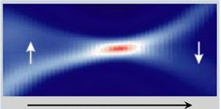
Measurement of the electrical current through the nanotube (red strong current, blue weak current). By adjusting the electrical potential to the tube, one single electron spin can be flipped. The arrows show direction of the spin.
Danish nano-physicists have made a discovery that can change the way we store data on our computers. This means that in the future we can store data much faster, and more accurate. Their discovery has been published in the esteemed scientific journal Nature Physics.

Your computer has two equally important elements: computing power and memory. Traditionally, scientists have developed these two elements in parallel. Computermemory is constructed from magnetic components, while the media of computing is electrical signals.
The discovery of the scientists at Nano-Science Center and the Niels Bohr Institute at the University of Copenhagen, Jonas Hauptmann, Jens Paaske and Poul Erik Lindelof, is a step on the way towards a new means of data-storage, in which electricity and magnetism are combined in a new transistor concept.

Jonas Hauptmann, PhD student at Nano-Science Center and the Niels Bohr Institute, has carried out the experiments under supervision of Professor Poul Erik Lindelof. Jonas Hauptmann says:

- We are the first to obtain direct electrical control of the smallest magnets in nature, one single electron spin. This has vast perspectives in the long run. In our experiments, we use carbon nanotubes as transistors. We have placed the nanotubes between magnetic electrodes and we have shown, that the direction of a single electron spin caught on the nanotube can be controlled directly by an electric potential. One can picture this single electron spin caught on the nanotube as an artificial atom.

Direct electrical control over a single electron spin has been acknowledged as a theoretical possibility for several years. Nevertheless, in spite of many zealous attempts worldwide, it is only now with this experiment that the mechanism has been demonstrated in practice. This is why the discovery of the scientists has attracted a lot of interest and has been published in the esteemed scientific journal Nature Physics.

Skou Professor at Nano-Science Center and the Niels Bohr Institute, Jens Paaske, has been in charge of the data analysis. Jens Paaske says:

- Transistors are important components in every electronic device. We work with a completely new transistor concept, in which a carbon nanotube or a single organic molecule takes the place of the traditional semi-conductor transistor. Our discovery shows that the new transistor can function as a magnetic memory.

Contact: Jonas Hauptmann jrahlf@gmail.com 452-624-2772 University of Copenhagen

Tags: or and or and or

Wednesday, April 23, 2008

Citrate appears to control buckyball clumping but environmental concerns remain

Peter Vikesland, associate professor of civil and environmental engineering at Virginia Tech.

Peter Vikesland, associate professor of civil and environmental engineering at Virginia Tech.
Blacksburg, Va. -- Fullerenes, also fondly known as buckyballs, are showing an ugly side. Since being discovered in 1985, the hollow carbon atoms have been adapted for nanotechnology and biomedical applications ranging from electronics to carriers of imaging materials.

It appears that the hydrophobic, or water hating, carbon molecules clump together in water, forming aggregates of thousands of molecules. And there are reports that these aggregates can be toxic to microorganisms and even fish, should they escape from processing into surface water and ground water.
Now researchers at Virginia Tech have demonstrated that this behavior can be changed by the addition of citric acid – although the good news and bad news of this recent discovery has yet to be determined. They will report on their research to both environmental chemists and colloidal chemists at the American Chemical Society 235th national meeting in New Orleans on April 6 to 10, 2008.

“Our group and other research groups worldwide are examining what makes these fullerene aggregates tick and how they form,” said Peter Vikesland, associate professor of civil and environmental engineering at Virginia Tech. “Once they clump, they don’t settle out. People don’t know why they remain suspended. And we don’t really know how many molecules are in a clump. We use the term nC60 where N means some number that is extremely large.”

What Vikesland’s group has done that is different and novel is, instead of mixing the molecules with water, they have added citric acid, a naturally occurring and readily available acid. “The result is that instead of unstructured clumps, we get reproducible sphere-shaped aggregates,” he said.

They discovered, for example, that in the presence of a little bit of acid, which emulates the environment in the case of an accidental release of fullerenes, the aggregates are similar to those formed in water alone. But when more acid is added, the diameter of the aggregates becomes smaller. “We want to understand the implications of this finding to the toxicity, movement, and fate of fullerenes in the environment.”

Citric acid is well understood as a proxy for other kinds of organic acids, including those within cells. Some of the citrate-based spheres that Vikesland’s group discovered are similar to what happens intercellularly when human cells are exposed to C60, he said. “We think citrate and other organic acids with a carboxyl group make C60 more water soluble.”

Vikesland will present “Effects of small molecular weight acids on C60 aggregate formation and transport (ENVR 26)” to the Division of Environmental Chemistry at 1:35 p.m. Sunday, April 6, in room 235 of the Morial convention Center. Authors of the paper are Vikesland, civil and environmental engineering Ph.D. student Xiaojun Chang of Luoyang, Henan, China, and master’s degree student Laura K. Duncan of Augusta, Ga., and research assistant professor and TEM lab director Joerg R. Jinschek

Future environmental research will be done with simulated subsurface environments using a sand column to determine how these acidified masses move in ground water.

Vikesland will present Chang’s and his research about how C60 and citric acid interact to the Division of Colloid and Surface Chemistry on Wednesday, April 9, at 4:30 p.m. in 225 Morial Convention Center. He will present the results of various imaging analysis, such as atomic force microscopy. “We have no answers but we have a hypothesis, still unproven, that there are weak interactions between citrate and individual carbon molecules that cause the spherical shape,” Vikesland said.

The Vikesland group is exploring whether the C60-citrate interaction can be used to create reproducible shaped objects. Many fullerene-based products presently require solvents, which are then washed off. Unfortunately, the engineered fullerenes can retain solvents. Using citrate “is very green chemistry,” Vikesland said. “There are no solvents. It is a cleaner way to produce these things. Citrate may be an alternative.”

But there are challenges. “It’s not a hard bond but a weak attractive force, which makes these spherical aggregates challenging to work with. At the present time we don’t know how they will fall apart and what their products are,” Vikesland said.

In the meantime, the solvent issue aside, the current rush to put fullerenes into materials may not be wise “because we don’t understand what is going on,” said Vikesland. “If you have a face cream with fullerenes as an antioxidant – we don’t know how they will react. There are many organic acids in the environment.”

He concludes, “There are uncertainties. Everyone wants to prevent future problems.” ###

Vikesland's research is supported by the National Science Foundation. The project was also supported by the Institute for Critical Technology and Applied Science at Virginia Tech.

Contact: Susan Trulove STrulove@vt.edu 540-231-5646 Virginia Tech

Tags: or and or and or

Tuesday, April 22, 2008

Hybrid computer materials may lead to faster, cheaper technology


Giovanni Vignale
A modern computer contains two different types of components: magnetic components, which perform memory functions, and semiconductor components, which perform logic operations. A University of Missouri researcher, as part of a multi-university research team, is working to combine these two functions in a single hybrid material. This new material would allow seamless integration of memory and logical functions and is expected to permit the design of devices that operate at much higher speeds and use considerably less power than current electronic devices.
Giovanni Vignale, Curators' Professor of Physics, Department of Physics and Astronomy, and expert in condensed matter physics, says the primary goal of the research team, funded by a $6.5 million grant from the Department of Defense, is to explore new ways to integrate magnetism and magnetic materials with emerging electronic materials such as organic semiconductors. The research may lead to considerably more compact and energy-efficient devices. The processing costs for these hybrid materials are projected to be much less than those of traditional semiconductor chips, resulting in devices that should be less expensive to produce.

"In this approach, the coupling between magnetic and non-magnetic components would occur via a magnetic field or flow of electron spin, which is the fundamental property of an electron and is responsible for most magnetic phenomena," Vignale said. "The hybrid devices that we target would allow seamless integration of memory and logical function, high-speed optical communication and switching, and new sensor capabilities."

Vignale studies processes by which magnetic information can be transferred from a place to another.

"One of the main theoretical tools I will be using for this project is the time-dependent, spin-current density functional theory," Vignale said. "It is a theory to which I have made many contributions over the years. The results of these theoretical calculations will be useful both to understand and to guide the experimental work of other team members."

The research grant was awarded to the University of Iowa as part of a multi-university research initiative (MURI). Vignale joins Michael Flatté (University of Iowa), Andy Kent (New York University), Yuri Suzuki (University of California, Berkeley) and Jeremy Levy (University of Pittsburgh). John Prater of the Army Research Office will monitor the program.

Links:Contact: Bryan E. Jones jonesbry@missouri.edu 573-882-9144 University of Missouri-Columbia

Tags: or and or and or

Monday, April 21, 2008

Graphene gazing gives glimpse of foundations of universe

PhD student Rahul Nair

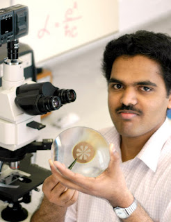
PhD student Rahul Nair (who carried out this work) shows his research sample: a scaffold in which several apertures are covered by graphene.
Researchers at The University of Manchester have used graphene to measure an important and mysterious fundamental constant - and glimpse the foundations of the universe.

The researchers from The School of Physics and Astronomy, led by Professor Andre Geim, have found that the world’s thinnest material absorbs a well-defined fraction of visible light, which allows the direct determination of the fine structure constant.

Working with Portuguese theorists from The University of Minho in Portugal, Geim and colleagues report their findings online in the latest edition of Science Express. The paper will be published in the journal Science in the coming weeks.


The universe and life on this planet are intimately controlled by several exact numbers; so-called fundamental or universal constants such as the speed of light and the electric charge of an electron.

Magnified image of research samples with small holes covered by graphene

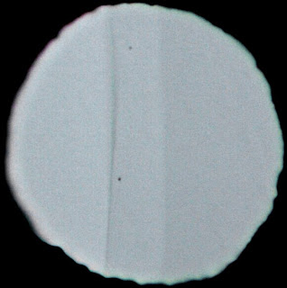
Magnified image of research samples with small holes covered by graphene. One can see light passing through them by the naked eye.
Among them, the fine structure constant is arguably most mysterious. It defines the interaction between very fast moving electrical charges and light – or electromagnetic waves – and its exact value is close to 1/137.

Prof Geim, who in 2004 discovered graphene with Dr Kostya Novoselov, a one-atom-thick gauze of carbon atoms resembling chicken wire, says: “Change this fine tuned number by only a few percent and the life would not be here because nuclear reactions in which carbon is generated from lighter elements in burning stars would be forbidden. No carbon means no life.”


Geim now working together with PhD students Rahul Nair and Peter Blake have for the first time produced large suspended membranes of graphene so that one can easily see light passing through this thinnest of all materials.

fine structure constant makes graphene visible.

The fine structure constant makes graphene visible. Looking through an aperture partially covered by graphene (central vertical stripe) and two layers of graphene (region to the right), one can directly see their different opacities. The central region absorbs 2.3 percent of incident light and the bilayer region twice more.
The researchers have found the carbon monolayer is not crystal-clear but notably opaque, absorbing a rather large 2.3 percent of visible light. The experiments supported by theory show this number divided by Pi gives you the exact value of the fine structures constant.

The fundamental reason for this is that electrons in graphene behave as if they have completely lost their mass, as shown in the previous work of the Manchester group and repeated by many researchers worldwide.

The accuracy of the optical determination of the constant so far is relatively low, by metrological standards.


But researchers say the simplicity of the Manchester experiment is “truly amazing” as measurements of fundamental constants normally require sophisticated facilities and special conditions.

With large membranes in hand, Prof Geim says it requires barely anything more sophisticated then a camera to measure visual transparency of graphene.

“We were absolutely flabbergasted when realized that such a fundamental effect could be measured in such a simple way. One can have a glimpse of the very foundations of our universe just looking through graphene,” said Prof Geim.

“Graphene continues to surprise beyond the wildest imagination of the early days when we found this material.

“It works like a magic wand – whatever property or phenomenon you address with graphene, it brings you back a sheer magic.

“I was rather pessimistic about graphene-based technologies coming out of research labs any time soon. I have to admit I was wrong. They are coming sooner rather than later.” ###

Contact: Alex Waddington alex.waddington@manchester.ac.uk Web: University of Manchester

Tags: or and or and or

Sunday, April 20, 2008

Nanosized technology has supersized effect on tumors

Tumor Blood Supply

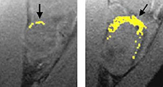
Caption: A tumor treated with fumagillin nanoparticles (left) is smaller than an untreated tumor. Nanoparticles containing an image-enhancing metal (yellow) show that the treated tumor has much less blood vessel growth than the untreated tumor. Credit: Washington University School of Medicine. Usage Restrictions: Washington University in St. Louis provides this image for free use by media for purposes of news coverage; all other uses are prohibited.
Anyone facing chemotherapy would welcome an advance promising to dramatically reduce their dose of these often harsh drugs. Using nanotechnology, researchers at Washington University School of Medicine in St. Louis have taken a step closer to that goal.

The researchers focused a powerful drug directly on tumors in rabbits using drug-coated nanoparticles. They found that a drug dose 1,000 times lower than used previously for this purpose markedly slowed tumor growth.
"Many chemotherapeutic drugs have unwanted side effects, and we've shown that our nanoparticle technology has the potential to increase drug effectiveness and decrease drug dose to alleviate harmful side effects," says lead author Patrick M. Winter, Ph.D., research assistant professor of medicine and biomedical engineering.

The nanoparticles are extremely tiny beads of an inert, oily compound that can be coated with a wide variety of active substances. In an article published online in The FASEB Journal, the researchers describe a significant reduction of tumor growth in rabbits that were treated with nanoparticles coated with a fungal toxin called fumagillin. Human clinical trials have shown that fumagillin can be an effective cancer treatment in combination with other anticancer drugs.

In addition to fumagillin, the nanoparticles' surfaces held molecules designed to stick to proteins found primarily on the cells of growing blood vessels. So the nanoparticles latched on to sites of blood vessel proliferation and released their fumagillin load into blood vessel cells. Fumagillin blocks multiplication of blood vessel cells, so it inhibited tumors from expanding their blood supply and slowed their growth.

Human trials have also shown that fumagillin can have neurotoxic side effects at the high doses required when given by standard methods. But the fumagillin nanoparticles were effective in very low doses because they concentrate where tumors create new blood vessels. The rabbits that received fumagillin nanoparticles showed no adverse side effects.

Senior author Gregory M. Lanza, M.D., Ph.D., associate professor of medicine and of biomedical engineering, and Samuel A. Wickline, M.D., professor of medicine, of physics and of biomedical engineering, are co-inventors of the nanoparticle technology. The nanoparticles measure only about 200 nanometers across, or 500 times smaller than the width of a human hair. Their cores are composed mostly of perfluorocarbon, a safe compound used in artificial blood.

The nanoparticles can be adapted to many different medical applications. In addition to carrying drugs to targeted locations, they can be manufactured to highlight specific targets in magnetic resonance imaging (MRI), nuclear imaging, CT scanning and ultrasound imaging.

In this study, researchers loaded blood-vessel-targeted nanoparticles with MRI contrast agent and were able to make detailed maps of tumor blood vessel growth using standard MRI equipment. The MRI scans showed that blood vessel formation tended to concentrate in limited areas on the surface at one side of tumors instead of dispersing uniformly, which was a surprise.

"Using the blood-vessel targeted nanoparticles, we get a far more complete view of tumor biology than we would get with any other technique," Winter says. "If you followed a tumor over a period of time with the nanoparticles and MRI scans, you would have a much better understanding of the tumor's reaction to treatment."

The researchers say they believe nanoparticle technology will be very useful for monitoring cancer treatment results in both the short and long term.

"It gives you a way of determining whether you should continue treatment, change the dose or even try a different treatment altogether," Lanza says.

Prior work has shown that the nanoparticles can be loaded with many kinds of drugs. The researchers used fumagillin nanoparticles in these experiments to demonstrate the feasibility of this approach, but they plan further investigations with other versions of the nanoparticles.

"What this report clearly demonstrates is that our nanoparticles can carry chemotherapeutic drugs specifically to tumors and have an effect at the tumor site," Lanza says. "Sometimes when I give presentations about our nanotechnology, people react as if it was science fiction or at best a technology of the distant future. But we've shown that the technology is ready for medical applications now."

The nanoparticles will be tested this year in preliminary human clinical trials to determine the optimal method for using them as imaging agents. These studies will lay essential groundwork for using the nanoparticles as therapeutic agents.

###

Winter PM, Schmieder, AH, Caruthers SD, Keene JL, Zhang H, Wickline SA, Lanza GM. Minute dosages of "v"3-targeted fumagillin nanoparticles impair Vx-2 tumor angiogenesis and development in rabbits. The FASEB Journal. March 24, 2008 (advance online publication).

The nanotechnology is owned by Barnes-Jewish Hospital and Washington University and licensed to Kereos Inc, a St. Louis-based company. Gregory M. Lanza and Samuel A. Wickline are scientific cofounders of Kereos.

Funding from the National Cancer Institute, the National Heart, Lung, and Blood Institute, the National Institute for Biomedical Imaging and Bioengineering, Philips Medical Systems and Philips Research supported this research.

Washington University School of Medicine's 2,100 employed and volunteer faculty physicians also are the medical staff of Barnes-Jewish and St. Louis Children's hospitals. The School of Medicine is one of the leading medical research, teaching and patient care institutions in the nation, currently ranked third in the nation by U.S. News & World Report. Through its affiliations with Barnes-Jewish and St. Louis Children's hospitals, the School of Medicine is linked to BJC HealthCare.

Contact: Gwen Ericson ericsong@wustl.edu 314-286-0141 Washington University School of Medicine

Tags: or and or and or

Saturday, April 19, 2008

More solid than solid: A potential hydrogen-storage compound

Hydrogen-Storage Compound

Caption: MOF-74 resembles a series of tightly packed straws comprised mostly of carbon atoms (white balls) with columns of zinc ions (blue balls) running down the walls. Heavy hydrogen molecules (green balls) adsorbed in MOF-74 pack into the tubes more densely than they would in solid form. Credit: NIST. Usage Restrictions: None.
One of the key engineering challenges to building a clean, efficient, hydrogen-powered car is how to design the fuel tank. Storing enough raw hydrogen for a reasonable driving range would require either impractically high pressures for gaseous hydrogen or extremely low temperatures for liquid hydrogen. In a new paper* researchers at the National Institute of Standards and Technology’s Center for Neutron Research (NCNR) have demonstrated that a novel class of materials could enable a practical hydrogen fuel tank.

A research team from NIST, the University of Maryland and the California Institute of Technology studied metal-organic frameworks (MOFs).
One of several classes of materials that can bind and release hydrogen under the right conditions, they have some distinct advantages over competitors. In principle they could be engineered so that refueling is as easy as pumping gas at a service station is today, and MOFs don’t require the high temperatures (110 to 500 C) some other materials need to release hydrogen.

In particular, the team examined MOF-74, a porous crystalline powder developed at the University of California at Los Angeles. MOF-74 resembles a series of tightly packed straws comprised of mostly carbon atoms with columns of zinc ions running down the inside walls. A gram of the stuff has about the same surface area as two basketball courts.

The researchers used neutron scattering and gas adsorption techniques to determine that at 77 K (-196 C), MOF-74 can adsorb more hydrogen than any unpressurized framework structure studied to date—packing the molecules in more densely than they would be if frozen in a block.

NCNR scientist Craig Brown says that, though his team doesn’t understand exactly what allows the hydrogen to bond in this fashion, they think the zinc center has some interesting properties.

“When we started doing experiments, we realized the metal interaction doesn’t just increase the temperature at which hydrogen can be stored, but it also increases the density above that in solid hydrogen,” Brown says. “This is absolutely the first time this has been encountered without having to use pressure.”

Although the liquid-nitrogen temperature of MOF-74 is not exactly temperate, it’s easier to reach than the temperature of solid hydrogen (-269 C), and one of the goals of this research is to achieve energy densities great enough to be as economical as gasoline at ambient, and thus less costly, temperatures. MOF-74 is a step forward in terms of understanding energy density, but there are other factors left to be dealt with that, once addressed, could further increase the temperature at which the fuel can be stored. Fully understanding the physics of the interaction might allow scientists to develop means for removing refrigeration or insulation, both of which are costly in terms of fuel economy, fuel production, or both. ###

The work was funded in part through the Department of Energy's Hydrogen Sorption Center of Excellence.

* Y. Liu, H. Kabbour, C.M. Brown, D.A. Neumann and C.C. Ahn. Increasing the density of adsorbed hydrogen with coordinatively unsaturated metal centers in metal-organic frameworks. Langmuir, ASAP Article 10.1021/la703864a. Published March 27, 2008.

Contact: Mark Esser mark.esser@nist.gov 301-975-2767 National Institute of Standards and Technology (NIST)

RELATED: Tags: or and or and or

Friday, April 18, 2008

Bon MOT: Innovative Atom Trap Catches Highly Magnetic Atoms

Innovative Atom Trap Catches Highly Magnetic Atoms

Title: Innovative Atom Trap Catches Highly Magnetic Atoms. Description: Trapped erbium: Color-enhanced image of a cloud of erbium atoms trapped and cooled and a narrow-line MOT using a single laser beam. The laser beam is coming down from the top of the image, which measures about 1 millimeter square. The atoms collect along the ellipse of a constant magnetic field (dashed line) where they come into resonance with the laser. A faint cloud of residual, higher temperature atoms caught in the magnetic trap can be seen as well.
A research team from the National Institute of Standards and Technology (NIST) and the University of Maryland has succeeded in cooling atoms of a rare-earth element, erbium, to within two millionths of a degree of absolute zero using a novel trapping and laser cooling technique. Their recent report* is a major step towards a capability to capture, cool and manipulate individual atoms of erbium, an element with unique optical properties that promises highly sensitive nanoscale force or magnetic sensors, as well as single-photon sources and amplifiers at telecommunications wavelengths. It also may have applications in quantum computing devices.

The strongly counterintuitive technique of “laser cooling” to slow down atoms to very low speeds—temperatures close to absolute zero—has become a platform technology of atomic physics.
Laser cooling combined with specially arranged magnetic fields—a so-called magneto-optical trap (MOT)—has enabled the creation of Bose-Einstein condensates, the capture of neutral atoms for experiments in quantum computing and ultra-precise time-keeping and spectroscopy experiments. The technique originally focused on atoms that were only weakly magnetic and had relatively simple energy structures that could be exploited for cooling, but two years ago** a NIST team showed that the far more complex energy structures of erbium, a strongly magnetic element, also could be manipulated for laser cooling.

The typical MOT uses a combination of six tuned laser beams converging on a point that is in a low magnetic field but surrounded by stronger fields. Originally, the lasers were tuned near a strong natural energy oscillation or resonance in the atom, a condition that provides efficient cooling but to only moderately low temperatures. In the new work, the research team instead used much gentler forces applied through a very weak resonance in order to bring erbium atoms to within a few millionths of a degree of absolute zero. Such weak resonances are only available in atoms with complex energy structures, and previously have been used only with a select group of non-magnetic atoms. When a strongly magnetic atom like erbium is used, the combination of strong magnetic forces and weak absorption of laser photons makes a traditional MOT unstable.

To beat this, the NIST/UM team turned classic MOT principles on their heads. Rather than shifting the laser frequency towards the red end of the spectrum—to impact fast, high-temperature atoms more than slow, cold ones—they shifted the laser towards the blue side to take advantage of the effects of the magnetic field on the highly magnetic erbium. Magnetism holds the atoms stably trapped while the lasers gently pushed them against the field, all the while extracting energy and cooling them. The delicate balancing act not only cools and traps the elusive erbium atoms, it does it more efficiently. The team’s modified trap design uses only a single laser and can cool erbium atoms to within two millionths of a degree of absolute zero. By contrast, a conventional MOT only brings rubidium atoms to about one ten-thousandth of a degree.

Erbium commonly is used in optical communications components for its convenient magneto-optical properties. The new trapping technique raises the possibility of using erbium and similar lanthanide elements for unique nanoscale magnetic field detectors, atomic resolution metrology, optical computing systems and quantum computing.

* A.J. Berglund, J.L. Hanssen and J.J. McClelland. Narrow-line magneto-optical cooling and trapping of strongly magnetic atoms. Physical Review Letters, V. 100, p. 113002 , March 18, 2008.

Contact: Michael Baum michael.baum@nist.gov 301-975-2763 National Institute of Standards and Technology (NIST)

Tags: or and or and or

Thursday, April 17, 2008

UCLA researchers design nanomachine that kills cancer cells

Jeffrey Zink, Ph.D.

Jeffrey Zink, Ph.D. Professor, Chemistry and Biochemistry, Inorganic Chemistry, Physical Chemistry. Member, NanoBiotechnology and Biomaterials, NanoElectronics, Photonics, Architectonics, NanoMechanical and Nanofluidic Systems, California NanoSystems Institute. Researcher, Inorganic, Nanoscience and Materials, Physical
'Nanoimpeller' releases anticancer drugs inside of cancer cells

Researchers from the Nano Machine Center at the California NanoSystems Institute at UCLA have developed a novel type of nanomachine that can capture and store anticancer drugs inside tiny pores and release them into cancer cells in response to light.

Known as a "nanoimpeller," the device is the first light-powered nanomachine that operates inside a living cell, a development that has strong implications for cancer treatment.

UCLA researchers reported the synthesis and operation of nanoparticles containing nanoimpellers that can deliver anticancer drugs March 31 in the online edition of the nanoscience journal Small.

The study was conducted jointly by Jeffrey Zink, UCLA professor of chemistry and biochemistry, and Fuyu Tamanoi, UCLA professor of microbiology, immunology and molecular genetics and director of the signal transduction and therapeutics program at UCLA's Jonsson Comprehensive Cancer Center.
Tamanoi and Zink are two of the co-directors for the Nano Machine Center for Targeted Delivery and On-Demand Release at the California NanoSystems Institute.

Nanomechanical systems designed to trap and release molecules from pores in response to a stimulus have been the subject of intensive investigation, in large part for their potential applications in precise drug delivery. Nanomaterials suitable for this type of operation must consist of both an appropriate container and a photo-activated moving component.
Fuyu Tamanoi, Ph.D.

Fuyu Tamanoi, Ph.D. Professor and Vice Chair, Microbiology, Immunology & Molecular Genetics. Director, JCCC Signal Transduction and Therapeutics Program Area. Member, California NanoSystems Institute
To achieve this, the UCLA researchers used mesoporous silica nanoparticles and coated the interiors of the pores with azobenzene, a chemical that can oscillate between two different conformations upon light exposure. Operation of the nanoimpeller was demonstrated using a variety of human cancer cells, including colon and pancreatic cancer cells. The nanoparticles were given to human cancer cells in vitro and taken up in the dark. When light was directed at the particles, the nanoimpeller mechanism took effect and released the contents.

The pores of the particles can be loaded with cargo molecules, such as dyes or anticancer drugs. In response to light exposure, a wagging motion occurs, causing the cargo molecules to escape from the pores and attack the cell. Confocal microscopic images showed that the impeller operation can be regulated precisely by the intensity of the light, the excitation time and the specific wavelength.

"We developed a mechanism that releases small molecules in aqueous and biological environments during exposure to light," Zink said.
"The nanomachines are positioned in molecular-sized pores inside of spherical particles and function in aqueous and biological environments."

"The achievement here is gaining precise control of the amount of drugs that are released by controlling the light exposure," Tamanoi said. "Controlled release to a specific location is the key issue. And the release is only activated by where the light is shining."

"We were extremely excited to discover that the machines were taken up by the cancer cells and that they responded to the light. We observed cell killing as a result of programmed cell death," Tamanoi and Zink said.

This nanoimpeller system may open a new avenue for drug delivery under external control at specific times and locations for phototherapy. Remote-control manipulation of the machine is achieved by varying both the light intensity and the time that the particles are irradiated at the specific wavelengths at which the azobenzene impellers absorb.

"This system has potential applications for precise drug delivery and might be the next generation for novel platform for the treatment of cancers such as colon and stomach cancer," Zink and Tamanoi said. "The fact that one can operate the mechanism by remote control means that one can administer repeated small-dosage releases to achieve greater control of the drug's effect."

Tamanoi and Zink say the research represents an exciting first step in developing nanomachines for cancer therapy and that further steps are required to demonstrate actual inhibition of tumor growth. ###

The research team also includes Eunshil Choi, a graduate student in Zink's lab, and Jie Lu, a postdoctoral researcher in Tamanoi's lab.

The Nano Machine Center for Targeted Delivery and On-Demand Release is a multidisciplinary research center at the California NanoSystems Institute at UCLA. The center is co-directed by four professors who have expertise in different chemical, biological and medical disciplines.

Jeffrey Zink, professor of chemistry and biochemistry, studies mechanically, electrically and optically functional silica-based nanostructured materials; Fuyu Tamanoi, professor of microbiology, immunology and molecular genetics and director of the signal transduction and therapeutics program at UCLA's Jonsson Comprehensive Cancer Center, studies signal transduction and the development of anticancer drugs.

Dr. Andre Nel, professor of medicine and chief of the division of nanomedicine at the David Geffen School of Medicine at UCLA, is an expert on nanoparticles and their interaction with substrates at the nano/bio interface; and Fraser Stoddart, professor emeritus of chemistry and biochemistry, has pioneered the design and template-directed synthesis of supramolecular and molecular machines. The team has co-authored seven papers on the topics of light activated release, pH-activated release, anticancer drug delivery and cellular uptake mechanisms of nanoparticles.

The California NanoSystems Institute was established in 2000 as a joint enterprise between UCLA and UC Santa Barbara, with $100 million in funding from the state of California and an additional $250 million in federal research grants and industry funding. The CNSI is a multidisciplinary research institute whose mission is to encourage university collaboration with industry and enable the rapid commercialization of discoveries in nanosystems.

CNSI members at UCLA include some of the world's preeminent scientists working in five targeted areas of nanosystems-related research: renewable energy; environmental nanotechnology and nanotoxicology; nanobiotechnology and biomaterials; nanomechanical and nanofluidic systems; and nanoelectronics, photonics and architectonics. For additional information, visit California NanoSystems Institute:.

Contact: Jennifer Marcus jmarcus@cnsi.ucla.edu 310-267-4839 University of California - Los Angeles

Tags: or and or and or

Wednesday, April 16, 2008

Engineers make first 'active matrix' display using nanowires

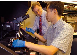
Purdue postdoctoral research associate Sanghyun Ju, sitting, and professor David B. Janes

Caption: Purdue postdoctoral research associate Sanghyun Ju, sitting, and professor David B. Janes work at a "micro-manipulation probe station" in research using nanotechnology to create transparent transistors and circuits. The innovation represents a step that promises a broad range of applications, from e-paper and flexible color screens for consumer electronics to "smart cards" and "heads-up" displays in auto windshields.

The transistors are made of single "nanowires," or tiny cylindrical structures that were assembled on glass or thin films of flexible plastic. Some of the research is being conducted at Purdue's Birck Nanotechnology Center at the university's Discovery Park. Credit: Purdue News Service photo/David Umberger. Usage Restrictions: None.
WEST LAFAYETTE, Ind. - Engineers have created the first "active matrix" display using a new class of transparent transistors and circuits, a step toward realizing applications such as e-paper, flexible color monitors and "heads-up" displays in car windshields.

The transistors are made of "nanowires," tiny cylindrical structures that are assembled on glass or thin films of flexible plastic. The researchers used nanowires as small as 20 nanometers - a thousand times thinner than a human hair - to create a display containing organic light emitting diodes, or OLEDS. The OLEDS are devices that rival the brightness of conventional pixels in flat-panel television sets, computer monitors and displays in consumer electronics.

"This is a step toward demonstrating the practical potential of nanowire transistors in displays and for other applications," said David Janes, a researcher at Purdue University's Birck Nanotechnology Center and a professor in the School of Electrical and Computer Engineering.
The nanowires were used to create a proof-of-concept active-matrix display similar to those in television sets and computer monitors. An active-matrix display is able to precisely direct the flow of electricity to produce video because each picture element, or pixel, possesses its own control circuitry.

Findings will be detailed in a research paper featured on the cover of the April issue of the journal Nano Letters. The paper was written by researchers at Purdue, Northwestern University and the University of Southern California.

"We've shown how to fabricate nanowire electronics at room temperature in a simple process that might be practical for commercial manufacturing," said Tobin J. Marks, the Vladimir N. Ipatieff Research Professor in Chemistry in Northwestern's Weinberg College of Arts and Sciences and a professor of materials science and engineering.

OLEDS are now used in cell phones and MP3 displays and prototype television sets, but their production requires a complex process, and it is difficult to manufacture OLEDs that are small enough for high-resolution displays.

"Nanowire-transistor electronics could solve this problem," said Marks, who received a 2005 National Medal of Science. "We think our fabrication method is scalable, possibly providing a low-cost way to produce high-resolution displays for many applications."

Unlike conventional computer chips - called CMOS, for complementary metal oxide semiconductor chips - the nanowire thin-film transistors could be produced less expensively under low temperatures, making them ideal to incorporate into flexible plastics that would melt under high-temperature processing.

Conventional liquid crystal displays in flat-panel televisions and monitors are backlit by a white light, and each pixel acts as a filter that turns on and off to create images. OLEDS, however, emit light directly, eliminating the need to backlight the screen and making it possible to create more vivid displays that are thin and flexible.

The technology also could be used to create antennas that aim microwave and radio signals more precisely than current antennas. Such antennas might improve cell phone reception and make it more difficult to eavesdrop on military transmissions on the battlefield.

Electronic displays like television screens contain millions of pixels located at the intersections of rows and columns that crisscross each other. In the new findings, the researchers showed that they were able to selectively illuminate a specific row of active-matrix OLEDS in a display about the size of a fingernail.

"Displays in television sets are able to illuminate a particular pixel located, say, in the 10th row, fifth column," Janes said. "We aren't able to do that yet. We've shown that we can select a whole row at a time, not a single OLED, but we're getting close."

Future research is expected to include work to design displays that can control individual OLEDs to generate images, Janes said.

"A unique aspect of these displays is that they are transparent," he said. "Until the pixels are activated, the display area looks like lightly tinted glass."

The nanowire transistors are made of a transparent semiconductor called indium oxide, a potential replacement for silicon in future transparent circuits. The OLEDS consist of the transistors, electrodes made of a material called indium tin oxide and plastic capacitors that store electricity. All of the materials are transparent until activated to emit light.

"This could enable applications such as GPS navigational displays right on the windshield of your car," Janes said. "Imagine having a local map displayed on your windshield so that you didn't have to take your eyes off the road."

The new OLEDs have a brightness nearly comparable to that of the pixels in commercial flat-panel television sets. The OLEDS have an average brightness of more than 300 candelas per square meter, compared with 400-500 candelas per square meter for commercially available liquid-crystal display televisions.

"Even in this first demonstration, we are fairly close to the brightness you'd see in an LCD television," Janes said.

The researchers also demonstrated they could create OLEDS of the proper size for commercial displays, about 176 by 54 microns, or millionths of a meter. OLEDS that size would be ideal for small displays in cell phones, personal digital assistants and other portable electronics. ###

The research has been funded by NASA through the Institute for Nanoelectronics and Computing, based at Purdue's Discovery Park.

The Nano Letters paper was authored by Sanghyun Ju, a postdoctoral research associate in Purdue's School of Electrical and Computer Engineering; doctoral students Jianfeng Li and Jun Liu at Northwestern; doctoral students Po-Chiang Chen, Hsiaokang Chang and Fumiaki Ishikawa at the University of Southern California; graduate student Young-geun Ha at Northwestern; Chongwu Zhou, an associate professor of electrical engineering at USC; Antonio Facchetti, a research associate professor in the Department of Chemistry at Northwestern University; and Marks and Janes.

Related Web sites:Contact: Emil Venere venere@purdue.edu 765-494-4709 Purdue University

Tags: or and or and or