Thursday, January 31, 2008

Researchers develop darkest manmade material

Measuring the Darkest Manmade Material

Caption: The vertically aligned carbon nanotube samples were mounted in the center of a integrating sphere, which measured the material's reflectivity. Credit: Rensselaer Usage Restrictions: Please include photo credit

Darkest Manmade Material

Caption: The new darkest manmade material, with its 0.045 percent reflectance (center), is noticeably darker than the 1.4 percent NIST reflectance standard (left) and a piece of glassy carbon. Credit: Rensselaer Usage Restrictions: Please include photo credit

SEM of Darkest Manmade Material

Caption: A side-view scanning electron micrograph of the darkest material at a high magnification. The nanotubes are vertically aligned, forming a highly porous nanostructure. Credit: Rensselaer. Usage Restrictions: Please include photo credit
Carbon nanotube array absorbs light, could boost solar energy conversion. Troy, N.Y. – Researchers at Rensselaer Polytechnic Institute and Rice University have created the darkest material ever made by man.

The material, a thin coating comprised of low-density arrays of loosely vertically-aligned carbon nanotubes, absorbs more than 99.9 percent of light and one day could be used to boost the effectiveness and efficiency of solar energy conversion, infrared sensors, and other devices. The researchers who developed the material have applied for a Guinness World Record for their efforts.

“It is a fascinating technology, and this discovery will allow us to increase the absorption efficiency of light as well as the overall radiation-to-electricity efficiency of solar energy conservation,” said Shawn-Yu Lin, professor of physics at Rensselaer and a member of the university’s Future Chips Constellation, who led the research project. “The key to this discovery was finding how to create a long, extremely porous vertically-aligned carbon nanotube array with certain surface randomness, therefore minimizing reflection and maximizing absorption simultaneously.”

The research results were published in the journal Nano Letters.

All materials, from paper to water, air, or plastic, reflect some amount of light. Scientists have long envisioned an ideal black material that absorbs all the colors of light while reflecting no light. So far they have been unsuccessful in engineering a material with a total reflectance of zero.

The total reflectance of conventional black paint, for example, is between 5 and 10 percent. The darkest manmade material, prior to the discovery by Lin’s group, boasted a total reflectance of 0.16 percent to 0.18 percent.

Lin’s team created a coating of low-density, vertically aligned carbon nanotube arrays that are engineered to have an extremely low index of refraction and the appropriate surface randomness, further reducing its reflectivity. The end result was a material with a total reflective index of 0.045 percent – more than three times darker than the previous record, which used a film deposition of nickel-phosphorous alloy.
“The loosely-packed forest of carbon nanotubes, which is full of nanoscale gaps and holes to collect and trap light, is what gives this material its unique properties,” Lin said. “Such a nanotube array not only reflects light weakly, but also absorbs light strongly. These combined features make it an ideal candidate for one day realizing a super black object.”

“The low-density aligned nanotube sample makes an ideal candidate for creating such a super dark material because it allows one to engineer the optical properties by controlling the dimensions and periodicities of the nanotubes,” said Pulickel Ajayan, the Anderson Professor of Engineering at Rice University in Houston, who worked on the project when he was a member of the Rensselaer faculty.

The research team tested the array over a broad range of visible wavelengths of light, and showed that the nanotube array’s total reflectance remains constant.

“It’s also interesting to note that the reflectance of our nanotube array is two orders of magnitude lower than that of the glassy carbon, which is remarkable because both samples are made up of the same element – carbon,” said Lin.

This discovery could lead to applications in areas such as solar energy conversion, thermalphotovoltaic electricity generation, infrared detection, and astronomical observation.

Other researchers contributing to this project and listed authors of the paper include Rensselaer physics graduate student Zu-Po Yang; Rice postdoctoral research associate Lijie Ci; and Rensselaer senior research scientist James Bur.

The project was funded by the U.S. Department of Energy’s Office of Basic Energy Sciences and the Focus Center New York for Interconnects.

Lin’s research was conducted as part of the Future Chips Constellation at Rensselaer, which focuses on innovations in materials and devices, in solid state and smart lighting, and applications such as sensing, communications, and biotechnology. A new concept in academia, Rensselaer constellations are led by outstanding faculty in fields of strategic importance. Each constellation is focused on a specific research area and comprises a multidisciplinary mix of senior and junior faculty, as well as postdoctoral researchers and graduate students. ###

About Rensselaer: Rensselaer Polytechnic Institute, founded in 1824, is the nation’s oldest technological university. The university offers bachelor’s, master’s, and doctoral degrees in engineering, the sciences, information technology, architecture, management, and the humanities and social sciences. Institute programs serve undergraduates, graduate students, and working professionals around the world.

Rensselaer faculty are known for pre-eminence in research conducted in a wide range of fields, with particular emphasis in biotechnology, nanotechnology, information technology, and the media arts and technology. The Institute is well known for its success in the transfer of technology from the laboratory to the marketplace so that new discoveries and inventions benefit human life, protect the environment, and strengthen economic development.

Contact: Michael Mullaney mullam@rpi.edu 518-276-6161 Rensselaer Polytechnic Institute

Technorati Tags: or and or and or Republican debate Simi Valley, California 01/30/08 VIDEO and Mardi Gras Masks and In diatom, scientists find genes that may level engineering hurdle or Harriet Tubman

Wednesday, January 30, 2008

Scientists use nanotechnology to localize and control drug delivery

Genhong Cheng, professor of microbiology, immunology and molecular geneticsSystem is invisible to immune system, preventing response

Using nanotechnology, scientists from UCLA and Northwestern University have developed a localized and controlled drug delivery method that is invisible to the immune system, a discovery that could provide newer and more effective treatments for cancer and other diseases.

The study, published Jan. 22, 2008 in the journal ACS Nano, provides an example of the enormous potential and clinical significance that nanomaterials may represent in such fields as oncology, endocrinology and cardiology.
The researchers used nanoscale polymer films, about four nanometers per layer, to build a sort of matrix or platform to hold and slowly release an anti-inflammatory drug. The films are orders of magnitude thinner than conventional drug deliver coatings, said Genhong Cheng, a researcher at UCLA’s Jonsson Comprehensive Cancer Center and one of the study’s authors. A nanometer is one billionth of a meter.

“Using this system, drugs could be released slowly and under control for weeks or longer,” said Cheng, a professor of microbiology, immunology and molecular genetics. “A drug that is given orally or through the bloodstream travels throughout the system and dissipates from the body much more quickly. Using a more localized and controlled approach could limit side effects, particularly with chemotherapy drugs.”

Researchers coated tiny chips with layers of the nanoscale polymer films, which are inert and helped provide a Harry Potter-like invisibility cloak for the chips, hiding them from the body’s natural defenses. They then added Dexamethasone, an anti-inflammatory drug, between the layers. The chips were implanted in mice, and researchers found that the Dexamethasone-coated films suppressed the expression of cytokines, proteins released by the cells of the immune system to initiate a response to a foreign invader. Mice without implants and those with uncoated implants were studied to compare immune response.

The uncoated implants generated an inflammatory response from the surrounding tissue, which ultimately would have led to the body’s rejection of the implant and the breakdown of its functionality. However, tissue from the mice without implants and the mice with the nano-cloaked implants were virtually identical, proving that the film-coated implants were effectively shielded from the body’s defense system, said Edward Chow, a former UCLA graduate student who participated in the study and is one of its authors.

“The polymer films provided a cloak of invisibility for the implants, keeping the immune system from attacking,” Chow said.

The nanomaterial technology serves as a non-invasive and biocompatible platform for the delivery of a broad range of therapeutics, said Dean Ho, an assistant professor of biomedical and mechanical engineering with the McCormick School of Engineering and Applied Science, a member of the Robert H. Lurie Comprehensive Cancer Center of Northwestern University and the study’s senior author.

The technology also may prove to be an effective approach for delivering multiple drugs, controlling the sequence of multi-drug delivery strategies and enhancing the life spans of commonly implanted devises such as cardiac stents, pacemakers and continuous glucose monitors.

“For chemotherapy, this system could enhance treatment efficacy while preventing uncontrolled delivery and the resultant patient side effects,” Ho said. “Furthermore, as implantable devices continue to find widespread application in cardiovascular medicine, neural disorders and diabetes, the nano-cloaking capabilities can serve as a widely applicable approach to enhance the lifetime of these devices. This would eliminate unnecessary surgeries and enhance the efficiency of patient care.”

Many cancer drugs, chemotherapies for example, are delivered systemically through the blood stream. The drugs attack cancer cells, but also other fast growing cells causing side effects such as anemia, nausea and hair loss. If the chemotherapy could be delivered by implant directly to the tumor site, such side effects would be limited, said Cheng, who also is a member of the Center for Cell Control at the UCLA Henry Samueli School of Engineering and Applied Sciences.

“Say you have a localized cancer such as breast cancer, the drugs we give are not directly targeted to the breast,” Cheng said. “If we could apply the treatment locally and control the release of the drugs, the therapy might be more effective in treating the cancer.”

Chemotherapy drugs could potentially be placed in high concentration between the polymer films and an implant placed at the tumor site. The drugs would be released slowly, over time, delivering more of the toxic chemicals directly to the cancer cells.

This study provided the proof of principle that implants in animal models could be coated with materials that made them invisible to the immune system. Cheng and Ho are now testing in animal models whether cancer therapies can be effectively and safely administered and locally delivered using the nanomaterials.

The study was funded by the Center for Cell Control and Northwestern University, with additional support from the Jonsson Cancer Center, National Institute of Allergy and Infectious Disease of the National Institutes of Health and the V Foundation for Cancer Research. The Center for Cell Control (centerforcellcontrol.org/) is one of the Nanomedicine Development Centers funded by the National Institutes of Health through the Roadmap for Medical Research.

UCLA's Jonsson Comprehensive Cancer Center comprises about 235 researchers and clinicians engaged in disease research, prevention, detection, control, treatment and education. One of the nation's largest comprehensive cancer centers, the Jonsson center is dedicated to promoting research and translating basic science into leading-edge clinical studies. In July 2007, the Jonsson Cancer Center was named the best cancer center in California by U.S. News & World Report, a ranking it has held for eight consecutive years. For more information on the Jonsson Cancer Center, visit our Web site at cancer.mednet.ucla.edu/.

Contact: Kim Irwin kirwin@mednet.ucla.edu 310-206-2805 University of California - Los Angeles

Technorati Tags: or and or and or Republican debate Simi Valley, California 01/30/08 VIDEO and Mardi Gras Masks and In diatom, scientists find genes that may level engineering hurdle or Harriet Tubman

Tuesday, January 29, 2008

In diatom, scientists find genes that may level engineering hurdle

diatoms — unicellular algae

By manipulating the genes responsible for silica production in diatoms — unicellular algae that encase themselves in intricately patterned, glass-like shells — scientists hope to produce faster computer chips. Photo: courtesy Wikimedia Commons
Denizens of oceans, lakes and even wet soil, diatoms are unicellular algae that encase themselves in intricately patterned, glass-like shells. Curiously, these tiny phytoplankton could be harboring the next big breakthrough in computer chips.

Diatoms build their hard cell walls by laying down submicron-sized lines of silica, a compound related to the key material of the semiconductor industry — silicon. "If we can genetically control that process, we would have a whole new way of performing the nanofabrication used to make computer chips," says Michael Sussman, a University of Wisconsin-Madison biochemistry professor and director of the UW-Madison's Biotechnology Center.
To that end, a team led by Sussman and diatom expert Virginia Armbrust of the University of Washington has reported finding a set of 75 genes specifically involved in silica bioprocessing in the diatom Thalassiosira pseudonana, as published today in the online Early Edition of the Proceedings of the National Academy of Sciences. Armbrust, an oceanography professor who studies the ecological role of diatoms, headed up the effort to sequence the genome of T. pseudonana, which was completed in 2004.

The new data will enable Sussman to start manipulating the genes responsible for silica production and potentially harness them to produce lines on computer chips. This could vastly increase chip speed, Sussman says, because diatoms are capable of producing lines much smaller than current technology allows.

"The semiconductor industry has been able to double the density of transistors on computer chips every few years. They've been doing that using photolithographic techniques for the past 30 years," explains Sussman. "But they are actually hitting a wall now because they're getting down to the resolution of visible light."

Before diatoms were appreciated for their engineering prowess, they interested ecologists for their role in the planet's carbon cycle. These photosynthetic cells soak up carbon dioxide and then fall to the ocean floor. They account for upwards of 20 percent of the carbon dioxide that is removed from the atmosphere each year, an amount comparable to that removed by all of the planet's rainforests combined.

"We want to see which genes express under different environmental conditions because these organisms are so important in global carbon cycling," explains Thomas Mock, a postdoctoral researcher in Armbrust's lab and the paper's first author.

But research on these algae has uncovered other enticing possibilities. As he learned about diatoms, Sussman became intrigued by the fact that each species of diatom-there may be around 100,000 of them-is believed to sport a uniquely designed cell wall.

To determine which genes are involved in creating those distinctive patterns, the research team used a DNA chip developed by Sussman, UW-Madison electrical engineer Franco Cerrina and UW-Madison geneticist Fred Blattner, the three founders of the biotechnology company NimbleGen. Put simply, the chip allows scientists to see which genes are involved in a given cellular process. In this case, the chip identified genes that responded when diatoms were grown in low levels of silicic acid, the raw material they use to make silica.

Of the 30 genes that increased their expression the most during silicic acid starvation, 25 are completely new, displaying no similarities to known genes.

"Now we know which of the organism's 13,000 genes are most likely to be involved in silica bioprocessing. Now we can zero in on those top 30 genes and start genetically manipulating them and see what happens," says Sussman.

For his part, Sussman is optimistic that in the long run these findings will help him improve the DNA chip he helped develop — the very one used to gather data for this research project. "It's like the Lion King song," he says. "You know, 'the circle of life.'"

Contributions to this paper were also made by Vaughn Iverson, Chris Berthiaume, Karie Holtermann and Colleen Durkin of the University of Washington; Manoj Pratim Samanta of Systemix Institute; Matthew Robison, Sandra Splinter BonDurant, Kathryn Richmond, Matthew Rodesch, Toivo Kallas, Edward L. Huttlin and Francesco Cerrina of the University of Wisconsin-Madison.

Funding came from the Gordon and Betty Moore Foundation, the National Science Foundation, the UW National Institutes of Health Genomic Sciences Training Grant and the postdoctoral program of the German Academic Exchange Service.

Story by Nicole Miller Contact: Michael Sussman msussman@wisc.edu 608-262-8608 University of Wisconsin-Madison

Technorati Tags: or and or and or State of the Union address 2008 VIDEO and Valentine Lace Hearts and Solar Energy Technology Licensed or Harriet Tubman

Monday, January 28, 2008

Solar Energy Technology Licensed

Solar Cells Dan Gaffney: UNSW Media Office, 0411 156 015Making solar energy cheaper and more efficient is the aim of a new licensing deal between the University of California, Davis, and Q1 NanoSystems. The university and the company, based in West Sacramento, Calif., have agreed on terms for exclusive licensing of a package of jointly-owned intellectual property stemming from inventions both on and off campus.
The agreement covers inventions that enable manufacture of very thin, very small wires, films and other structures with a precise chemical makeup. The work began with inventions by Pieter Stroeve, professor of chemical engineering and materials science; postdoctoral researcher Ruxandra Vidu; Saif Islam, assistant professor of electrical and computer engineering; and graduate student Jie-Ren Ku. These discoveries were further developed in the company's labs with input from university researchers.

"Q1 is another demonstration of the quality of entrepreneurship coming out of UC Davis, thanks to growing interest from faculty, and the multiple support programs available. We're delighted to have concluded this licensing agreement with Q1," said David McGee, executive director of UC Davis InnovationAccess.

"Our understanding of nanotechnology has allowed us to use old equipment in new ways, creating advantages in manufacturing and materials performance," said Q1 NanoSystems co-founder and COO John Argo. For example, outmoded photolithography equipment, formerly used for manufacturing computer chips, can be used to produce nanoscale templates for novel structures.

The company has deep roots at UC Davis. Argo, who has an MBA from UC Davis, met some of the other co-founders at a mixer for students from the Graduate School of Management and the College of Engineering. They appeared to have a technology that was "looking for an application," Argo said.

"Q1 NanoSystems is a great example of combining the scientists' ideas with the business skills taught by our MBA program and coming up with a plan to turn those ideas into action in the marketplace," said Nicole Woolsey Biggart, dean of the Graduate School of Management at UC Davis.

John Argo and co-founders Brian Argo, Vidu and Stroeve, together with graduate student Ku, took part in the 2005 Big Bang! business plan competition organized by the management school. The team placed second.

The company has worked with both the technology-transfer and business-development units in UC Davis InnovationAccess to manage patents and licensing, and to network with potential investors and collaborators. The National Science Foundation has awarded multiple Small Business Innovation Research (SBIR) grants to the company, with the university as a subcontractor on the grant. And the company makes use of the Northern California Nanotechnology Center, a nanoscale fabrication facility located in the UC Davis College of Engineering.

"We've really enjoyed working with the university," Argo said.

About UC Davis InnovationAccess

UC Davis InnovationAccess actively manages a patent portfolio of 841 inventions reflecting the diversity of the campus's research base, and seeks opportunities to commercialize these via licensing, with 485 currently active licensees. UC Davis has also seen an upsurge in startup companies emerging from campus research and technologies, with nearly 20 companies founded since 2005. The UC Davis InnovationAccess team is comprised of more than 20 professionals with PhDs, JDs, and MBAs with significant private-sector experience.

Additional information: Contact: Andy Fell ahfell@ucdavis.edu 530-752-4533 University of California - Davis

Technorati Tags: or and or and or Freedom Calendar 01/26/08 - 02/02/08 and Captain Arthur Phillip and Penn Engineers Create Carbon Nanopipettes That Are Smaller Than Cells and Measure Electric Current or Harriet Tubman

Sunday, January 27, 2008

Scientists discover new method of observing interactions in nanoscale systems

the Heisenberg uncertainty principlethe Heisenberg uncertainty principlethe Heisenberg uncertainty principle

ATHENS, Ohio – Scientists have used new optical technologies to observe interactions in nanoscale systems that Heisenberg’s uncertainty principle usually would prohibit, according to a study published Jan. 17 in the journal Nature.

Researchers conducted experiments with high-powered lasers and quantum dots —artificial atoms that could be the building blocks of nanoscale devices for quantum communication and computing — to learn more about physics at the nanoscale.

One common phenomenon in physics is the Fano effect, which occurs when a discrete quantum state – an atom or a molecule – interacts with a continuum state of the vacuum or the host material surrounding it. The Fano effect changes the way an atom or molecule absorbs light or radiation, said Sasha Govorov, an Ohio University theoretical physicist who is co-author on the paper.

In experiments on nanoscale systems, Heisenberg’s uncertainty principle sometimes blocks scientists from observing the Fano effect, Govorov explained. The interaction of the nanoscale system and its continuum state surroundings can’t be detected.

But in a new high-resolution laser spectroscopy experiment led by M. Kroner and K. Karrai of the Center of NanoScience at the Ludwig-Maximilians University in Munich, Germany, scientists utilized a new method. They measured photons scattered from a single quantum dot while increasing the laser intensity to saturate the dot’s optical absorption. This allowed them to observe very weak interactions, signaled by the appearance of the Fano effect, for the first time.

A theory for the new nonlinear method was developed by Govorov. “Our theory suggests that the nonlinear Fano effect and the method associated with it can be potentially applied to a variety of physical systems to reveal weak interactions,” he said.

Scientists also can revisit older experiments on atoms by using modern tools such as highly coherent light sources that are strong enough to reveal such nonlinear Fano-effects, Karrai said. “We can explore new frontiers in quantum optics,” he noted. ###

The researchers were funded by the National Science Foundation (USA), SFB 631 (Germany), A. von Humboldt Foundation (Germany), Engineering and Physical Sciences Research Council (UK), SANDiE (EU), Royal Society of Edinburgh, German Excellence Initiative via the Nanosystems Initiative Munich (NIM), and Ohio University’s Nanobiotechnology Initiative.

Other co-authors on the study were S. Remi, B. Biedermann, S. Seidl and of the Ludwig-Maximilians University, W. Zhang of Ohio University; A. Badolato and P.M. Petroff of the University of California at Santa Barbara; and R. Barbour, B.D. Gerardot and R.J. Warburton of the Heriot-Watt University in Edinburgh, Scotland.

Contact: Sasha Govorov, (740) 593-9430, govorov@ohio.edu; Khaled Karrai, +49-(0)89-2877809-0, Karrai@lmu.de; Director of Research Communications Andrea Gibson, (740) 597-2166, gibsona@ohio.edu.

Contact: Andrea Gibson gibsona@ohio.edu 740-597-2166 Ohio University

A mathematical statement of Heisenberg uncertainty principle is that every quantum state has the property that the root-mean-square (RMS) deviation of the position from its mean (the standard deviation of the X-distribution):

times the RMS deviation of the momentum from its mean (the standard deviation of P):

can never be smaller than a small fixed multiple of Planck's constant:

This article is licensed under the GNU Free Documentation License. It uses material from the Wikipedia article, Uncertainty principle

Technorati Tags: or and or and or Freedom Calendar 01/26/08 - 02/02/08 and Captain Arthur Phillip and Penn Engineers Create Carbon Nanopipettes That Are Smaller Than Cells and Measure Electric Current or Harriet Tubman
Saturday, January 26, 2008

Penn Engineers Create Carbon Nanopipettes That Are Smaller Than Cells and Measure Electric Current

CNP tips buckle when pushed against the wall of a glass pipette.

CNP tips buckle when pushed against the wall of a glass pipette but instantly recover their shape. At right, a CNP penetrates through the membrane of a smooth muscle cell. Scale bars, 15 µm. (Credit: Reprinted with permission from IOP Publishing)
PHILADELPHIA –- University of Pennsylvania engineers and physicians have developed a carbon nanopipette thousands of times thinner than a human hair that measures electric current and delivers fluids into cells. Researchers developed this tiny carbon-based tool to probe cells with minimal intrusion and inject fluids without damaging or inhibiting cell growth.

Glass micropipettes are found in almost every cell laboratory in the world but are fragile at small scales, can cause irreparable cell damage and cannot be used as injectors and electrodes simultaneously. Haim Bau, a professor in the Department of Mechanical Engineering and Applied Mechanics at Penn, and his team developed tiny carbon-based pipettes that can be mass-produced to eliminate the problems associated with glass micropipettes. Although they range in size from a few tens to a few hundred nanometers, they are far stronger and more flexible than traditional glass micropipettes.
If the tip of a carbon nanopipette, or CNP, is pressed against a surface, the carbon tip bends and flexes, then recovers its initial shape. They are rigid enough to penetrate muscle cells, carcinoma cells and neurons.

Researchers believe the pipettes will be useful for concurrently measuring electrical signals of cells during fluid injection. In addition, the pipettes are transparent to X rays and electrons, making them useful when imaging even at the molecular level. Adding a functionalized protein to the pipette creates a nanoscale biosensor that can detect the presence of proteins.

“Penn’s Micro-Nano Fluidics Laboratory now mass-produces these pipettes and uses them to inject reagents into cells without damaging the cells,” Bau said. "We are ultimately interested in developing nanosurgery tools to monitor cellular processes and control or alter cellular functions. We feel CNPs will help scientists gain a better understanding of how a cell functions and help develop new drugs and therapeutics."

Just as important as the mechanical properties of carbon nanopipettes, however, is the ease of fabrication, said Michael Schrlau, a doctoral candidate and first author of the study, “Carbon Nanopipettes for Cell Probes and Intracellular Injection,” published in the most recent issue of Nanotechnology. “After depositing a carbon film inside quartz micropipettes, we wet-etch away the quartz tip to expose a carbon nanopipe. We can simultaneously produce hundreds of these integrated nanoscale devices without any complex assembly,” he said.

The next challenge for researchers is fully utilizing the new tools in nanosurgery.
"We will need to go beyond the proof-of-concept, development stage into the utilization stage," Schrlau said. "This includes finding the appropriate collaborations across engineering, life science and medical disciplines."

The research was performed by Bau and Schrlau of the School of Engineering and Applied Science at Penn and by Erica Falls and Barry Ziober of the Department of Otorhinolaryngology at the University of Pennsylvania School of Medicine.

The research was supported by an NSF-STTR grant with Vegrandis LLC and the Commonwealth of Pennsylvania through the Nano Technology Institute. ###

Contact: Jordan Reese, jreese@upenn.edu, 215-573-6604, University of Pennsylvania

Technorati Tags: or and or and or Republican debate Boca Raton, Florida 01/24/08 VIDEO and MINI (BMW) parallel Mini Coopers and Washington University, 2 industries, team to clean up mercury emissions or Booker T. Washington

Friday, January 25, 2008

Advanced Energy Consortium Will Develop Micro and NanoSensors to Boost Energy Production

University of Texas at Austin Logo

AUSTIN, Texas — The Bureau of Economic Geology at The University of Texas at Austin's Jackson School of Geosciences announces the Advanced Energy Consortium (AEC), a multimillion-dollar research consortium dedicated to the development of micro and nanotechnology applications to increase oil and gas production.

The Richard E. Smalley Institute for Nanoscale Science and Technology at Rice University, which has extensive nanotechnology expertise, will be a collaborative technical partner.

Geoscientists believe that more oil and gas can be extracted by improving their understanding of the chemical and physical characteristics of existing oil and gas reservoirs. Using current technology, typically 60 percent of oil remains underground after primary, secondary and in some cases even tertiary recovery methods.

The consortium's primary goal is to develop intelligent subsurface micro and nanosensors that can be injected into oil and gas reservoirs to help characterize the space in three dimensions and improve the recovery of existing and new hydrocarbon resources. By leveraging existing surface infrastructure, the technology will minimize environmental impact.

Members of the privately funded consortium include BP America Inc., Baker Hughes Incorporated, ConocoPhillips, Halliburton Energy Services Inc., Marathon Oil Corp., Occidental Oil and Gas, and Schlumberger. The Bureau of Economic Geology will manage the Houston-based AEC on behalf of the funding members.

The AEC will solicit leading universities and researchers worldwide for competitive project proposals and the most promising will be funded.

"The petroleum industry realizes there are exciting possibilities for the application of nanotechnologies that will provide a more comprehensive picture of existing oil and gas reserves," said Scott W. Tinker, director of the Bureau of Economic Geology. "The consortium provides a vehicle for this critical pre-competitive research and sends a great message to young people that the industry is investing substantially and for the long term."

Tinker and Jay Kipper, also of the Bureau of Economic Geology, are the AEC's managing directors.

"We look forward to working with the world's leading energy companies and oil field service firms and with Rice University as a technical partner to make this research program a success," Tinker said. "The AEC intends to kick off a series of forums starting in early 2008, bringing leading nanotechnology experts together with oil and gas exploration and production technologists. The goal is to develop a technology roadmap which will serve to more specifically target and further narrow the focus of the subsequent project solicitations."

Intelligent sensors could range from hundreds of micrometers down to hundreds of nanometers. (For reference, the human hair is about 100,000 nanometers wide.) These functional units would collect data about the physical characteristics of hydrocarbon reservoirs.

For more information, contact: J.B. Bird, The University of Texas at Austin, 512-232-9623; Jade Boyd, Rice University, 713-348-6778.

Related Sites: Contact: J.B. Bird jb.bird@mail.utexas.edu 512-232-9623 University of Texas at Austin

Technorati Tags: or and or and or Republican debate Boca Raton, Florida 01/24/08 VIDEO and MINI (BMW) parallel Mini Coopers and Washington University, 2 industries, team to clean up mercury emissions or Booker T. Washington

Thursday, January 24, 2008

Washington University, 2 industries, team to clean up mercury emissions

electric-generating plants

A Washington University environmental engineer has shown that titanium dioxide, which is found in paint solid residues from automobile manufacturing plants, can efficiently reduce mercury emissions. Pratim Biswas, Ph.D., chair of WUSTL's energy, environmental and chemical engineering department, heads a project involving Washington University, Chrysler LLC and Ameren Corporation to test a mercury removal process in a full-scale power plant.
Washington University, 2 industries, team to clean up mercury emissions, Gotcha

Washington University in St. Louis is partnering with Chrysler LLC and a major Midwest utility company in a project to determine if paint solid residues from automobile manufacturing can reduce emissions of mercury from electric power plants.

The project is based upon the technical expertise of Pratim Biswas, Ph.D., Stifel & Quinette Jens Professor of Environmental Engineering Science, who has demonstrated the effectiveness of titanium dioxide in controlling mercury in lab and recent field studies. He heads the project that will test a mercury removal process in a full-scale power plant.
The electric power industry currently is studying the use of various other chemicals to remove mercury from power plant emissions.

The U.S, government has implemented the world’s first requirements to cut mercury emissions from electric power plants.

For the past year, Chrysler has recycled dry paint solid residues from its two St. Louis assembly plants for use as an alternative fuel in Ameren Corporation’s nearby Meramec electric utility plant. Prior to this project, Chrysler’s St. Louis plants were sending one million pounds of dried paint solids to landfills each year.

Now, the paint solids replace about 570 tons of coal per year in the Ameren plant.

The paint solid residues contain titanium dioxide, which has the potential to remove mercury from coal-powered plant emissions without affecting other processes in the plant. Mercury is chemically bonded with titanium oxide, a process known as chemisorption, and thus is potentially easier to trap in the plant’s emissions scrubber system, research has found.

“Our ‘Paint to Power’ program in St. Louis is a recycling success story. Rather than filling up scarce landfill space, we are using these paint wastes to produce power for St. Louis residents and businesses,” said Deb Morrissett, Vice President of Regulatory Affairs at Chrysler. “

Now we may be able to build on that success to further protect the environment from mercury emissions,”

Biswas, who also chairs the Department of Energy, Environmental and Chemical Engineering at Washington University, and his research team have demonstrated the ability of nanostructured titanium dioxide to remove mercury with greater than 95 percent efficiency. Recently concluded tests in a pilot scale facility have further corroborated the results of the laboratory research.

“Mercury is released into the environment in trace quantities from the burning of coal in electric-generating plants,” Biswas said. “The amount of titanium dioxide in the paint solids from the Chrysler plants would be sufficient to removed the traces of mercury.”

Through its collaboration with Chrysler’s St, Louis assembly plants, Ameren’s 855-megawatt Meramec power plant is the first in the nation to generate electricity by burning paint solids recovered from an automotive manufacturing facility. In the initial phase, the project produces enough electricity to power 70 homes for a year. ###

The project has been recognized with a pollution prevention award from the St, Louis chapter of the National Association of Environmental Managers and with an Environmental Leadership Award from Chrysler.

The Washington University, Chrysler and Ameren team also received the 2007 Chrysler Environmental Leadership Award.

Contact: Tony Fitzpatrick tony_fitzpatrick@wustl.edu 31-493-552-724-851 Washington University in St. Louis

Technorati Tags: or and or and or President Bush postpones National Drug Control event after Heath Ledger death and James Meredith at the University of Mississippi and MIT gas sensor is tiny, quick or George Washington Carver

Wednesday, January 23, 2008

MIT gas sensor is tiny, quick

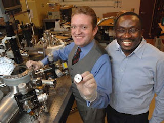
MIT research scientist Luis Velasquez-Garcia, left, and Akintunde Ibitayo Akinwande

MIT research scientist Luis Velasquez-Garcia, left, and Akintunde Ibitayo Akinwande, professor of electrical engineering and computer science, are developing a tiny sensor that can detect hazardous gases, including biochemical warfare agents. Photo / Donna Coveney
Energy-efficient device could quickly detect hazardous chemicals

Engineers at MIT are developing a tiny sensor that could be used to detect minute quantities of hazardous gases, including toxic industrial chemicals and chemical warfare agents, much more quickly than current devices.

The researchers have taken the common techniques of gas chromatography and mass spectrometry and shrunk them to fit in a device the size of a computer mouse. Eventually, the team, led by MIT Professor Akintunde Ibitayo Akinwande, plans to build a detector about the size of a matchbox.
"Everything we're doing has been done on a macro scale. We are just scaling it down," said Akinwande, a professor of electrical engineering and computer science and member of MIT's Microsystems Technology Laboratories (MTL).

Akinwande and MIT research scientist Luis Velasquez-Garcia plan to present their work at the Micro Electro Mechanical Systems (MEMS) 2008 conference next week. In December, they presented at the International Electronic Devices Meeting.

Scaling down gas detectors makes them much easier to use in a real-world environment, where they could be dispersed in a building or outdoor area. Making the devices small also reduces the amount of power they consume and enhances their sensitivity to trace amounts of gases, Akinwande said.

He is leading an international team that includes scientists from the University of Cambridge, the University of Texas at Dallas, Clean Earth Technology and Raytheon, as well as MIT.

Their detector uses gas chromatography and mass spectrometry (GC-MS) to identify gas molecules by their telltale electronic signatures. Current versions of portable GC-MS machines, which take about 15 minutes to produce results, are around 40,000 cubic centimeters, about the size of a full paper grocery bag, and use 10,000 joules of energy.

The new, smaller version consumes about four joules and produces results in about four seconds.

The device, which the researchers plan to have completed within two years, could be used to help protect water supplies or for medical diagnostics, as well as to detect hazardous gases in the air.

The analyzer works by breaking gas molecules into ionized fragments, which can be detected by their specific charge (ratio of charge to molecular weight).

Gas molecules are broken apart either by stripping electrons off the molecules, or by bombarding them with electrons stripped from carbon nanotubes. The fragments are then sent through a long, narrow electric field. At the end of the field, the ions' charges are converted to voltage and measured by an electrometer, yielding the molecules' distinctive electronic signature.

Shrinking the device greatly reduces the energy needed to power it, in part because much of the energy is dedicated to creating a vacuum in the chamber where the electric field is located.

Another advantage of the small size is that smaller systems can be precisely built using microfabrication. Also, batch-fabrication will allow the detectors to be produced inexpensively.

The research, which started three years ago, is funded by the Defense Advanced Research Projects Agency and the U.S. Army Soldier Systems Center in Natick, Mass.

A version of this article appeared in MIT Tech Talk on January 16, 2008 (download PDF).

Technorati Tags: or and or and or The Federal Open Market Committee lowers funds rate 75 basis points and 125th St. Martin Luther King Jr. Boulevard and Feeling the Heat: Berkeley Researchers Make Thermoelectric Breakthrough in Silicon Nanowires or Jack Johnson Heavyweight Champion of the World

Tuesday, January 22, 2008

Feeling the Heat: Berkeley Researchers Make Thermoelectric Breakthrough in Silicon Nanowires

Rough silicon nanowires synthesized by Berkeley Lab researchers

Rough silicon nanowires synthesized by Berkeley Lab researchers demonstrated high performance thermoelectric properties even at room temperature when connected between two suspended heating pads. In this illustration, one pad serves as the heat source (pink), the other as the sensor.
BERKELEY, CA — Energy now lost as heat during the production of electricity could be harnessed through the use of silicon nanowires synthesized via a technique developed by researchers with the U.S. Department of Energy’s (DOE) Lawrence Berkeley National Laboratory (Berkeley Lab) and the University of California (UC) at Berkeley. The far-ranging potential applications of this technology include DOE’s hydrogen fuel cell-powered “Freedom CAR,” and personal power-jackets that could use heat from the human body to recharge cell-phones and other electronic devices.

“This is the first demonstration of high performance thermoelectric capability in silicon, an abundant semiconductor for which there already exists a multibillion dollar infrastructure for low-cost and high-yield processing and packaging,” said Arun Majumdar, a mechanical engineer and materials scientist with joint appointments at Berkeley Lab and UC Berkeley, who was one of the principal investigators behind this research.
“We’ve shown that it’s possible to achieve a large enhancement of thermoelectric energy efficiency at room temperature in rough silicon nanowires that have been processed by wafer-scale electrochemical synthesis,” said chemist Peidong Yang, the other principal investigator behind this research, who also holds a joint Berkeley Lab and UC Berkeley appointment.
From left, Renkun Chen, Arun Majumdar, Peidong Yang and Allon Hochbaum

From left, Renkun Chen, Arun Majumdar, Peidong Yang and Allon Hochbaum were co-authors of a Nature paper that described a wafer-scale electrochemical synthesis technique for producing rough silicon nanowires that can convert heat into electricity with surprisingly high efficiency.
Majumdar, who was recently appointed director of Berkeley Lab's Environmental Energy Technologies Division (EETD) and is a member of the Materials Sciences Division, is an expert on energy conversion and nanoscale science and engineering. Yang is a leading nanoscience authority with Berkeley Lab's Materials Sciences Division and with the UC Berkeley Chemistry Department.

Majumdar and Yang are the co-authors of a paper appearing in the January 10, 2008 edition of the journal Nature, entitled “Enhanced Thermoelectric Performance of Rough Silicon Nanowires.” Also co-authoring this paper were Allon Hochbaum, Renkun Chen, Raul Diaz Delgado, Wenjie Liang, Erik Garnett and Mark Najarian.
The Nature paper describes a unique “electroless etching” method by which arrays of silicon nanowires are synthesized in an aqueous solution on the surfaces of wafers that can measure dozens of square inches in area. The technique involves the galvanic displacement of silicon through the reduction of silver ions on a wafer’s surface. Unlike other synthesis techniques, which yield smooth-surfaced nanowires, this electroless etching method produces arrays of vertically aligned silicon nanowires that feature exceptionally rough surfaces. The roughness is believed to be critical to the surprisingly high thermoelectric efficiency of the silicon nanowires.>


Figure (a) is a cross-sectional scanning electron microscope image of an array of rough silicon nanowires with an inset showing a typical wafer chip of these wires. Figure (b) is a transmission electron microscope image of a segment of one of these wires in which the surface roughness can be clearly seen. The inset shows that the wire is single crystalline all along its length.
“The rough surfaces are definitely playing a role in reducing the thermal conductivity of the silicon nanowires by a hundredfold, but at this time we don’t fully understand the physics,” said Majumdar. “While we cannot say exactly why it works, we can say that the technique does work.”

Nearly all of the world’s electrical power, approximately 10 trillion Watts, is generated by heat engines, giant gas or steam-powered turbines that convert heat to mechanical energy, which is then converted to electricity. Much of this heat, however, is not converted but is instead released into the environment, approximately 15 trillion Watts.
If even a small fraction of this lost heat could be converted to electricity, its impact on the energy situation would be enormous.

“Thermoelectric materials, which have the ability to convert heat into electricity, potentially could be used to capture much of the low-grade waste heat now being lost and convert it into electricity,” said Majumdar. “This would result in massive savings on fuel and carbon dioxide emissions. The same devices can also be used as refrigerators and air conditioners, and because these devices can be miniaturized, it could make heating and cooling much more localized and efficient.”

However the on-going challenge for scientists and engineers has been to make thermoelectric materials that are efficient enough to be practical. The goal is a value of 1.0 or more for a performance measurement called the “thermoelectric figure of merit” or ZT, which combines the electric and thermal conductivities of a material with its capacity to generate electricity from heat. Because these parameters are generally interdependent, attaining this goal has proven extremely difficult.

In recent years, ZT values of one or more have been achieved in thin films and nanostructures made from the semiconductor bismuth telluride and its alloys, but such materials are expensive, difficult to work with, and do not lend themselves to large-scale energy conversions.

“Bulk silicon is a poor thermoelectric material at room temperature, but by substantially reducing the thermal conductivity of our silicon nanowires without significantly reducing electrical conductivity, we have obtained ZT values of 0.60 at room temperatures in wires that were approximately 50 nanometers in diameter,” said Yang. “By reducing the diameter of the wires in combination with optimized doping and roughness control, we should be able to obtain ZT values of 1.0 or higher at room temperature.”

The ability to dip a wafer into solution and grow on its surface a forest of vertically aligned nanowires that are consistent in size opens the door to the creation of thermoelectric modules which could be used in a wide variety of situations. For example, such modules could convert the heat from automotive exhaust into supplemental power for a Freedom CAR-type vehicle, or provide the electricity a conventional vehicle needs to run its radio, air conditioner, power windows, etc.

When scaled up, thermoelectric modules could eventually be used in co-generating power with gas or steam turbines.

“You can siphon electrical power from just about any situation in which heat is being given off, heat that is currently being wasted,” said Majumdar. “For example, if it is cold outside and you are wearing a jacket made of material embedded with thermoelectric modules, you could recharge mobile electronic devices off the heat of your body. In fact, thermoelectric generators have already been used to convert body heat to power wrist watches.”

The Berkeley Lab researchers will be studying the physics behind this phenomenon to better understand and possibly manipulate it for even further improvements. They will also concentrate on the design and fabrication of thermoelectric modules based on silicon nanowire arrays. Berkeley Lab’s Technology Transfer Department is now seeking industrial partners to further develop and commercialize this technology.

This research was funded by the U.S. Department of Energy's Office of Basic Energy Science, through the Division of Materials Sciences and Engineering.

Berkeley Lab is a U.S. Department of Energy national laboratory located in Berkeley, California. It conducts unclassified scientific research and is managed by the University of California. Visit our Website at www.lbl.gov.

Contact: Lynn Yarris lcyarris@lbl.gov 510-486-5375 DOE/Lawrence Berkeley National Laboratory

Technorati Tags: or and or and or President Visits Martin Luther King, Jr., Memorial Library VIDEO PODCAST and Ebenezer Baptist Church and Nanotechnology innovation may revolutionize gene detection in a single cell

Monday, January 21, 2008

Nanotechnology innovation may revolutionize gene detection in a single cell

DNA Nanoarchitects

Caption: Lead author Yonggang Ke (left) and Hao Yan (right) are researchers in the fast-moving field known as structural DNA nanotechnology -- that assembles the molecule of life into a variety of nanostructures with a broad range of applications from human health to nanoelectronics. Yan led an interdisciplinary Arizona State University team to develop a way to use structural DNA nanotechnology to target the chemical messengers of genes, called RNA. Credit: Barb Backes. Usage Restrictions: None.

DNA Nanoarrays

Caption: On the left is an AFM image of DNA nanoarrays bound to their RNA targets at 1500nm x 1500nm scale. The zoom-in images (150nm x 150nm scale) on the right clearly show the barcode (white dots) that identifies the nanoarray and the RNA hybridization signal on the DNA nanoarray ( white bar). Credit: Yonggang Ke. Usage Restrictions: None.

DNA Origami RNA Detection Technology

Caption: By controlling the exact position and location of the chemical bases within a synthetic replica of DNA, Yan programmed a single stranded genomic DNA, M13, into nanotiles to contain the probes for specific gene expression targets. On the surface of each DNA probe tile is a dangling single stranded piece of DNA that can bind to the RNA target of interest. Each probe actually contains two half probes, so when the target RNA comes in, it will hybridize to the half probes and turn the single stranded dangling probes into a stiff structure. The group uses a powerful instrument, atomic force microscopy (AFM), which allows the researchers to image the tiles at the single molecule level. After binding to the DNA probe, the DNA-RNA hybridization becomes stiffened, it can be sensed by the atomic force microscope cantilever (blue arm), shown by bright line on the DNA tile, which is due to a height increase. The result is a mechanical, label-free detection of RNA. Credit: Hao Yan. Usage Restrictions: None.
Scientists at Arizona State University’s Biodesign Institute have developed the world’s first gene detection platform made up entirely from self-assembled DNA nanostructures. The results, appearing in the January 11 issue of the journal Science, could have broad implications for gene chip technology and may also revolutionize the way in which gene expression is analyzed in a single cell.

“We are starting with the most well-known structure in biology, DNA, and applying it as a nano-scale building material, ” said Hao Yan, a member of the institute’s Center for Single Molecule Biophysics and an assistant professor of chemistry and biochemistry in the College of Liberal and Sciences.

Yan is a researcher in the fast-moving field known as structural DNA nanotechnology — that assembles the molecule of life into a variety of nanostructures with a broad range of applications from human health to nanoelectronics.

Yan led an interdisciplinary ASU team to develop a way to use structural DNA nanotechnology to target the chemical messengers of genes, called RNA.

The team included: lead author and chemistry and biochemistry graduate student Yonggang Ke; assistant professor of chemistry and biochemistry Yan Liu; Center for Single Molecule Biophysics director and physics professor Stuart Lindsay; and associate professor in the School of Life Sciences, Yung Chang.

"This is one of the first practical applications of a powerful technology, that, till now, has mainly been the subject of research demonstrations,” said Lindsay. “The field of structural DNA nanotechnology has recently seen much exciting progress from constructing geometrical and topological nanostructures through tile based DNA self-assembly initially demonstrated by Ned Seeman, Erik Winfree and colleagues,” said Yan.

A recent breakthrough of making spatially addressable DNA nanoarrays came from Paul Rothemund’s work on scaffolded DNA origami, a method in which a long, single-stranded viral DNA scaffold can be folded and stapled by a large number of short synthetic “helper strands” into nanostructures that display complex patterns.

“But the potential of structural DNA nanotechnology in biological applications has been underestimated, and if we look at the process of DNA self-assembly, you will be amazed that trillions of DNA nanostructures can form simultaneously in a solution of few microliters, and very importantly, they are biocompatible and water soluble,” said Yan.

DNA chip and microarray technology have become a multi-billion dollar industry as scientists use it to examine thousands of genes at the same time for mutations or uncovering clues to disease. However, because DNA probes are pinned to the solid surface of the microarray chips, it is relatively slow process for the targets to search and find the probes. Also, it is hard to control the distances between the probes with nanometer accuracy.

“In this work, we developed a water soluble nanoarray that can take advantage of the DNA self-assembling process and also have benefits that the macroscopic DNA microchip arrays do not have,” said Yan. “The arrays themselves are reagents, instead of solid surface chips.”
To make the DNA origami RNA probes, Yan has taken advantage of the basic DNA pairing rules in the DNA chemical alphabet (“A” can only form a zipper-like chemical bond with “T” and “G” only pair with “C”). By controlling the exact position and location of the chemical bases within a synthetic replica of DNA, Yan programmed a single stranded genomic DNA, M13, into nanotiles to contain the probes for specific gene expression targets.

Yan refers to the self-assembled DNA nanoarrays as nucleic acid probe tiles, which look like a nanosized postage stamp. In a single step, the M13 scaffold system can churn out as many as 100 trillion of the tiles with close to100 percent yield.

Yan’s team designed three different DNA probe tiles to detect three different RNA genes along with a bar code index to tell the tiles apart from each other. “Each probe can be distinguished by its own bar code, so we mixed them together in one solution and we used this for multiplex detection,” said Yan. The group uses a powerful instrument, atomic force microscopy (AFM), which allows the researchers to image the tiles at the single molecule level.

On the surface of each DNA probe tile is a dangling single stranded piece of DNA that can bind to the RNA target of interest. “Each probe actually contains two half probes, so when the target RNA comes in, it will hybridize to the half probes and turn the single stranded dangling probes into a stiff structure,” said Yan. “When it is stiffened, it will be sensed by the atomic force microscope cantilever, and you can see a bright line, which is a height increase. The result is a mechanical, label-free detection.”

The technology is able to detect minute quantities of RNA. “Since the DNA-RNA hybridization has such a strong affinity, in principle, a single molecule would be able to hybridize to the probe tile,” said Yan.

Although there are still many technical hurdles yet to overcome, the group is excited about the potential applications of the technology. “What our approach provides is that the probe tiles are a water-soluble reagent, so the sample volume can potentially be shrunk down to the volume of a single cell level. Our ultimate goal is to detect RNA gene expression at the single cell level.” ###

Source: Hao Yan (480) 727-8570

The research was performed in the Biodesign Institute’s Center for Single Molecule Biophysics, Center for Infectious Diseases and Vaccinology, and ASU’s Department of Chemistry and Biochemistry, Department of Physics and School of Life Sciences.

This research is partly supported by funding from NIH and from NSF, U.S. Air Force Office of Scientific Research, and Office of Naval Research.

About the Biodesign Institute at ASU: The Biodesign Institute at Arizona State University is focused on innovations that improve health care; provide renewable sources of energy and clean our environment; outpace the global threat of infectious disease; and enhance national security. Using a team approach that converges the biosciences with nanoscale engineering and advanced computing, the goal is to find solutions to complex global challenges and accelerate these discoveries to market. The institute also educates future scientists by providing hands-on laboratory research for more than 250 students per semester. For more information, visit www.biodesign.asu.edu

Contact: Joe Caspermeyer joseph.caspermeyer@asu.edu 480-727-0369 Arizona State University

Technorati Tags: or and or and or Discurso Radial del Presidente a la Nación 01/19/08 and Carter G. Woodson and An “attractive” man-machine interface

Sunday, January 20, 2008

NIST reference materials are 'gold standard' for bio-nanotech research

SEM Image of Gold Nanoparticles

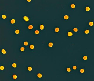
Caption: False color scanning electron micrograph (250,000 times magnification) showing the gold nanoparticles created by NIST and the National Cancer Institute's Nanotechnology Characterization Laboratory for use as reference standards in biomedical research laboratories. Credit: Andras Vladar, NIST. Usage Restrictions: None.
The National Institute of Standards and Technology (NIST) has issued its first reference standards for nanoscale particles targeted for the biomedical research community—literally “gold standards” for labs studying the biological effects of nanoparticles. The three new materials, gold spheres nominally 10, 30 and 60 nanometers in diameter, were developed in cooperation with the National Cancer Institute’s Nanotechnology Characterization Laboratory (NCL).

Nanosized particles are the subject of a great deal of biological research, in part because of concerns that in addition to having unique physical properties due to their size, they also may have unique biological properties.
On the negative side, nanoparticles may have special toxicity issues. On the positive side, they also are being studied as vehicles for targeted drug delivery that have the potential to revolutionize cancer treatments. Research in the field has suffered from a lack of reliable nanoscale measurement standards, both to ensure consistency of data from one lab to the next and to verify the performance of measurement instruments and analytic techniques.

The new NIST reference materials are citrate-stabilized nanosized gold particles in a colloidal suspension in water. They have been extensively analyzed by NIST scientists to assess particle size and size distribution by multiple techniques for dry-deposited, aerosol and liquid-borne forms of the material. Dimensions were measured using six independent methods—including atomic force microscopy (AFM), transmission electron microscopy (TEM), scanning electron microscopy (SEM), differential mobility analysis (DMA), dynamic light scattering (DLS), and small-angle X-ray scattering (SAXS). At the nanoscale in particular, different measurement techniques can and will produce different types of values for the same particles.

In addition to average size and size distributions, the new materials have been chemically analyzed for the concentrations of gold, chloride ion, sodium and citrate, as well as pH, electrical conductivity, and zeta potential (a measure of the stability of the colloidal solution). They have been sterilized with gamma radiation and tested for sterility and endotoxins. Details of the measurement procedures and data are included in a report of investigation accompanying each sample. ###

NCL examines candidate nanotech cancer drugs developed by biotech firms and academic labs. NCL and the NCI’s Alliance for Nanotechnology in Cancer sponsored the NIST work.

Additional technical and ordering information for the new NIST nanoparticle reference materials is available at:Contact: Michael Baum michael.baum@nist.gov 301-975-2763 National Institute of Standards and Technology (NIST)

Technorati Tags: or and or and or Discurso Radial del Presidente a la Nación 01/19/08 and Carter G. Woodson and An “attractive” man-machine interface