Tuesday, September 30, 2008

NPL to create 'encyclopedia for space nanomaterials'

National Physical Laboratory

Caption: National Physical Laboratory, Teddington, UK. Credit: NPL. Usage Restrictions: None.
The European Space Agency (ESA) has appointed the UK's National Physical Laboratory (NPL) to survey nanotechnology capabilities in Europe. NPL's Nanomaterials group will lead a consortium to identify the next generation of nano and smart materials that will be used in future space missions.
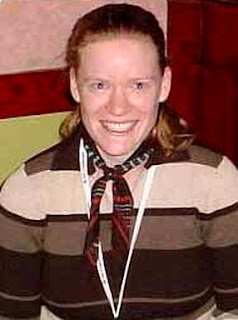
"Advances in nanotechnology are crucial to Europe's space programme," says Laurie Winkless, Higher Research Scientist in the nanomaterials group at NPL, who will be the principal author of the survey.

"The weight of spacecraft is a key factor in the overall cost of any space mission. If we can identify better, lighter and more efficient materials and the best ways of using them, it may have a huge impact on the space programme," she explains.

The NPL led consortium will help ESA to identify nanomaterials companies with potential to contribute to the future of satellite navigation and earth observation. Furthermore, it will define how these materials can add value to real space applications. High quality and thoroughly tested smart materials will play a much greater role in future applications.

The National Physical Laboratory will be joined in the consortium by specialist space consultancy ESYS and the Institute of Nanotechnology. The consortium's report is due in August 2009. It will allow ESA to review potential applications of nanomaterials for space applications and missions and quantify the resulting improvements.

Dr Constantinos Stavrinidis, Head of Mechanical Engineering at ESA explained that NPL won the contract for its long standing expertise in material science and their knowledge of the space industry.

"NPL's knowledge and experience in both areas make it a natural partner to help ESA plan the future of materials for space," he says. "By July 2009, we will know how the space programme can use nanomaterials in the next decade."

###

National Physical Laboratory

NPL is a world-leading centre of excellence in developing and applying the most accurate measurement standards, science and technology available to man.

For more than a century we have developed and maintained the nation's primary measurement standards. These standards support an infrastructure of traceable measurement through the UK and the world that ensures accuracy and consistency.

The NPL mission affects many aspects of our life. Good measurement improves productivity and quality; it underpins consumer confidence and trade, and is vital to innovation. We undertake research and share our expertise with thousands of organisations and individuals to help enhance economic performance and the quality of life.

Our services range for free technical advice, joint projects, training, secondments, problem solving, consultancy, contract research to highly accurate UKAS accredited measurement services.

The National Physical Laboratory is operated on behalf of the DIUS by NPL Management Limited, a wholly owned subsidiary of Serco Group plc.

The Institute of Nanotechnology

Established in 1997, the Institute of Nanotechnology (IoN) works closely with government, industry, and academia to provide world class information on nanotechnology developments and how these can benefit wider society.

Further information on IoN events, initiatives, and the projects we are delivering can be found at www.nano.org.uk or by contacting our head office on +44 (0)1786 458020 or Glasgow office on +44 (0)141 3038444.

The IoN is a registered Scottish Charity, No. SC025709.

ESYS

Founded in 1990, ESYS Limited originally grew out of the space and defence sector, establishing a reputation for delivering rigorous and innovative work, from initial concept through to project delivery.

Since then ESYS has extended its reach, developing a strong presence in the areas of satellite navigation, telecommunications, the environment and space research, serving a wide variety of government and commercial customers in the UK and Europe.

Today, ESYS operates with a team of consultants who are leading experts in their fields. Their knowledge and attention to detail ensures that the work of ESYS is concise, informed and accurate to allow our clients to make strategic decisions in a rapidly changing technology landscape.

The European Space Agency

The European Space Agency (ESA) and its 17 Member States work together to pursue a wide range of ambitious and exciting goals in space. Together, they create fascinating projects that would not be feasible for the individual Member States.

These projects generate new scientific knowledge and new practical applications in space exploration, and contribute to a vigorous European aerospace industry.

ESA's job is to draw up the European space programme and carry it through. ESA's programmes are designed to find out more about Earth, its immediate space environment, our Solar System and the Universe, as well as to develop satellite-based technologies and services, and to promote European industries. ESA also works closely with space organisations outside Europe.

Contact: Joe Meaney joe@proofcommunications.com 084-568-01864 National Physical Laboratory

Tags: or and

Monday, September 29, 2008

FBI unveils science of anthrax investigation

Bacillus anthracis

Caption: Bacillus anthracis spores as viewed in SEM (left) and TEM (right). Credit: Photo courtesy of Sandia National Laboratories.

Usage Restrictions: Use is allowed for educational and news-related purposes.
Sandia's work demonstrated anthrax letters contained nonweaponized form. They have worked for almost seven years in secret.

Most people did not know that the work in Ray Goehner's materials characterization department at Sandia National Laboratories was contributing important information to the FBI's investigation of letters containing bacillus anthracis, the spores that cause the disease anthrax.
The spores were mailed in the fall of 2001 to several news media offices and to two U.S. senators. Five people were killed.

Sandia's work demonstrated to the FBI that the form of bacillus anthracis contained in those letters was not a weaponized form, a form of the bacteria prepared to disperse more readily. The possibility of a weaponized form was of great concern to investigators, says Joseph Michael, the principal investigator for the project. This information was crucial in ruling out state-sponsored terrorism.
In fall of 2001, the FBI considered how to best investigate the anthrax letters. The agency convened two blue ribbon exploratory panels, and Sandia's name came up during both panels for its expertise in electron and ion microscopies and microanalysis over the range of length scales from millimeters down to nanometers. The first spore material from the letters arrived at Sandia in February of 2002.

Sandia faced some uncertainty in working on this type of investigation. Researchers signed nondisclosure agreements and agreed to make themselves available to government agencies on short notice when called to give information.

Joseph Michael, transmission electron microscopy (TEM) lab owner Paul Kotula, and a team of roughly a dozen others examined more than 200 samples in those six and a half years.
Material Characterization Analysts

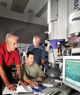
Caption: Sandia's material characterization analysts (from left to right) Joseph Michael, Paul Kotula, and manager Ray Goehner. Credit: Randy Montoya. Usage Restrictions: Use is free for educational and news-related purposes.
They received samples from the letter delivered to the New York Post, to former Sen. Tom Daschle (D-S.D.), and to Sen. Patrick Leahy (D-Vt.). The samples looked different, in part because of how the samples were prepared, which made examination initially difficult.

When bacillus anthracis spores are weaponized, the spores are coated with silica nanoparticles that look almost like lint under the microscope. The "lint" makes the particles "bouncier" and less likely to clump and fall to the ground. That makes the spores more respirable and able to do more damage, says Michael. Weaponization of the spores would be an indicator of state sponsored terrorism.

"Initially, scanning electron microscopy [SEM] conducted at another laboratory, showed high silicon and oxygen signals that led them to conclude that the spores were a weaponized form, says Kotula. "The possible misinterpretation of the SEM results arose because microanalysis in the SEM is not a surface-sensitive tool," says Kotula. "Because a spore body can be 1.5 to 2 microns wide by 1 micron long, a SEM cannot localize the elemental signal from whole spore bodies."

Using more sensitive transmission electron microscopy (TEM), Kotula and Michael's research indicated that the silica in the spore samples was not added artificially, but was incorporated as a natural part of the spore formation process. "The spores we examined," Kotula says, "lacked that fuzzy outer coating that would indicate that they'd been weaponized."

Sandia's work was the first to actually link the spore material in the New York Post, the Daschle and the Leahy letters. The elemental signatures and the locations of these signatures, while not indicating intentional weaponization, did show that the spores were indistinguishable and therefore likely came from the same source. That conclusion was corroborated a few years later by the DNA studies.

The materials characterization lab serves as a materials analysis resource for a diverse collection of projects. The lab plays an important role in stockpile surveillance, supporting Sandia's nuclear weapons mission.

Michael was recently released from his nondisclosure agreement and flown to Washington, D.C., to participate in press conferences at FBI Headquarters along with several members of research teams who'd been asked to examine other aspects of the anthrax case.

The FBI was pleased with Sandia's work, says Michael. ###

Sandia is a multiprogram laboratory operated by Sandia Corporation, a Lockheed Martin company, for the U.S. Department of Energy's National Nuclear Security Administration. With main facilities in Albuquerque, N.M., and Livermore, Calif., Sandia has major R&D responsibilities in national security, energy and environmental technologies, and economic competitiveness.

For high-res images or video, contact Sandia news media contact: Stephanie Holinka, slholin@sandia.gov, (505) 284-9227

Contact: Stephanie Holinka slholin@sandia.gov 505-284-9227 DOE/Sandia National Laboratories

Tags: or and

Sunday, September 28, 2008

Air-purifying church windows early nanotechnology

Air-Purifying Church Windows Early Nanotechnology

Caption: Associate Professor Zhu Huai Yong, from Queensland University of Technology's School of Physical and Chemical Sciences, said that church windows stained with gold paint purify the air when they are lit up by sunlight.

Credit: QUT: Erika Fish. Usage Restrictions: None.
Stained glass windows that are painted with gold purify the air when they are lit up by sunlight, a team of Queensland University of Technology experts have discovered.

Associate Professor Zhu Huai Yong, from QUT's School of Physical and Chemical Sciences said that glaziers in medieval forges were the first nanotechnologists who produced colours with gold nanoparticles of different sizes.

Professor Zhu said numerous church windows across Europe were decorated with glass coloured in gold nanoparticles.

"For centuries people appreciated only the beautiful works of art, and long life of the colours, but little did they realise that these works of art are also, in modern language, photocatalytic air purifier with nanostructured gold catalyst," Professor Zhu said.
He said tiny particles of gold, energised by the sun, were able to destroy air-borne pollutants like volatile organic chemical (VOCs), which may often come from new furniture, carpets and paint in good condition.

"These VOCs create that 'new' smell as they are slowly released from walls and furniture, but they, along with methanol and carbon monoxide, are not good for your health, even in small amounts," he said.

"Gold, when in very small particles, becomes very active under sunlight.

"The electromagnetic field of the sunlight can couple with the oscillations of the electrons in the gold particles and creates a resonance.

"The magnetic field on the surface of the gold nanoparticles can be enhanced by up to hundred times, which breaks apart the pollutant molecules in the air."

Professor Zhu said the by-product was carbon dioxide, which was comparatively safe, particularly in the small amounts that would be created through this process.

He said the use of gold nanoparticles to drive chemical reactions opened up exciting possibilities for scientific research.

"This technology is solar-powered, and is very energy efficient, because only the particles of gold heat up," he said.

"In conventional chemical reactions, you heat up everything, which is a waste of energy.

"Once this technology can be applied to produce specialty chemicals at ambient temperature, it heralds significant changes in the economy and environmental impact of the chemical production." ###

Contact: Rachael Wilson rachael.wilson@qut.edu.au WEB: Queensland University of Technology

EDITOR'S NOTE:
"but little did they realise that these works of art are also, in modern language, photocatalytic air purifier with nanostructured gold catalyst," Professor Zhu said.
We would make no such assumption, "in modern language", no. Perceived benefits in their own cultural context? readers feel free to weigh in.

Tags: or and

Saturday, September 27, 2008

Coatings to help medical implants connect with neurons

Jessica Winter

Jessica O. Winter, Ph.D. Assistant Professor
COLUMBUS, Ohio -- Plastic coatings could someday help neural implants treat conditions as diverse as Parkinson's disease and macular degeneration.

The coatings encourage neurons in the body to grow and connect with the electrodes that provide treatment.

Jessica O. Winter, assistant professor of chemical and biomolecular engineering at Ohio State University described the research Thursday, August 21 at the American Chemical Society meeting in Philadelphia. She is also an assistant professor of biomedical engineering.
Worldwide, researchers are developing medical implants that stimulate neurons to treat conditions caused by neural damage. Most research focuses on preventing the body from rejecting the implant, but the Ohio State researchers are focusing instead on how to boost the implants' effectiveness.

"We're trying to get the nerve tissue to integrate with a device -- to grow into it to form a better connection," Winter said.

She and her colleagues are infusing water-soluble polymers with neurotrophins, proteins that help neurons grow and survive.

They are combining different polymers, some shaped like tiny spheres and fibers, to create composite coatings that release neurotrophins in a steady dose over time. The coatings also give nerves a scaffold to cling to as they grow around an implant.

The researchers coated two kinds of electrodes -- one, a flat electrode used in retinal implants, and the other a cylindrical electrode array used in deep brain stimulation. The first is being used in experimental treatments for macular degeneration, while the second holds promise for suppressing tremors in people who have Parkinson's disease.

The first coating they developed was made of polyethylene glycol-polylactic acid (PEGPLA) -- a polymer often used in medical implants.

They placed the PEGPLA-coated electrodes in an array of cell cultures and measured how long the coating dispensed the neurotrophins, and how the cells responded.

They tested the retinal implants with retinal cells taken from rabbits, and the deep brain electrodes with PC12 cells -- cells that grow into neurons -- which were taken from cancer tissue in rats. In both cases, neurons grew from the cells and extended toward the electrodes.

Ideally, Winter explained, coatings would release neurotrophins for up to three months, since that's the length of time that nerves in the body require to heal after implant surgery.

Using only PEGPLA, they found that the implant would release neurotrophins for three weeks.

That's why the researchers are now combining it with two other biodegradable polymers: polylactic co-glycol acid (PLGA) microspheres and polycaprolactone (PCL) polyester nanofibers.

In this scheme, one polymer releases an initial burst of the chemical, then another polymer begins its release, and then another.

At the time of the American Chemical Society meeting, Winter and her team were still measuring the performance of the PEGPLA-PLGA-PCL coating. But the initial results look promising.

"To get long-term release, we think these multi-component systems are the way to go," Winter said. "We can control the release by combining the materials in different ways, and we're confident that we can extend the release time further -- even to 90 days."

As researchers work to develop neural implants, they face many challenges, including how to provide enough electrical stimulation to nerves without damaging surrounding tissue.

Because the coatings encourage neurons to connect directly with electrodes, this technology could allow researchers to develop smaller implants -- ones that contain many densely packed electrodes to provide a high amount of stimulation in a small space, thus better preserving surrounding tissue.

Winter's coauthors on the presentation include Ning Han, a doctoral student; Lee Siers, a masters student; Michael Owens, a bachelors student who recently graduated; John Larison and Jean Wheasler, both currently undergraduate students, and Kanal Parikh, a former student of Reynoldsburg High School who will be a freshman at Ohio State this fall.

This research was funded by Ohio State University. #

Contact: Jessica O. Winter, (614) 247-7668; Winter.63@osu.edu, Written by Pam Frost Gorder, (614) 292-9475; Gorder.1@osu.edu, WEB: Ohio State University

Tags: or and

Friday, September 26, 2008

$2M grant awarded to University of Kentucky for research on nanoparticles and human health

Robert Yokel - Ph.D.

Contact Information, 511C College of Pharmacy, 725 Rose Street, Lexington, KY 40536. phone: 859-257-4855, fax: 859-323-6886. Contact by email
(Atlanta, Ga. – The U.S. Environmental Protection Agency (EPA) announced the award of a $2 million grant to the University of Kentucky (UK) to investigate how the sizes and shapes of nanoparticles affect their ability to enter the brain. This is the largest EPA Science to Achieve Results (STAR) grant ever awarded to the University of Kentucky as well as the largest single grant ever awarded by EPA STAR for nanotechnology research.

"Nanotechnology is an exciting new field with the potential to transform environmental protection," said Russell L. Wright, Jr., Deputy Regional Administrator (Acting) for EPA Region 4 in Atlanta, Ga.
"With nanomaterial use increasing every day across industries from healthcare to manufacturing, it is essential that we understand the implications of nanotechnology for human health and the environment."

"I applaud Dr. Yokel and his research team for earning such a prestigious award," said UK President Lee T. Todd, Jr. "It is an honor that the EPA STAR program selected UK for the largest single grant it has ever awarded for nanotechnology research. This award is a perfect example of why it is so important that Kentucky has a world-class research university, as it shows that the leading faculty and researchers that we have been able to recruit and retain here at UK are among the best in the world."

The research team, led by Dr. Robert Yokel, will study potential health impacts of nano-sized cerium oxide, a diesel fuel additive. Used presently in Europe, it is claimed to improve fuel efficiency, suppress soot from exhaust, and reduce the concentration of other ultra-fine particles in air that have known health effects. The research project will be funded for four years.

Nanotechnology is the science of manipulating extremely small particles – ranging in size from 1 to 100 nanometers. The physical, chemical, electronic, and optical properties of these nanoparticles may be different from the larger form of the same material. As such, nanomaterials may have unique impacts on the environment and human health.

As nanotechnology progresses from research and development to commercialization and use, it is likely that manufactured nanomaterials will be released into the environment. EPA is charged with protecting human health and the environment, as well as ensuring that the uses of engineered nanotechnology products occur without unreasonable harm to human health or the environment. This research will provide relevant information needed for risk assessments that can inform decision-making related to nanotechnology products. ###

To learn more about EPA" s="" nanotechnology="">www.epa.gov/ncer/nano
For more information on this grant: cfpub.epa.gov/ncer_abstracts/report/

Contact: Laura Niles niles.laura@epa.gov 404-562-8353 U.S. Environmental Protection Agency

Tags: or and

Thursday, September 25, 2008

New 'nano-positioners' may have atomic-scale precision

Monolithic Comb Drive

Caption: This illustration depicts a tiny device called a monolithic comb drive, which might be used as a high-precision "nanopositioner" for such uses as biological sensors, computer hard drives and other possible applications. The device was created by Jason Vaughn Clark, an assistant professor of electrical and computer engineering and mechanical engineering at Purdue University.

Credit: Birck Nanotechnology Center, Purdue University. Usage Restrictions: None.
WEST LAFAYETTE, Ind. - Engineers have created a tiny motorized positioning device that has twice the dexterity of similar devices being developed for applications that include biological sensors and more compact, powerful computer hard drives.

The device, called a monolithic comb drive, might be used as a "nanoscale manipulator" that precisely moves or senses movement and forces. The devices also can be used in watery environments for probing biological molecules, said Jason Vaughn Clark, an assistant professor of electrical and computer engineering and mechanical engineering, who created the design.
The monolithic comb drives could make it possible to improve a class of probe-based sensors that detect viruses and biological molecules. The sensors detect objects using two different components: A probe is moved while at the same time the platform holding the specimen is positioned. The new technology would replace both components with a single one - the monolithic comb drive.

The innovation could allow sensors to work faster and at higher resolution and would be small enough to fit on a microchip. The higher resolution might be used to design future computer hard drives capable of high-density data storage and retrieval. Another possible use might be to fabricate or assemble miniature micro and nanoscale machines.

Research findings were detailed in a technical paper presented in July during the University Government Industry Micro/Nano Symposium in Louisville. The work is based at the Birck Nanotechnology Center at Purdue's Discovery Park.

Conventional comb drives have a pair of comblike sections with "interdigitated fingers," meaning they mesh together. These meshing fingers are drawn toward each other when a voltage is applied. The applied voltage causes the fingers on one comb to become positively charged and the fingers on the other comb to become negatively charged, inducing an attraction between the oppositely charged fingers. If the voltage is removed, the spring-loaded comb sections return to their original position.

By comparison, the new monolithic device has a single structure with two perpendicular comb drives.

Clark calls the device monolithic because it contains comb drive components that are not mechanically and electrically separate. Conventional comb drives are structurally "decoupled" to keep opposite charges separated.

"Comb drives represent an advantage over other technologies," Clark said. "In contrast to piezoelectric actuators that typically deflect, or move, a fraction of a micrometer, comb drives can deflect tens to hundreds of micrometers. And unlike conventional comb drives, which only move in one direction, our new device can move in two directions - left to right, forward and backward - an advance that could really open up the door for many applications."

Clark also has invented a way to determine the precise deflection and force of such microdevices while reducing heat-induced vibrations that could interfere with measurements.

Current probe-based biological sensors have a resolution of about 20 nanometers.

"Twenty nanometers is about the size of 200 atoms, so if you are scanning for a particular molecule, it may be hard to find," Clark said. "With our design, the higher atomic-scale resolution should make it easier to find."

Properly using such devices requires engineers to know precisely how much force is being applied to comb drive sensors and how far they are moving. The new design is based on a technology created by Clark called electro micro metrology, which enables engineers to determine the precise displacement and force that's being applied to, or by, a comb drive. The Purdue researcher is able to measure this force by comparing changes in electrical properties such as capacitance or voltage.

Clark used computational methods called nodal analysis and finite element analysis to design, model and simulate the monolithic comb drives.

The research paper describes how the monolithic comb drive works when voltage is applied. The results show independent left-right and forward-backward movement as functions of applied voltage in color-coded graphics.

The findings are an extension of research to create an ultra-precise measuring system for devices having features on the size scale of nanometers, or billionths of a meter. Clark has led research to create devices that "self-calibrate," meaning they are able to precisely measure themselves. Such measuring methods and standards are needed to better understand and exploit nanometer-scale devices.

The size of the entire device is less than one millimeter, or a thousandth of a meter. The smallest feature size is about three micrometers, roughly one-thirtieth as wide as a human hair.

"You can make them smaller, though," Clark said. "This is a proof of concept. The technology I'm developing should allow researchers to practically and efficiently extract dozens of geometric and material properties of their microdevices just by electronically probing changes in capacitance or voltage."

In addition to finite element analysis, Clark used a simulation tool that he developed called Sugar.

"Sugar is fast and allows me to easily try out many design ideas," he said. "After I narrow down to a particular design, I then use finite element analysis for fine-tuning. Finite element analysis is slow, but it is able to model subtle physical phenomena that Sugar doesn't do as well." ###

Clark's research team is installing Sugar on the nanoHub this summer, making the tool available to other researchers. The nanoHub is operated by the Network for Computational Nanotechnology, funded by the National Science Foundation and housed at Purdue's Birck Nanotechnology Center.

The researchers also are in the process of fabricating the devices at the Birck Nanotechnology Center.

Contact: Emil Venere venere@purdue.edu 765-494-4709 Purdue University

Tags: or and

Wednesday, September 24, 2008

Creating unconventional metals

manganese doped iron silicide (Fe1-xMnxSi)

Caption: The magnetic bar magnets (called "magnetic moments") associated with the mobile electrons (red arrows) responsible for electrical conduction and manganese atoms (green arrows) in manganese doped iron silicide (Fe1-xMnxSi). This figure depicts the coupling of the magnetic moments as the temperature is reduced from room temperature (top of the figure) where the magnetic dipoles are independent, to very low temperature (bottom of the figure) where coupling between the dipoles creates regions where the moments add to zero (light blue region).

The existence of a population of uncoupled complexes (depicted here in the yellow region) down to the lowest temperatures results in the material being neither a magnet nor common semiconductor. External magnetic fields align these rare yellow regions to the magnetic field, switching on ordinary semiconducting behavior.

Credit: UCL/London Centre for Nanotechnology, Usage Restrictions: None.
International team discovers quantum halfway house between magnet and semiconductor

The semiconductor silicon and the ferromagnet iron are the basis for much of mankind's technology, used in everything from computers to electric motors. In this week's issue of the journal Nature (August 21st) an international group of scientists, including academic and industrial researchers from the UK, USA and Lesotho, report that they have combined these elements with a small amount of another common metal, manganese, to create a new material which is neither a magnet nor an ordinary semiconductor. The paper goes on to show how a small magnetic field can be used to switch ordinary semiconducting behaviour (such as that seen in the electronic-grade silicon which is used to make transistors) back on.

The new material exists in a quantum halfway house between magnet and semiconductor - in the same way that much more complex materials such as ceramics which exhibit high temperature superconductivity exist in quantum halfway houses between metals and magnetic insulators. The research is of fundamental importance because it demonstrates, for the first time, a simple recipe for reaching this halfway house, whilst also suggesting new mechanisms for controlling electrical currents and magnetism in semiconductor devices.

Professor J.F. DiTusa of Louisiana State University and a co-author of the paper said: "It's amazing that something which was thought to exist theoretically in mathematical physics could actually be found in an alloy which was simply formed by melting together a few common elements."

Professor Gabriel Aeppli of UCL (University College London), another member of the research team and Director of the London Centre for Nanotechnology, added: "It might be possible to see similar effects in devices made using materials and methods found in laser pointers.
This would put what we've seen firmly in the realm of that which can easily be achieved using current technologies."

The first author of the paper, Dr. N. Manyala of the National University of Lesotho, said: "We are looking forward to investigating whether we can see these effects using thin layers of the same materials deposited directly on the silicon wafers. These wafers are the same as those used by mass market electronics manufacturers as the basis for integrated circuits." Dr. Ramirez, who is now with LGS-Bell Labs Innovations echoed this thought, noting that, "with the end of Moore's law in sight, mechanisms for controlling and understanding possible new information bits such as spins in solids are actively being sought after." ###

Notes for Editors: Contact details:

For further information, to speak to Professor Aeppli, or to obtain a copy of the paper ("Doping of a semiconductor to create an unconventional metal", N. Manyala, J.F. DiTusa, G. Aeppli, and A.P. Ramirez), please contact Dave Weston in the UCL Press Office on +44 (0) 20 7679 7678 d.weston@ucl.ac.uk

About the London Centre for Nanotechnology:

The London Centre for Nanotechnology is an interdisciplinary joint enterprise between University College London and Imperial College London. In bringing together world-class infrastructure and leading nanotechnology research activities, the Centre aims to attain the critical mass to compete with the best facilities abroad. Research programmes are aligned to three key areas, namely Planet Care, Healthcare and Information Technology and bridge together biomedical, physical and engineering sciences. Website: www.london-nano.com

About UCL (University College London):

Founded in 1826, UCL was the first English university established after Oxford and Cambridge, the first to admit students regardless of race, class, religion or gender, and the first to provide systematic teaching of law, architecture and medicine. In the government's most recent Research Assessment Exercise, 59 UCL departments achieved top ratings of 5* and 5, indicating research quality of international excellence. UCL is in the top ten world universities in the 2007 THES-QS World University Rankings, and the fourth-ranked UK university in the 2007 league table of the top 500 world universities produced by the Shanghai Jiao Tong University. UCL alumni include Marie Stopes, Jonathan Dimbleby, Lord Woolf, Alexander Graham Bell, and members of the band Coldplay. Website: www.ucl.ac.uk

About Louisiana State University: LSU is the flagship institution of the state of Louisiana and is one of only 21 universities nationwide holding land-grant, sea-grant and space-grant status. Since 1860, LSU has served the people of Louisiana, the region, the nation, and the world through extensive, multipurpose programs encompassing instruction, research, and public service. The University brings in more than $120 million annually in outside research grants and contracts, a significant factor for the Louisiana economy. Website: www.lsu.edu

About The National University of Lesotho:

The National University of Lesotho is a growing institution striving to meet the needs of the nation, through producing competent and skilled graduates who can easily take up the call to assist in the development of Lesotho. The 80 hectare University site is situated at Roma (pop.8,000) some 34 kilometers south-east of Maseru, the capital of Lesotho. Roma valley is broad and is surrounded by a barrier of rugged mountains which provides magnificent scenery. The University enjoys a temperate climate with four distinctive seasons. Website: Website: www.nul.ls

About LGS Bell Labs Innovations:

LGS is the successor to the former Lucent and Alcatel Government Solutions business units. Beginning operations on January 1, 2007, LGS is an independent and wholly-owned subsidiary of Alcatel-Lucent's North American operations. Alcatel-Lucent is the leading provider of telecommunications & networking products and services worldwide. Delivering the promise of ideas through the power of Bell Labs technology, LGS continues to play a prominent role, on behalf of the U.S. Government, in preserving the technological preeminence of America. We have a long and proven heritage of delivering highly reliable and secure network technology, and breakthroughs in the way the Federal Government communicates amongst itself, with its constituency and other jurisdictions, and around the world. LGS also has proven experience in forming alliances and partnerships with leading defense contractors, system integrators, and service providers. Website: www.lgsinnovations.com

Contact: Dave Weston d.weston@ucl.ac.uk 44-020-767-97678 University College London

Tags: or and

Tuesday, September 23, 2008

Light touch: Controlling the behavior of quantum dots

Controlling the Behavior of Quantum Dots

Caption: Schematic of NIST-JQI experimental set up. Orienting the resonant laser at a right angle to the quantum dot light minimizes scattering. Credit: Solomon/NIST. Usage Restrictions: None, Related news release: Light Touch: Controlling the Behavior of Quantum Dots.
Researchers from the National Institute of Standards and Technology (NIST) and the Joint Quantum Institute (JQI), a collaborative center of the University of Maryland and NIST, have reported a new way to fine-tune the light coming from quantum dots by manipulating them with pairs of lasers.
Their technique, published in Physical Review Letters,* could significantly improve quantum dots as a source of pairs of “entangled” photons, a property with important applications in quantum information technologies. The accomplishment could accelerate development of powerful advanced cryptography applications, projected to be a key 21st-century technology.

Entangled photons are a peculiar consequence of quantum mechanics. Tricky to generate, they remain interconnected even when separated by large distances. Merely observing one instantaneously affects the properties of the other. The entanglement can be used in quantum communication to pass an encryption key that is by its nature completely secure, as any attempt to eavesdrop or intercept the key would be instantly detected. One goal of the NIST-JQI team is to develop quantum dots as a convenient source of entangled photons.
Behavior of Quantum Dots

Caption: Cross-section scanning tunneling microscope image shows indium arsenide quantum dot regions embedded in gallium arsenide. Each 'dot' is approximately 30 nanometers long; faint lines are individual rows of atoms. (Color added for clarity.), Credit: J.R. Tucker, Usage Restrictions: None.
Quantum dots are nanoscale regions of a semiconductor material similar to the material in computer processors but with special properties due to their tiny dimensions. Though they can be composed of tens of thousands of atoms, quantum dots in many ways behave almost as if they were single atoms.
Unfortunately, almost is not good enough when it comes to the fragile world of quantum cryptography and next-generation information technologies. When energized, a quantum dot emits photons, or “particles” of light, just as a solitary atom does. But imperfections in the shape of a quantum dot cause what should be overlapping energy levels to separate. This ruins the delicate balance of the ideal state required to emit entangled photons.

To overcome this problem, the NIST-JQI team uses lasers to precisely control the energy levels of quantum dots, just as physicists have been doing with actual single atoms since the mid-1970s and, much more recently, with the artificial quantum dot variety. With their customized set-up, which includes two lasers—one shining from above the quantum dot and the other illuminating it from the side—the researchers were able to manipulate energy states in a quantum dot and directly measure its emissions. By adjusting the intensity of the laser beams, they were able to correct for imperfection-caused variations and generate more ideal signals. In so doing, the team was the first to demonstrate that laser-tuned quantum dots can efficiently generate photons one at a time, as required for quantum cryptography and other applications.

While the device currently still requires quite cold temperatures and sits in a liquid helium bath, it is compact enough to fit in the palm of your hand—an elegant setup that could be eventually implemented in quantum cryptography applications. ###

* A. Muller, W. Fang, J. Lawall and G.S. Solomon. Emission spectrum of a dressed exciton-biexciton complex in semiconductor quantum dot. Physical Review Letters, 101, 027401 (2008), posted online July 11, 2008.

Contact: Mark Bello mark.bello@nist.gov 301-975-3776 National Institute of Standards and Technology (NIST)

Tags: or and

Monday, September 22, 2008

University of Pennsylvania scientists move optical computing closer to reality

Alexander A. Govyadinov

Alexander A. Govyadinov
PHILADELPHIA –- Scientists at the University of Pennsylvania have theorized a way to increase the speed of pulses of light that bound across chains of tiny metal particles to well past the speed of light by altering the particle shape. Application of this theory would use nanosized metal chains as building blocks for novel optoelectronic and optical devices, which would operate at higher frequencies than conventional electronic circuits. Such devices could eventually find applications in the developing area of high-speed optical computing, in which protons and light replace electrons and transistors for greater performance.
Colleagues in the Department of Bioengineering, Alexander A. Govyadinov and Vadim A. Markel, also of the Department of Radiology at Penn, published the study in a recent issue of the journal Physical Review B.

Recent developments in nanotechnology have enabled researchers to fabricate nanoparticle chains with great precision and fidelity. Penn’s research team took advantage of this technological advance by utilizing metallic nanoparticles as a chain of miniature waveguides that exchange light.

Currently, the advance is theoretical. But, from a practical standpoint, the creation of a metallic nanochain would provide the combination of smaller-diameter optical components coupled with larger bandwidth, making them optimal wave guiding materials. As the velocity of the light pulse increases, so too does the operating bandwidth of a waveguide. Increasing the bandwidth helps to increase the number of information channels, allowing more information to flow simultaneously through a waveguide.

Researchers investigated changing the shape of particles in an attempt to increase this bandwidth. Spherically-shaped nanoparticles, the shape used almost exclusively in early research, provide narrow bandwidths of light. As Markel and Govyadinov discovered, shaping the particles as prolate, cigar-shaped or oblate, saucer-shaped, spheroids boosted the velocities of surface plasmon pulses reflecting off the surface to 2.5 times the speed of light in a vacuum.

Reshaping the nanoparticles therefore resulted in an enormous increase in the operating bandwidth of the waveguide. As an additional bonus, constructing the chains from oblate spheroids results in decreased power loss as well.
The exceptional combination of small size, large bandwidth and relatively small losses may make these useful as building blocks for the light-based devices of the future.

Researchers have used light and metal to create special electromagnetic wave of electrons on the surface called plasmons for years. Just as light travels through optical fibers, surface plasmons propagate along a chain of closely spaced, metallic particles with each particle acting like a miniature beacon, receiving a signal from its neighbor and transmitting it further along the chain. Although chains of metallic particles are not practical for long-range communication due to rapid power loss, they are well suited for optoelectronic and optical devices in which achieving a small overall size is important.

Markel and Govyadinov’s theory may prove useful in overcoming sizing obstacles that complicate optics. Light cannot travel through an optical fiber if the fiber’s diameter is smaller than a micron. A particle chain like the one proposed by Penn researchers, however, could be as thin as 50 nanometers in diameter, a few hundred times thinner than any optical fiber, and still guide the surface plasmon waves.

An interesting conundrum arises from the work. The theory of relativity prohibits anything from moving faster than light.
“But what is a ‘thing’?” Markel said. “A very powerful flashlight directed at the moon would theoretically create a bright spot on its surface. By simply turning the flashlight sideways, the flashlight’s beam streaks across the sky at speeds far exceeding the speed of light. This evidence has long been known and dismissed, since the bright spot cannot be used for superluminal, or faster-than-light communication, between the earth and the moon. The fast motion of the bright spot is simply a geometrical artifact, similar, in some ways, to the point at which the two blades of closing scissors intersect. The theory of relativity does not concern such purely geometrical objects.”

The researchers believe there are, in fact, some superluminal "things" in nature. For example, it has been long theorized, and was demonstrated in a series of experiments in the last quarter of the 20th century, that electromagnetic pulses, or "wave packets," can propagate through material media with an overall velocity which is greater that the speed of light in vacuum. Although the superluminal wave packets cannot be used to transmit energy or information faster than the speed of light, and therefore do not contradict the theory of relativity, they are fascinating objects and can be utilized in optical communications.

The surface plasmon pulses discovered at Penn belong to the same class of superluminal wave packets. It is predicted that the superluminal properties of these pulses are much bolder than anything previously observed. ###

Tags: or and

Sunday, September 21, 2008

Queen's chemist designs new 'catch-and-tell' molecules

Professor A.P. De Silva

Caption: Professor A.P. De Silva from Queen's University Belfast. Credit: QUB. Usage Restrictions: None.
A Queen's University Belfast scientist, whose research is now used worldwide in blood analysing equipment, has made another important discovery.

Recently announced as the winner of the Royal Society of Chemistry's (RSC) Sensors Award for 2008, Professor A. Prasanna de Silva, has created 'intelligent' molecules.

The discovery is based on previous pioneering research by Professor De Silva and his colleagues at Queen's, which created 'catch and tell' sensor molecules that send out light signals when they catch chemicals in blood.
That technology helped create blood diagnostic cassettes which have achieved sales of over $50 million worldwide. Used in hospitals, ambulances, veterinary offices the cassettes are used to quickly monitor blood for levels of common salt components such as sodium, potassium and calcium.

Now, an extension of the same design has developed molecules which can act as simple 'logic gates': more complex versions of which are what drive current computers.

Some of the new molecules made at Queen's can add small numbers, while others developed by US colleagues can play games likes tic-tac-toe and win against human opponents. New research at Queen's also shows they can also be used as 'ID tags' for very small objects the size of biological cells.

Explaining about how the new discovery could be used, Professor De Silva, who is a Chair of Organic Chemistry at Queen's, said: "So far, our fluorescent sensor technology has been used in blood diagnostic cassettes worldwide. If, for example, you have an accident and need blood, an ambulance crew can analyse your blood at the scene and tell the A&E Unit to arrange for a certain type of blood with the necessary salt levels ready at the hospital for your arrival."

"Now, we have extended our sensor designs and discovered other possible uses. One such use could be as an ID tag for cells in an epidemic, such as a bird-flu outbreak. From a population, our sensor molecules could help track infection and highlight vulnerable people.

"Also, as logic gates are what drive current computers, molecular versions of these gates open very interesting possibilities. The ID tags example is the first of these applications of molecular logic gates which tackle problems that current computing devices cannot. Another one is a 'lab-on-a-molecule' system which combines several lab tests with a rudimentary diagnosis without human intervention.

"It is exciting to think that these tiny molecules can perform small-scale computational operations in spaces where semiconductors cannot go in spite of all their power."

The 2008 RSC Sensors Award is sponsored by GE Healthcare (a unit of General Electric Company). Professor De Silva's award consists of a silver medal and a prize of £500. It is given biannually for chemical input into the design of novel sensors or novel applications of existing sensors. ###

Further information on the area of Organic Chemistry at Queen's can be found at www.ch.qub.ac.uk/

Contact: Lisa Mitchell lisa.mitchell@qub.ac.uk 44-028-909-75384 Queen's University Belfast

Tags: or and

Saturday, September 20, 2008

Toward plastic spin transistors

Spin Transistors and Organic LEDs

Caption: University of Utah physicists John Lupton and Christoph Boehme use green and blue laser beams to "excite" a small piece of an organic or "plastic" polymer (glowing orange near Boehme's right hand) that may serve as a light-emitting diode for computer and TV displays and perhaps lighting.

A new study by Boehme, Lupton and colleagues sheds light on the maximum possible efficiency of organic LEDS. The physicists also found they could use the "spin" within electrons to control an electrical current -- a step toward developing "spin transistors" for a future generation of computers and electronics.

Credit: Nick Borys, University of Utah. Usage Restrictions: None
But study hints efficient organic LEDS will be tough to make.

SALT LAKE CITY – University of Utah physicists successfully controlled an electrical current using the "spin" within electrons – a step toward building an organic "spin transistor": a plastic semiconductor switch for future ultrafast computers and electronics.

The study also suggests it will be more difficult than thought to make highly efficient light-emitting diodes (LEDs) using organic materials. The findings hint such LEDs would convert no more than 25 percent of electricity into light rather than heat, contrary to earlier estimates of up to 63 percent.

Organic semiconductor or "plastic" LEDs are much cheaper and easier to fabricate than existing inorganic LEDs now used in traffic signals, some building lighting and as indicator lights on computers, TVs, cell phones, DVD players, modems, game consoles and other electronics.
The study – published online Sunday, Aug. 17 in the journal Nature Materials – was led by Christoph Boehme and John Lupton, assistant and associate professors of physics, respectively, at the University of Utah.

The promising news about spin transistors and sobering news about organic LEDs (OLEDs) both stem from an experiment that merged organic semiconductor electronics and spin electronics, or spintronics, which is part of quantum mechanics – the branch of physics that describes the behavior of molecules, atoms and subatomic particles.

"This is the first time anyone has done really fundamental, hands-on quantum mechanics with an organic LED," Lupton says. "This is tough stuff."

Lupton and Boehme conducted the study with postdoctoral researcher Dane McCamey and four University of Utah physics doctoral students: Heather Seipel, Seo-Young Paik, Manfred Walter and Nick Borys.

The Spin on Spintronics

An atom includes a nucleus of protons and neutrons, and a shell of orbiting electrons. In addition to an electrical charge, some nuclei and all electrons have a property known as "spin," which is like a particle's intrinsic angular momentum. An electron's spin often is described as a bar magnet that points up or down.

Computers and other electronics work because negatively charged electrons flow as electrical current. Computerized information is reduced by transistors to a binary code of ones or zeroes represented by the presence or absence of electrons in semiconductors.

Researchers also hope to develop even smaller, faster computers by using electrons' spin as well as their electrical charge to store and transmit information; the up and down spins of electrons also can represent ones and zeroes in computing.

Lupton says that physicists already have shown that spins can carry information in nonorganic materials. In 2004, other Utah physicists reported building the first organic "spin valve" to control electrical current.

In the new study, the researchers showed that information can be carried by spins in an organic polymer, and that a spin transistor is possible because "we can convert the spin information into a current, and manipulate it and change it," says Lupton. "We are manipulating this information and reading it out again. We are writing it and reading it."

Boehme says spin transistors and other spin electronics could make possible much smaller computer chips, and computers that are orders of magnitude faster than today's.

"Even the smallest transistor today consists of hundreds of thousands of atoms," says Boehme. "The ultimate goal of miniaturization is to implement electronics on the scale of atoms and electrons."

Shedding Light on Organic LEDs

LED semiconductors using compounds of gallium, arsenic, indium and other inorganic materials have made their way into traffic signals, vehicle brake lights and home electronics in recent years. Some inorganic LEDs can convert 47 percent to 64 percent of incoming electricity into white light rather than waste heat. But efforts to replace incandescent and even compact fluorescent light bulbs with LEDs have been hindered by costs exceeding $100 per LED bulb.

LEDs made of electrically conducting organic materials are cheaper and easier to manufacture, but their efficiency long was thought to have an upper limit of 25 percent.

A 2001 Nature paper by other University of Utah physicists suggested it might be possible to make organic LEDs that converted 41 percent to 63 percent of incoming electricity into light. But the new study suggests 25 percent efficiency may be correct – at least for the organic polymer studied – pure MEH-PPV – and possibly for others.

"Doping" organic semiconductors with other chemicals someday might lead to organic LED efficiencies above 25 percent, but Boehme says he is skeptical.

Even if organic LEDs are less efficient and have a shorter lifespan than inorganic LEDs, they still may be more economical because their cost is so much less, he adds.

Boehme says organic LEDs' greatest promise is not in lighting, but to replace the LCD (liquid crystal display) technology in modern televisions and computer screens. Organic LEDs will be much cheaper, can be made on flexible materials, have a wider viewing angle and color range and will be more energy efficient than LCDs, he says.

Flip-Flopping on Flipping and Flopping

LEDs produce light when incoming negative and positive electrical charges – electrons and "holes" – combine. The spins of each electron-hole pair can combine in four quantum states, which in turn can combine in two different ways to form:

* A "singlet," with a net spin of zero (up-down minus down-up).

* A "triplet," with net spin one (up-up, down-down or up-down plus down-up).

In some organic materials, singlets emit light when they decay, and triplets do not. So the efficiency of an organic LED depends on the relative production of singlets and triplets. The fact that a singlet is only one of four quantum states suggests the maximum efficiency of an organic LED can be 25 percent – something the new study supports.

Lupton, Boehme used a plastic semiconductor LED in the form of a piece of the polymer MEH-PPV measuring about one-twelfth-inch long by one-eighth-inch wide. It was mounted on a piece of glass about 2 inches long and one-sixth inch wide.

Electrodes were attached, and the apparatus was bombarded by a microwave pulse for a few nanoseconds (billionths of a second) to turn and align the spins of electron-hole pairs in the LED. The electrodes also were used to measure the strength of the electrical current from the device.

"Just like a mass on a spring, the pulse produces an oscillation of the spins [of singlets and triplets] in the organic LED," Lupton says. "That was unexpected."

The 2001 study indicated that some triplets randomly, unpredictably "lose their memory," changing spin orientation or "flipping" to become singlets, boosting possible organic LED efficiencies as high as 63 percent. The new study, however, found triplets "flip" into singlets too slowly to produce much light, Boehme says.

Instead, the study showed electron spin quantum states can rhythmically and predictably oscillate or "flop" between triplets and singlets and back again for one-half microsecond (millionths of a second) when excited by microwaves.

Because the combination of electrons and holes that produces light happens faster than that, "flipping likely isn't involved in producing light" from the LED, and thus it will be difficult to make organic LEDs with efficiencies above 25 percent, Lupton says. ###

Contact: Christoph Boehme boehme@physics.utah.edu 801-581-6806, John Lupton lupton@physics.utah.edu 801-581-6408, Lee Siegel leesiegel@ucomm.utah.edu 801-581-8993, WEB: University of Utah

University of Utah Public Relations 201 Presidents Circle, Room 308 Salt Lake City, Utah 84112-9017 (801) 581-6773 fax: (801) 585-3350 www.unews.utah.edu

Tags: or and

Friday, September 19, 2008

True Properties of Carbon Nanotubes Measured

Horacio Espinosa

Horacio Espinosa Professor. Dept. of Mechanical Engineering. Northwestern University
2145 Sheridan Road, Rm. L286. Evanston, IL 60208-3111, USA. TEL: 847-467-5989. FAX: 847-491-3915 espinosa@northwestern.edu
EVANSTON, Ill. --- For more than 15 years, carbon nanotubes (CNTs) have been the flagship material of nanotechnology. Researchers have conceived applications for nanotubes ranging from microelectronic devices to cancer therapy. Their atomic structure should, in theory, give them mechanical and electrical properties far superior to most common materials.

Unfortunately, theory and experiments have failed to converge on the true mechanical properties of CNTs. Researchers at Northwestern University recently made the first experimental measurements of the mechanical properties of carbon nanotubes that directly correspond to the theoretical predictions.
Carbon nanotubes are cylindrical structures usually less than 30 nanometers in diameter and several microns long. Their small size makes them very strong but at the same time quite difficult to test individually; as a result, experiments typically deviate widely from predictions based on quantum mechanics.

“Imaging and measurement resolutions as well as atomic structural ambiguities (defects) obscured the results of most experiments and provided unreliable mechanical predictions,” said Horacio Espinosa, a professor of mechanical engineering at Northwestern’s McCormick School of Engineering and Applied Science.

Espinosa and his group at Northwestern have resolved these issues using a nanoscale material testing system based on microelectromechanical system (MEMS) technology. This system allows electronic measurements of load and displacement during a test, which is performed inside a transmission electron microscope to provide real-time atomic imaging.

“This method removes all ambiguity from testing results,” Espinosa said. “We can be certain of all the quantities we have measured, and the results match quantum mechanics predictions very well.”

Espinosa collaborated with George Schatz, Morrison Professor of Chemistry in Northwestern’s Weinberg College of Arts and Sciences, as well as with Peter Zapol, a physicist at Argonne National Laboratory. This work is published online in Nature Nanotechnology and will appear in print in the journal’s October issue.

Further research also was reported in the same article regarding the effect of electron irradiation on these materials. One would think that irradiation would degrade the atomic structure of the material, but the researchers found the opposite.

“Irradiating a multiwalled carbon nanotube with an intense electron beam actually forms bonds among the shells of the tube. This is like combining multiple nanotubes into one to form a stronger structure,” said lead author Bei Peng, who recently received his doctoral degree from Northwestern under Espinosa’s supervision.

This phenomenon also has been theorized in the past, and the research confirms that the properties of multiwalled nanotubes can easily and controllably be altered by electron irradiation.

The irradiation work was supplemented by detailed atomistic modeling. Using computer simulations of the atomic structure of the nanotubes, the team of researchers was able to isolate the mechanism of strengthening due to irradiation.

“The same procedure used to strengthen individual multiwalled nanotubes by irradiation may also be used to link together individual nanotubes into a bundle,” said Mark Locascio, a doctoral student co-author of the paper.

This mechanism of crosslinking is a promising method for creating much larger nanotube-based structures. When nanotubes are packed together, they typically have very weak interactions along their surfaces; a spun nanotube rope would not be nearly as strong as its nanoscale constituents. However, irradiation may be the key to improving these interactions by inducing covalent bonds between tubes. If the properties of nanotubes can be scaled up to macroscale ropes and fibers, they may become a viable option for any high-strength application. This could include large cables for applications in industry or infrastructure, as well as smaller threads for lightweight woven fabrics, ballistic armors or composite reinforcement.

The Nature Nanotechnology paper was authored by Espinosa, Peng, Locascio, Zapol and Schatz as well as Steven Mielke, a postdoctoral researcher, and Shuyou Li, an electron microscopist, both at Northwestern.

Contact: Megan Fellman fellman@northwestern.edu 847-491-3115 Northwestern University

Tags: or and

Thursday, September 18, 2008

Slipping through cell walls, nanotubes deliver high-potency punch to cancer tumors in mice

Hongjie Dai

Hongjie Dai, Title: J.G. Jackson & C.J. Wood Professor of Chemistry (b. 1966)

Education: B.S., 1989, TsingHua University; M.S., 1991, Columbia University; Ph.D., 1994, Harvard University

Awards: Postdoctoral Fellow, 1994-1995; Harvard University, Postdoctoral Fellow, 1995-1997; Rice University. Camille and Henry Dreyfus New Faculty Award, 1997; Terman Fellowship, 1998; Packard Fellowship for Science and Engineering, 1999; Alfred P. Sloan Research Fellow, 2001; American Chemical Society Pure Chemistry Award, 2002; Camille Dreyfus Teacher-Scholar Award, 2002; Julius Springer Prize of Applied Physics 2004, American Physical Society James McGroddy Prize for New Materials 2006.

Research Area: Physical Chemistry, Phone: 650-723-4518. E-mail: hdai@stanford.edu


Slipping through cell walls, nanotubes deliver high-potency punch to cancer tumors in mice

The problem with using a shotgun to kill a housefly is that even if you get the pest, you'll likely do a lot of damage to your home in the process. Hence the value of the more surgical flyswatter.

Cancer researchers have long faced a similar situation in chemotherapy: how to get the most medication into the cells of a tumor without "spillover" of the medication adversely affecting the healthy cells in a patient's body.

Now researchers at Stanford University have addressed that problem using single-walled carbon nanotubes as delivery vehicles. The new method has enabled the researchers to get a higher proportion of a given dose of medication into the tumor cells than is possible with the "free" drug-that is, the one not bound to nanotubes-thus reducing the amount of medication that they need to inject into a subject to achieve the desired therapeutic effect.

"That means you will also have less drug reaching the normal tissue," said Hongjie Dai, professor of chemistry and senior author of a paper, which will be published in the Aug. 15 issue of Cancer Research. So not only is the medication more effective against the tumor, ounce for ounce, but it greatly reduces the side effects of the medication.

Graduate student Zhuang Liu is first author of the paper.

Dai and his colleagues worked with paclitaxel, a widely used cancer chemotherapy drug, which they employed against tumors cells of a type of breast cancer that were implanted under the skin of mice. They found that they were able to get up to 10 times as much medication into the tumor cells via the nanotubes as when the standard formulation of the drug, called Taxol(r), was injected into the mice.
The tumor cells were allowed to proliferate for about two weeks prior to being treated. After 22 days of treatment, tumors in the mice treated with the paclitaxel-bearing nanotubes were on average less than half the size of those in mice treated with Taxol.

Critical to achieving those results were the size and surface structure of the nanotubes, which governed how they interacted with the walls of the blood vessels through which they circulated after being injected. Though a leaky vessel-nautical or anatomical-is rarely a good thing, in this instance the relatively leaky walls of blood vessels in the tumor tissue provided the opening that the nanotubes needed to slip into the tumor cells.

"The results are actually highly dependent on the surface chemistry," Dai said. "In other words, you don't get this result just by attaching drugs to any nanotubes."

The researchers used nanotubes that they had coated with polyethylene glycol (PEG), a common ingredient in cosmetics. The PEG they used was a form that has three little branches sprouting from a central trunk. Stuffing the trunks into the linked hexagonal rings that make up the nanotubes created a visual effect that Dai described as looking like rolled-up chicken wire with feathers sticking out all over. The homespun sounding appearance notwithstanding, the nanotubes proved to be highly effective delivery vehicles when the researchers attached the paclitaxel to the tips of the branches.

Dai's team has found in earlier work (Proceedings of the National Academy of Sciences, Vol. 105, No. 5, 1410-1415, Feb. 5, 2008) that coating nanotubes with PEG was an effective way to keep the nanotubes circulating in the bloodstream for up to 10 hours, long enough to find their way to the target location and much longer than free medication would circulate. Although attaching the paclitaxel to the PEG turned out to reduce the circulation time, it proved to still be long enough to deliver a highly effective dose inside the tumor cells.

All blood vessel walls are slightly porous, but in healthy vessels the pores are relatively small. By tinkering with the length of the nanotubes, the researchers were able to tailor the nanotubes so that they were too large to get through the holes in the walls of normal blood vessels, but still small enough to easily slip through the larger holes in the relatively leaky blood vessels in the tumor tissue.

That enabled the nanotubes to deliver their medicinal payload with tremendous efficiency, throwing a therapeutic wrench into the cellular means of reproduction and thus squelching the hitherto unrestrained proliferation of the tumor cells.

Dai said that the technique holds potential for delivering a range of medications and that it may also be possible to develop ways to channel the nanotubes to their target even more precisely.

"Right now what we are doing is so-called 'passive targeting,' which is using the leaky vasculature of the tumor," he said. "But a more active targeting would be attaching a peptide or antibody to the nanotube drug, one that will bind more specifically to the tumor, which should further enhance the treatment efficacy."

Dai's team is already at work developing more targeted approaches, and he is optimistic about the potential applications of nanotubes.

"We are definitely hoping to be able to push this to practical applications into the clinic. This is one step forward," he said. "But it will still take time to truly prove the efficacy and the safety." ###

Collaborators on this work included Assistant Professor Shawn Chen's group in the Stanford Department of Radiology.

Contact: Louis Bergeron louisb3@stanford.edu 650-725-1944 Stanford University

Tags: or and

Wednesday, September 17, 2008

Northwestern Chemists Take Gold, Mass-Produce Beijing Olympic Logo

nano Beijing Olympic Logo

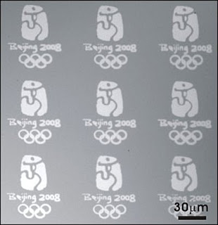
Each Olympic logo is so small — 70 micrometers long and 60 micrometers wide — that 2,500 of them would fit on a grain of rice.
EVANSTON, Ill. --- Northwestern University nanoscientist Chad A. Mirkin has mass-produced the 2008 Summer Olympics logo -- 15,000 times. All the logos take up only one square centimeter of space.

Mirkin and his colleagues printed the logos as well as an integrated gold circuit using a new printing technique, called Polymer Pen Lithography (PPL), that can write on three different length scales using only one device.
The PPL technique, to be published Aug. 15 in Science Express, is a fast, inexpensive and simple way to print on the nanometer, micrometer and millimeter length scales.

The new printing method could find use in computational tools (the electronics that make up these tools), medical diagnostics (gene chips and arrays of biomolecules) and the pharmaceutical industry (arrays for screening drug candidates), among others.

“While watching the Olympics opening night ceremonies I was delighted to see that printing was highlighted as one of ancient China’s four great inventions,” said Mirkin, George B. Rathmann Professor of Chemistry in the Weinberg College of Arts and Sciences, professor of medicine and professor of materials science and engineering. Mirkin led the study.

“We consider Dip-Pen Nanolithography, which is nanotechnology’s version of the quill pen, and now Polymer Pen Lithography to be two of Northwestern’s most important inventions.”

Polymer Pen Lithography uses arrays of tiny pens made of polymers to print over large areas with nanoscopic through macroscopic resolution. By simply changing contact pressure (and the amount the pens deform), as well as the time of delivery, dots of various diameters can be produced. (The pen tips snap back to their original shape when the pressure is removed.)

“We can go, in a sense, from an ultra fine point Sharpie® to one with a fat tip,” said Mirkin, director of Northwestern’s International Institute for Nanotechnology. “The tip of each polymer pen starts with nanometer-scale sharpness, but if we press down harder the tip flattens out. This gives us great flexibility in the structures we can produce.”

In the case of the Olympic logo, the researchers started with a bitmap image of the logo and uniformly printed 15,000 replicas onto a gold substrate using an “ink” of the molecule 16-mercaptohexadecanoic acid. (The ink is a mere one molecule thick.) This took less than 40 minutes.

The logo is so small that 2,500 of them would fit on a single grain of rice. The letters and numbers, “Beijing 2008,” were generated from approximately 20,000 dots that were 90 nanometers in diameter. Then, with more force applied to the pens, the stylized human figure and the Olympic rings were made from approximately 4,000 dots that were 600 nanometers in diameter.

The integrated circuit the researchers built had features on all three length scales, perfectly integrated together. Building the circuit took about two hours. As with the Olympic logo, the structures were made by making multiple printing passes with the same tool (the pen array, which has an ink reservoir).

Polymer Pen Lithography simplifies and takes the best of two existing printing techniques -- the high registration and sub-50-nanometer resolution of Dip-Pen Nanolithography (DPN) and the use of a polymer stamp to transfer a pattern in microcontact printing. (Mirkin invented DPN in 1999.)

The PPL method requires a dot matrix image of the structure to be printed (the Olympic logo, for example) and an atomic force microscope. The researchers have demonstrated arrays with as many as 11 million pens.

The Science paper is titled “Polymer Pen Lithography.” In addition to Mirkin, other authors are Fengwei Huo (lead author), Zijian Zheng, Gengfeng Zheng, Louise R. Giam and Hua Zhang, all of Northwestern.

The research was supported by the Air Force Office of Scientific Research, the Defense Advanced Research Projects Agency and the National Science Foundation.

Contact: Megan Fellman fellman@northwestern.edu 847-491-3115 Northwestern University

Tags: or and

Tuesday, September 16, 2008

Self-assembling polymer arrays improve data storage potential

block copolymers self-assemble into structures

Caption: Researchers from the University of Wisconsin-Madison and Hitachi Global Storage Technologies have reported a way to improve the quality and resolution of patterned templates such as those used to manufacture hard drives and other data storage devices. When added to lithographically patterned surfaces such as those shown in the upper left panel of this composite image, specially designed materials called block copolymers self-assemble into structures, shown in the upper right panel, with improved quality and resolution over the original patterns.

These structures can be used to make templates with nanoscale elements like the silicon pillars shown in the bottom panel, which may be useful for manufacturing higher capacity hard disk drives. Photo by: courtesy Paul Nealey. Date: May/July 2008
MADISON — A new manufacturing approach holds the potential to overcome the technological limitations currently facing the microelectronics and data-storage industries, paving the way to smaller electronic devices and higher-capacity hard drives.

"In the past 20 to 30 years, researchers have been able to shrink the size of devices and the size of the patterns that you need to make those devices, following the use of the same types of lithographic materials, tools and strategies, only getting better and better at it," says Paul Nealey, director of the University of Wisconsin-Madison Nanoscale Science and Engineering Center (NSEC).

Now, those materials and tools are reaching their fundamental technical limits, hampering further performance gains. In addition, Nealey says, extrapolating lithography — a process used to pattern manufacturing templates — to smaller and smaller dimensions may become prohibitively expensive. Further advances will require a new approach that is both commercially viable and capable of meeting the demanding quality-control standards of the industry.
In a collaborative effort between academic and industry, chemical and biological engineering professors Nealey and Juan de Pablo, and other colleagues from the UW-Madison NSEC partnered with researchers from Hitachi Global Storage Technologies to test a promising new twist on the traditional methods. In the Aug. 15 issue of the journal Science, the team demonstrates a patterning technology that may revolutionize the field, offering performance improvements over existing methods even while reducing the time and cost of manufacturing.

The method builds on existing approaches by combining the lithography techniques traditionally used to pattern microelectronics with novel self-assembling materials called block copolymers. When added to a lithographically patterned surface, the copolymers' long molecular chains spontaneously assemble into the designated arrangements.

"There's information encoded in the molecules that results in getting certain size and spacing of features with certain desirable properties," Nealey explains. "Thermodynamic driving forces make the structures more uniform in size and higher density than you can obtain with the traditional materials."

The block copolymers pattern the resulting array down to the molecular level, offering a precision unattainable by traditional lithography-based methods alone and even correcting irregularities in the underlying chemical pattern. Such nanoscale control also allows the researchers to create higher-resolution arrays capable of holding more information than those produced today.

In addition, the self-assembling block copolymers only need one-fourth as much patterning information as traditional materials to form the desired molecular architecture, making the process more efficient, Nealey says. "If you only have to pattern every fourth spot, you can write those patterns at a fraction of the time and expense," he says.

In addition to shared intellectual contributions, the collaboration between the UW-Madison and Hitachi teams provided very clear objectives about creating a technology that is industrially viable. "This research addresses one of the most significant challenges to delivering patterned media — the mass production of patterned disks in high volume, at a reasonable cost," says Richard New, director of research at Hitachi Global Storage Technologies. "The large potential gains in density offered by patterned media make it one of the most promising new technologies on the horizon for future hard disk drives."

In its current form, this method is very well-suited for designing hard drives and other data-storage devices, which need uniformly patterned templates — exactly the types of arrangements the block copolymers form most readily. With additional advances, the approach may also be useful for designing more complex patterns such as microchips.

"These results have profound implications for advancing the performance and capabilities of lithographic materials and processes beyond current limits," Nealey says. ###

In addition to support from the National Science Foundation, NSEC and Hitachi Global Storage Technologies, additional funding was provided by the Semiconductor Research Corporation. — Jill Sakai, (608) 262-9772, jasakai@wisc.edu

Contact: Paul Nealey nealey@engr.wisc.edu 608-265-8171 University of Wisconsin-Madison

Monday, September 15, 2008

Turning waste material into ethanol

Nanoscale Catalysts

Caption: In this transmission electron micrograph of the mesoporous nanospheres, the nano-scale catalyst particles show up as the dark spots. Using particles this small (~ 3 nm) increases the overall surface area of the catalyst by roughly 100 times. Credit: US Department of Energy's Ames Laboratory, Usage Restrictions: None.
Nanoscale catalysts could tap syngas as cheap source of ethanol

AMES, Iowa – Say the word "biofuels" and most people think of grain ethanol and biodiesel. But there's another, older technology called gasification that's getting a new look from researchers at the U.S. Department of Energy's Ames Laboratory and Iowa State University. By combining gasification with high-tech nanoscale porous catalysts, they hope to create ethanol from a wide range of biomass, including distiller's grain left over from ethanol production, corn stover from the field, grass, wood pulp, animal waste, and garbage.
Gasification is a process that turns carbon-based feedstocks under high temperature and pressure in an oxygen-controlled atmosphere into synthesis gas, or syngas. Syngas is made up primarily of carbon monoxide and hydrogen (more than 85 percent by volume) and smaller quantities of carbon dioxide and methane.

It's basically the same technique that was used to extract the gas from coal that fueled gas light fixtures prior to the advent of the electric light bulb. The advantage of gasification compared to fermentation technologies is that it can be used in a variety of applications, including process heat, electric power generation, and synthesis of commodity chemicals and fuels.

"There was some interest in converting syngas into ethanol during the first oil crisis back in the 70s," said Ames Lab chemist and Chemical and Biological Science Program Director Victor Lin. "The problem was that catalysis technology at that time didn't allow selectivity in the byproducts. They could produce ethanol, but you'd also get methane, aldehydes and a number of other undesirable products."

A catalyst is a material that facilitates and speeds up a chemical reaction without chemically changing the catalyst itself. In studying the chemical reactions in syngas conversion, Lin found that the carbon monoxide molecules that yielded ethanol could be "activated" in the presence of a catalyst with a unique structural feature.

"If we can increase this 'activated' CO adsorption on the surface of the catalyst, it improves the opportunity for the formation of ethanol molecules," Lin said. "And if we can increase the amount of surface area for the catalyst, we can increase the amount of ethanol produced."

Lin's group looked at using a metal alloy as the catalyst. To increase the surface area, they used nano-scale catalyst particles dispersed widely within the structure of mesoporous nanospheres, tiny sponge-like balls with thousands of channels running through them. The total surface area of these dispersed catalyst nanoparticles is roughly 100 times greater than the surface area you'd get with the same quantity of catalyst material in larger, macro-scale particles.

It is also important to control the chemical makeup of the syngas. Researchers at ISU's Center for Sustainable Environmental Technologies , or CSET, have spent several years developing fluidized bed gasifiers to provide reliable operation and high-quality syngas for applications ranging from replacing natural gas in grain ethanol plants to providing hydrogen for fuel cells.

"Gasification to ethanol has received increasing attention as an attractive approach to reaching the Federal Renewable Fuel Standard of 36 billion gallons of biofuel," said Robert Brown, CSET director.

"The great thing about using syngas to produce ethanol is that it expands the kinds of materials that can be converted into fuels," Lin said. "You can use the waste product from the distilling process or any number of other sources of biomass, such as switchgrass or wood pulp. Basically any carbon-based material can be converted into syngas. And once we have syngas, we can turn that into ethanol." ###

The research is funded by the DOE's Offices of Basic Energy Sciences and Energy Efficiency and Renewable Energy.

Ames Laboratory is a U.S. Department of Energy Office of Science laboratory operated for the DOE by Iowa State University. The Lab conducts research into various areas of national concern, including the synthesis and study of new materials, energy resources, high-speed computer design, and environmental cleanup and restoration.

Contact: Kerry Gibson kgibson@ameslab.gov 515-294-1405 DOE/Ames Laboratory

Tags: or and