Friday, November 30, 2007

Developing kryptonite for Superbug

methicillin resistant Staphylococcus aureus (MRSA) bacteriaUniversity of Idaho scientists' nanoelectronics, nanomaterials, and Staphylococcus aureus research efforts generate new MRSA detection and treatment strategies

MOSCOW/POST FALLS, Idaho – University of Idaho researchers are crossing academic and geographical bounds to develop more effective defenses against Staphylococcus aureus bacteria and other deadly pathogens.
One of the goals of that effort is to create much faster and more accurate identification of strains resistant to the antibiotic methicillin, formally known as methicillin-resistant Staphylococcus aureus, or MRSA.

Breakthrough detection technologies are already in hand in University of Idaho labs. Nanoelectronic biosensors at the university’s Center for Advanced Microelectronics and Biomolecular Research (CAMBR) recently have cut detection time for staph from the industry standard of up to three days down to three hours.

Researchers now are focused on tweaking the device so that it can provide a complete toxin profile of staph that will quickly reveal the virulence of infections. To accomplish that goal, researchers from the university’s Center of Biomedical Research Excellence (COBRE) are partnering with CAMBR scientists.

Eventually, it is hoped that even the hard-to-identify MRSA bacteria will be detected quickly using some iteration of the nanotechnology.

MRSA’s resistance to antibiotics has earned it “superbug” status. It is responsible for more 94,000 infections and 16,000 deaths annually in the U.S. alone, according to recent Center for Disease Control reports. Those numbers indicate it is a greater health threat to Americans than the AIDS virus.

The spiking MRSA death toll recently reported by the Center for Disease Control presents formidable motivation to move infectious disease research ahead, and to get life saving nanotechnologies into the marketplace. University of Idaho scientists are focused on both goals.

The CAMBR Biosensor The vast majority of hospitals, including all regional facilities in Coeur d’Alene, Idaho, and Spokane, Wash., still culture staph in Petri dishes. The culture usually takes one to two days to mature until it is identifiable. CAMBR biosensors identify staph within three hours, with an equally astounding increase in accuracy. The device already has successfully detected the staphylococcus aureus 16S rRNA gene, 16S rRNA, and enterotoxin B, as well as a biomark for lung cancer.

“Our electronic detection capability is approximately 1,000 times more sensitive than the chemilumine technologies currently being used in clinical laboratories,” said Wusi Maki, principal investigator for CAMBR biomolecular research.

“Our plan is to work with Professor Greg Bohach and use the nanosensor CAMBR has developed to provide a toxin profile that will tell us very quickly, and very accurately, if we are looking at lethal or just mild staph,” said Maki.

Bohach is principal investigator and director of the COBRE in the university’s Department of Microbiology, Molecular Biology and Biochemistry (MMBB).

There currently is no method available to quickly and accurately judge the virulence of staph bacteria, Bohach noted.

Finding effective “capture molecules,” those that adhere specifically to staph and its toxins, is key to creating a biosensor-generated toxin profile and insights into the virulence of specific staph infections.

Finding an RNA Fragment in a Molecular Library Stack University of Idaho MMBB graduate student Ryan Dobler has been working with Bohach and scientists at CAMBR labs to identify and replicate capture molecules. Specifically, he has been searching through a vast molecular library looking for an aptamer molecule, “a piece of RNA that binds to a target,” Dobler explained.

His work has confirmed that the large pool of RNA fragments he studied are binding; specifically, that they attach to fibronectin binding protein. “Fibronectin binding protein is a unique protein that’s found on the surface of staph bacteria,” Dobler said. “It helps bind the staph to human tissue.”

The research has not yet yielded an aptamer that would most effectively and most specifically recognize staph. In his year-long investigation, Dobler tested about 80 samples among the thousands that may yield results.

He is writing up his research, and will present his findings in his master’s thesis in December. Bohach, Maki and their teams hope to find funding to continue the study.

“A good example of capture molecules are those that attach themselves to the toxins that staph makes,” Bohach explained. “We hope to identify particularly those toxins that are associated with the more virulent strains, including MRSA strains. There’s quite a bit known about the toxins, and we can – in a limited number of steps – screen and isolate staph for many different toxins at the same time.”

“So if you’re looking specifically for MRSA, you could look for those bacterial molecules that are associated with it, and through that unique association, identify it with precision,” he said.

As the research progresses, capture molecules for a variety of identifying toxins will be incorporated onto the biosensor, which will quickly read and accurately translate the toxin profile.

Using staph Pathogenesis as a Treatment Delivery System

Bohach and others members of his team also are looking at the mechanisms staph bacteria employ to enter host cells and proliferate.

Using nanowires and other nanomaterials (NMs), they aim to hijack the methods bacteria use for toxin delivery, and use them to deliver drug therapies specifically to infected cells.

Bohach is working with University of Idaho professor of physics and materials engineer David McIlroy, microbiologist Carolyn Hovde and others to develop nanowires and other nanomaterials (NMs) for use as innovative drug delivery systems.

McIlroy leads a team of seven researchers supported by the university’s Blue Ribbon Strategic Initiative funding. Their goal is to integrate nanonmaterials research with cell biology and bioscience research.

The Idaho researchers have found that NMs penetrate tumors easily, and can do so coated with antibodies or other materials that seek and destroy infected cells, while sparing normal cells.

They are looking for ways to enable NMs to more readily penetrate the targeted cells, and they report that nanowires coated with the protein fibronectin penetrate cells more easily than uncoated nanowires. In experiments with human and animal cells, they have illustrated that coated nanowires can enter and deliver a toxic agent (StxA1) that kills the cells.

Microbiologists Bohach and Hovde work with CAMBR scientists including: Maki, biochemist; Shiva Restage, organic chemist; Miramar Mishap, surface chemist and nanofabrication expert; and Brian Filanoski, a biochemist studying optical detection of bio-agents.

University of Idaho CAMBR biosensor breakthroughs have recently generated two patent applications. The technology is at the demonstration phase and work is needed to bring it to a marketable system, said Maki. “All the building blocks are in place to produce a real system. With the right investment and focus, the technology could be made ready by the teams in Post Falls and Moscow in a few years," she said.

The technology developers have experience delivering commercial technologies, and that task is within the charter of the CAMBR organization, she added.

Once developed and adopted for use in hospitals, biosensors would impact both those who test positive and those who test negative for the bacteria. For the duration of the current one to three day wait for a staph culture, hospitals must isolate the patient. Insurance seldom covers that expense, so patients and hospitals currently pick up the hefty tab.

“There is an immediate need for faster, more accurate staph detection,” said Maki. “Quick identification in hospitals could save many lives, and millions of dollars.”

###

About the University of Idaho

Founded in 1889, the University of Idaho is the state’s flagship higher-education institution and its principal graduate education and research university, bringing insight and innovation to the state, the nation and the world. University researchers attract nearly $100 million in research grants and contracts each year; the University of Idaho is the only institution in the state to earn the prestigious Carnegie Foundation ranking for high research activity. The university’s student population includes first-generation college students and ethnically diverse scholars. Offering more than 150 degree options in 10 colleges, the university combines the strengths of a large university with the intimacy of small learning communities. For information, visit www.uidaho.edu.

Additional staph Research and Partnerships:

University of Idaho COBRE co-principal investigator, Mark McGuire, professor of veterinary science, is researching S. aureus’ ability to grow and produce a wide variety of virulence factors, and their roles in the establishment and progression of diseases such as mastitis. Specifically, he is studying glycerol monolaurate (GML) and lauric acid, which have been shown to have inhibitory effects on the production of several virulence factors, and inhibits the growth of staph bacteria.

Washington State University's Larry Fox focuses his research on the microbiology and pathology of clinical mastitis in dairy cows, and toward an increasing management emphasis to reduce its economic impact on farms. Fox has been an active member and leader of the National Mastitis Council and other ADSA and USDA committees.

Bill Davis is the director of the WSU Monoclonal Antibody Center and the Flow Cytometry Facility. The Center’s program in immunology is focused on analysis of the mechanisms regulating the immune response to infectious agents and derived vaccines.

Contact: Joni Kirk joni@uidaho.edu 208-885-7725 University of Idaho

Find the Perfect Fine Art and Image Gifts

Technorati tags: and or and or or Rememberance Hanukkah 5768 and Merry Christmas from Santa Claus and Using Supercomputers To Make Safer Nuclear Reactors

Thursday, November 29, 2007

Using Supercomputers To Make Safer Nuclear Reactors

Rensselaer researcher will lead $3 million DoE study to improve safety of tomorrow’s reactors

Troy, N.Y. — Rensselaer Polytechnic Institute is leading a $3 million research project that will pair two of the world’s most powerful supercomputers to boost the safety and reliability of next-generation nuclear power reactors.
The three-year project, funded by the U.S. Department of Energy, will call upon a diverse team of researchers and institutions to create highly detailed computer models of a new proposed type of nuclear reactor. These models could play a key role for the future development of the new reactors, which meet stringent safety and nonproliferation criteria, can burn long-lived and highly radioactive materials, and can operate over a long time without using new fuel.

Running simulations of such a vast virtual model, where scientists can watch the reactor system perform as a whole or zoom in to focus on the interaction of individual molecules, requires unprecedented computing power. To undertake such a task, researchers will use both Rensselaer’s Computational Center for Nanotechnology Innovations, or CCNI — the world’s seventh most powerful supercomputer — and Brookhaven National Laboratory’s New York Blue — the world’s fifth most powerful supercomputer. body>

The research program, titled “Deployment of a Suite of High Performance Computational Tools for Multiscale Multiphysics Simulation of Generation-IV Reactors,” is unique in scale as well as its geographic concentration. Along with Rensselaer and Brookhaven, the partnership includes researchers from Columbia University and the State University of New York at Stony Brook, all New York state-based institutions. Another Empire State connection is computer giant IBM, headquartered in New York and the maker of Blue Gene supercomputers. The company developed, designed, and built both CCNI and New York Blue.

Rensselaer nuclear engineering and engineering physics professor Michael Podowski, a world-renowned nuclear engineering and multiphase science and technology expert who also heads Rensselaer’s Interdisciplinary Center for Multiphase Research, is project director and principal investigator of the new study.

Podowski said nuclear power should likely gain traction and become more widespread in the coming decades, as nations seek ways to fulfill their growing energy needs without increasing their greenhouse emissions. Nuclear reactors produce no carbon dioxide, Podowski said, which gives this energy source an advantage over coal and other fossil fuels for large-scale electricity production.

The main challenge of nuclear power plants, he said, is that they produce radioactive waste as a byproduct of energy production. But several governments around the world, including the United States, are working tirelessly with universities, research consortia, and the private sector to design and develop new, so-called “fourth generation” nuclear reactors that are safer and produce less waste. These reactors will be necessary in the coming decades as nuclear reactors currently in use reach the end of their life cycle and are gradually decommissioned.

The type of reactor that Podowski’s team will be modeling, a sodium-cooled fast reactor, or SFR, is among the most promising of these next-generation designs. The primary advantage of the SFR is its ability to burn highly radioactive nuclear materials, which today’s reactors cannot do, Podowski said.

Whereas current reactors source their power from uranium, SFRs can also source their power from fuel that is a mixture of uranium and plutonium. In particular, SFRs will be able to burn both weapons-grade plutonium and pre-existing nuclear waste, Podowski said. Thanks to their high temperatures, SFRs will also produce electricity at higher efficiency than current nuclear reactors.

So along with producing less toxic waste, SFRs should be able to actively help reduce the amount of existing radioactive materials by burning already-spent nuclear waste, he said. SFRs also offer a viable, productive way to start getting rid of the world’s stockpile of weapons-grade nuclear fuel.

“The idea is to design reactors that can use this material and that are safe,” Podowski said. “With this project, we are trying to improve the understanding of the physics of the system in order to provide the necessary advancements for the design of new, safer, and better reactors.”

To expedite this understanding, Podowski’s team will construct an incredibly detailed computer model of an SFR. The model will allow researchers to zoom in and watch as individual molecules of fission gas and fuel material interact with other molecules inside the reactor, or zoom out to simulate and test the behavior of the reactor as a whole. Creating such a model, not to mention running hundreds or thousands of simulations with slightly modified models and conditions, requires a tremendous amount of computing power and would not be possible without the help of supercomputers, Podowski said.

In order to construct the model and run these massive simulations, Podowski’s team will develop and deploy a suite of powerful, high-performance software tools capable of performing such a task. Since no one computer code or technology is robust enough to model the wide variety of systems that comprise an SFR, the team will use different computer codes for different parts of the model and then develop new ways of linking those differently coded segments together into a single, cohesive, seamless package.

The researchers will use simulations to study fuel performance, local core degradation, fuel particle transport, and several other aspects of the SFRs. By better understanding how design and operational issues will affect the reactor at different stages in its life cycle, Podowski said, the new study will help to dramatically improve the design and safety of SFRs long before the first physical prototype is ever built.

“Nuclear reactors are safe, but nothing is perfect,” Podowski said. “So the issue is to anticipate what could happen, understand how it could happen, and then take actions to both prevent it from happening and, in the extremely unlikely instance of an accident, be able to mitigate the consequences.”

Podowski will lead a team of more than 10 researchers on the three-year project. Rensselaer associate professor Kenneth Jansen, assistant professor Li Liu, and research assistant professor Steven Antal — all of the Department of Mechanical, Aerospace, and Nuclear Engineering — are listed as co-PIs and will contribute to the study. Podowski said he also expects to hire a postdoctoral researcher and at least three doctoral students to work on the project.

The rest of the team includes James Glimm from Stony Brook University; David Keyes from Columbia University; as well as Lap Cheng and Roman Samulyak from Brookhaven National Laboratory.

About Rensselaer: Rensselaer Polytechnic Institute, founded in 1824, is the nation’s oldest technological university. The university offers bachelor’s, master’s, and doctoral degrees in engineering, the sciences, information technology, architecture, management, and the humanities and social sciences. Institute programs serve undergraduates, graduate students, and working professionals around the world.

Rensselaer faculty are known for pre-eminence in research conducted in a wide range of fields, with particular emphasis in biotechnology, nanotechnology, information technology, and the media arts and technology. The Institute is well known for its success in the transfer of technology from the laboratory to the marketplace so that new discoveries and inventions benefit human life, protect the environment, and strengthen economic development.

Contact: Michael Mullaney mullam@rpi.edu 518-276-6161 Rensselaer Polytechnic Institute

Technorati Tags: or and and or and or Rememberance Hanukkah 5768 and
Vintage Santa Claus
and “Heftier” Atoms Reduce Friction at the Nanoscale

Wednesday, November 28, 2007

“Heftier” Atoms Reduce Friction at the Nanoscale

'Heftier' Atoms Reduce Friction at the NanoscalePHILADELPHIA –- A research team led by a University of Pennsylvania mechanical engineer has discovered that friction between two sliding bodies can be reduced at the molecular, or nanoscale, level by changing the mass of the atoms at the surface. “Heavier” atoms vibrate at a lower frequency, reducing energy lost during sliding.

The study appears in the November issue of the journal Science.

Penn researchers, along with colleagues at the University of Houston and the University of Wisconsin now at IBM’s Zurich Research Laboratory and the Argonne National Laboratory,
used atomic force microscopy like an old-fashioned record needle, sliding it along single-crystal diamond and silicon surfaces to measure the force of friction. Before doing so, researchers coated each crystal surface with one of two adsorbates designed to best exhibit variations in the mass of the atoms at the surface without changing the chemistry. The first adsorbate was a single layer of hydrogen atoms. The second was its chemically similar but heavier cousin, deuterium, a hydrogen atom with a neutron stuffed inside its nucleus.

“Our study found that the larger mass of the terminating atoms at the surface, in this case deuterium, led to less energy lost to heat in the system,” Robert Carpick, associate professor of mechanical engineering and applied mechanics at Penn, said. “The larger atomic mass of deuterium results in a lower natural vibration frequency of the atoms. These atoms collide less frequently with the tip sliding over it, and thus energy is more slowly dissipated away from the contact.”

The single layer of atoms at the surface of each crystal acts as an energy transfer medium, absorbing kinetic energy from the tip of the atomic force microscope. The tips were less than 50nm in radius at their ends. How much energy is absorbed is dependent, researchers found, on the adsorbates’ natural atomic vibration frequencies. The heavier an atom, the lower its vibrational frequency. The lighter an atom, the faster the vibrations and thus the faster the dissipation of energy from the contact in the sample. Keeping the atoms chemically similar avoided any changes arising from chemical bonding.

The Penn findings provide a better understanding of the nature of friction, which lacks a comprehensive model at the fundamental level.

“We know how some properties -- adhesion, roughness and material stiffness for example -- contribute to friction over several length scales, but this work reveals how truly atomic-scale phenomena can and do play a meaningful role,” Matthew Brukman, a contributor to the research, said.

Industry has long been concerned with ways to reduce friction between objects, both to maintain the energy of the system as well as to reduce heat-generation and wear, which can weaken machinery and materials to the breaking point. The authors note that improved friction models can be used for the opposite effect; makers of some mechanical components such as automobile clutches may be interested in techniques to increase friction without changing the wear or adhesion of materials.

Even in the absence of rough edges or wear between sliding bodies, friction between the atoms at the surface causes vibrations which dissipate energy, but the exact mechanisms of this process remain unresolved. Scientists continue to explore the details of friction, and other open questions include the effects of environmental variables such as temperature and atmosphere. ###

The research was performed by Carpick and Brukman of the Department of Materials Science and Engineering in Penn's School of Engineering and Applied Science; Rachel J. Cannara, now of the IBM Zurich Research Laboratory; Anirudha V. Sumant, now at Argonne National Laboratory; and Steven Baldelli and Katherine Cimatu of the University of Houston.

The research was supported by the National Science Foundation, an NSF Graduate Research Fellowship and the Air Force Office of Scientific Research.

Contact: Jordan Reese jreese@upenn.edu 215-573-6604 University of Pennsylvania

Technorati Tags: or and and or and or Rememberance Hanukkah 5768 and Andrew Jackson and Delft University of Technology rotates electron spin with electric field

Tuesday, November 27, 2007

Delft University of Technology rotates electron spin with electric field

electron microscope photo of a nanostructure similar to that used in the experiment.

Caption: An electron microscope photo of a nanostructure similar to that used in the experiment. The light-grey colors show the metal structure (made of gold) used to create an electric trap (white lines) for the electrons. A voltage (V) that changes with time is applied to the rightmost piece of metal. As a result, the electron, which is locked in the right trap, feels an electric field. This electric field causes the electron to move (white dotted line), so that the position of the electron changes with time.

Credit: TU Delft. Usage Restrictions: None
Researchers at the Delft University of Technology’s Kavli Institute of Nanoscience and the Foundation for Fundamental Research on Matter (FOM) have succeeded in controlling the spin of a single electron merely by using electric fields. This clears the way for a much simpler realization of the building blocks of a (future) super-fast quantum computer. The scientists will publish their work in Science Express on Thursday 1 November.

Controlling the spin of a single electron is essential if this spin is to be used as the building block of a future quantum computer. An electron not only has a charge but, because of its spin, also behaves as a tiny magnet. In a magnetic field, the spin can point in the same direction as the field or in the opposite direction, but the laws of quantum mechanics also allow the spin to exist in both states simultaneously. As a result, the spin of an electron is a very promising building block for the yet-to-be-developed quantum computer; a computer that, for certain applications, is far more powerful than a conventional computer.
At first glance it is surprising that the spin can be rotated by an electric field. However, we know from the Theory of Relativity that a moving electron can ‘feel’ an electric field as though it were a magnetic field. Researchers Katja Nowack and Dr. Frank Koppens therefore forced an electron to move through a rapidly-changing electric field. Working in collaboration with Prof. Yuli V. Nazarov, theoretical researcher at the Kavli Institute of Nanoscience Delft, they showed that it was indeed possible to turn the spin of the electron by doing so.

The advantage of controlling spin with electric fields rather than magnetic fields is that the former are easy to generate. It will also be easier to control various spins independently from one another - a requirement for building a quantum computer - using electric fields. The team, led by Dr. Lieven Vandersypen, is now going to apply this technique to a number of electrons. ###

Contact: Frank Nuijens F.W.Nuijens@tudelft.nl 31-152-784-259 Delft University of Technology

Technorati Tags: or and and or and or Rememberance Hanukkah 5768 and Arbeit Macht Frei and Mini-sensor may have biomedical and security applications VIDEO

Monday, November 26, 2007

Mini-sensor may have biomedical and security applications VIDEO

New NIST Mini-Sensor May Have Biomedical and Security Applications

Caption: In NIST's new mini-magnetometer, light from a laser (small gray cylinder at left) passes through a small container (green cube) containing atoms in a gas. The cell and any sample being tested are placed inside a magnetic shield (large grey cylinder). When no sample is present, as in the top image, the atoms' "spins" (depicted inside red circle) align themselves with the laser beam, and the virtually all the light is transmitted through the cell to the detector (blue cube). In the presence of a sample emitting a magnetic field, such as a bomb or a mouse (middle and bottom images), the atoms become more disoriented as the field gets stronger, and less light arrives at the detector. A mouse heart produces a stronger signal than many explosive compounds found, for example, in bombs, if both are located the same distance from the sensor; at greater distances, the detected field is reduced. By monitoring the signal at the detector, scientists can determine the strength of the magnetic field.

Credit: Copyright Loel Barr

Usage Restrictions: Editors: If you use this illustration, you must provide a credit for the artist Loel Barr. The illustration credit should read: © Loel Barr. This illustration may be used without charge for editorial articles that mention the National Institute of Standards and Technology. The copyright on the illustration is retained by Loel Barr.

Ultrasensitive prototype device approaches gold standard for magnetic field detection

A short web-quality video is available in two formats. In the video, John Kitching, an author of the paper, describes his laboratory's work.BOULDER, Colo.- A tiny sensor that can detect magnetic field changes as small as 70 femtoteslas-equivalent to the brain waves of a person daydreaming-has been demonstrated at the National Institute of Standards and Technology (NIST). The sensor could be battery-operated and could reduce the costs of non-invasive biomagnetic measurements such as fetal heart monitoring. The device also may have applications such as homeland security screening for explosives.

Described in the November issue of Nature Photonics,* the prototype device is almost 1000 times more sensitive than NIST's original chip-scale magnetometer demonstrated in 2004 and is based on a different operating principle. Its performance puts it within reach of matching the current gold standard for magnetic sensors, so-called superconducting quantum interference devices or SQUIDs. These devices can sense changes in the 3- to 40-femtotesla range but must be cooled to very low (cryogenic) temperatures, making them much larger, power hungry, and more expensive.

The NIST prototype consists of a single low-power (milliwatt) infrared laser and a rice-grain-sized container with dimensions of 3 by 2 by 1 millimeters. The container holds about 100 billion rubidium atoms in gas form. As the laser beam passes through the atomic vapor, scientists measure the transmitted optical power while varying the strength of a magnetic field applied perpendicular to the beam. The amount of laser light absorbed by the atoms varies predictably with the magnetic field, providing a reference scale for measuring the field. The stronger the magnetic field, the more light is absorbed.

"The small size and high performance of this sensor will open doors to applications that we could previously only dream about," project leader John Kitching says.

The new NIST mini-sensor could reduce the equipment size and costs associated with some non-invasive biomedical tests. (The body's electrical signals that make the heart contract or brain cells fire also simultaneously generate a magnetic field.)
The NIST group and collaborators have used a modified version of the original sensor to detect magnetic signals from a mouse heart.** The new sensor is already powerful enough for fetal heart monitoring; with further work, the sensitivity can likely be improved to a level in the 10 femtotesla range, sufficient for additional applications such as measuring brain activity, the designers say. A femtotesla is one quadrillionth (or a millionth of a billionth) of a tesla, the unit that defines the strength of a magnetic field. For comparison, the Earth's magnetic field is measured in microteslas, and a magnetic resonance imaging (MRI) system operates at several teslas.

To make a complete portable magnetometer, the laser and vapor cell would need to be packaged with miniature optics and a light detector. The vapor cell can be fabricated and assembled on semiconductor wafers using existing techniques for making microelectronics and microelectromechanical systems (MEMS). This design, adapted from a previously developed NIST chip-scale atomic clock, offers the potential for low-cost mass production.

As described in the new paper, NIST scientists demonstrated that the prototype mini-sensor produces a strong signal that changes rapidly with the strength of a magnetic field from the outside world. The device exhibits a consistent minimum level of electromagnetic static, or "white noise," which indicates a stable limit on its overall sensitivity. The authors also estimated that a well-designed compact magnetometer with present sensitivity could operate continuously for weeks on a single AA battery. Magnetometers need to be designed with applications in mind; smaller vapor cells require less power but are also less sensitive. Thus, an application for which low power is critical would benefit from a very small magnetometer, whereas a larger magnetometer would be more suitable for a different application requiring high sensitivity. The NIST work evaluates the tradeoffs between size, power and performance in a quantifiable way.

"This result suggests that millimeter-scale, low-power, inexpensive, femtotesla magnetometers are feasible ... Such an instrument would greatly expand the range of applications in which atomic magnetometers could be used," the paper states.

The NIST device could be used in a heart monitoring technique known as magnetocardiography (MCG), which is sensitive enough to measure fields of few picoteslas emitted by the fetal heart from small currents in heart muscle cells, providing complementary and perhaps better information than an electrocardiogram. With further improvements, the NIST sensor also might be used in magnetoencephalography (MEG), which measures the magnetic fields produced by electrical activity in the brain, helping to pinpoint tumors or determine function of various parts of the brain. The existing mini-sensor likely will be able to detect some brain activity, such as the signals from alpha waves, which are about 1 picotesla in magnitude at a distance of 1 centimeter from the skull surface, but not the fainter signals from the full range of brain function. (Signals of magnitude 1 picotesla are identifiable with a magnetometer sensitivity of 70 femtotesla per root Hertz.) MCG and MEG offer the advantage of not requiring contrast agents or injected tracers as do other medical procedures such as MRI or positron emission tomography (PET).

Potential NIST collaborators are interested in making a portable MEG helmet that could be worn by epileptics to record brain activity before and during seizures. The devices would be much smaller and lighter than the SQUID helmets currently used for such studies. Kitching said the NIST sensor also may have applications in MRI or in airport screening for explosives based on detection of nuclear quadrupole resonance in nitrogen compounds.

As a non-regulatory agency of the Commerce Department, NIST promotes U.S. innovation and industrial competitiveness by advancing measurement science, standards and technology in ways that enhance economic security and improve our quality of life. ###

* Vishal Shah, Svenja Knappe, Peter D.D. Schwindt, and John Kitching. Femtotesla Atomic Magnetometry with a Microfabricated Vapor Cell. Nature Photonics. 1 November 2007.

** Brad Lindseth, Peter Schwindt, John Kitching, David Fischer, Vladimir Shusterman. 2007. Non-contact Measurement of Cardiac Electromagnetic Field in Mice Using an Ultra-small Atomic Magnetometer. Feasibility Study. Presented at Computers in Cardiology, Durham, NC, Sept 30-Oct. 3, 2007.

Background: How the NIST Mini-Sensor Works

The NIST compact magnetometer is based on the so-called SERF (spin-exchange relaxation free) principle, which was used by a group at Princeton University in 2003 to enhance the sensitivity of larger, tabletop-sized magnetometers to outperform SQUIDs. The NIST group developed novel approaches and technologies to adapt the SERF concept for tiny and practical devices.

At zero magnetic field, the atoms' electron "spins" (which can be roughly visualized as tiny magnetic arrows pointing through the electrons) all point in the same direction as the laser beam, and the atoms absorb virtually no light. As the magnetic field is increased, the electrons jump to higher-energy levels and their spins go out of sync, causing the atoms to absorb some of the light.

Ordinarily, the atoms would collide randomly and the electron spins would change direction in between collisions, degrading the sensor signal. The SERF approach maintains consistent spins for a relatively long time (10 milliseconds) by combining a low magnetic field with high temperatures of 150 degrees C (302 degrees F). The spins have little time to adjust in between the collisions. Like cars on a highway, the atoms behave more consistently when conditions are crowded.

Contact: Laura Ost laura.ost@nist.gov 303-497-4880, National Institute of Standards and Technology (NIST) or Presidential Podcast 11/24/07 and Seasons Greetings Horse Drawn Carriage and Make way for the real nanopod

Sunday, November 25, 2007

Let there be light: new magnet design continues magnet lab's tradition of innovation

Caption: Jack Toth, lead lab engineer. Credit: Florida State University. Usage Restrictions: None.TALLAHASSEE, Fla. -- Engineers at Florida State University’s National High Magnetic Field Laboratory have successfully tested a groundbreaking new magnet design that could literally shed new light on nanoscience and semiconductor research.

When the magnet -- called the Split Florida Helix -- is operational in 2010, researchers will have the ability to direct and scatter laser light at a sample not only down the bore, or center, of the magnet, but also from four ports on the sides of the magnet, while still reaching fields above 25 tesla.
By comparison, the highest-field split magnet in the world attains 18 tesla. “Tesla” is a measurement of the strength of a magnetic field; 1 tesla is equal to 20,000 times the Earth’s magnetic field.

Magnetism is a critical component of a surprising number of modern technologies, including MRIs and disk drives, and high-field magnets stand beside lasers and microscopes as essential research tools for probing the mysteries of nature. With this new magnet, scientists will be able to expand the scope of their experimental approach, learning more about the intrinsic properties of materials by shining light on crystals from angles not previously available in such high magnetic fields. In materials research, scientists look at which kinds of light are absorbed or reflected at different crystal angles, giving them insight into the fundamental electronic structure of matter.
The Split Florida Helix design represents a significant accomplishment for the magnet lab’s engineering staff. High magnetic fields exert tremendous forces inside the magnet, and those forces are directed at the small space in the middle . . . that’s where Mag Lab engineers cut big holes in it.Caption: Magnet coil. Credit: Florida State University. Usage Restrictions: None.
“You have enough to worry about with traditional magnets, and then you try to cut huge holes from all four sides from which you can access the magnet,” said lab engineer Jack Toth, who is spearheading the project. “Basically, near the midplane, more than half of the magnet structure is cut away for the access ports, and it’s still supposed to work and make high magnetic fields.”

Magnet engineers worldwide have been trying to solve the problem of creating a magnet with side access at the midsection, but they have met with little success in higher fields. Magnets are created by packing together dense, high-performance copper alloys and running a current through them, so carving out empty space at the heart of a magnet presents a huge engineering challenge.

Instead of fashioning a tiny pinhole to create as little disruption as possible, as other labs have tried, Toth and his team created a design with four big elliptical ports crossing right through the midsection of the magnet. The ports open 50 percent of the total space available for experiments, a capability the laboratory’s visiting scientists have long desired.

“It’s different from any traditional magnet that we’ve ever built before, and even the fabrication of our new parts was very challenging,” Toth said. “In search of a vendor for manufacturing the prototypes, I had phone conversations where people would promise me, ‘Jack, we looked at it from every possible angle and this part is impossible to machine.’”
Of course, that wasn’t the case, and the model coil, crafted from a mix of copper-beryllium blocks and copper-silver plates, met expectations during its testing in a field higher than 32 tesla with no damage to its parts.Caption: Magnet coil. Credit: Florida State University. Usage Restrictions: None.
Though the National Science Foundation-funded model has reached an important milestone, years of work will go into the final product. The lab hopes to have a working magnet for its User Program by 2010, and other research facilities have expressed great interest in having split magnets that can generate high magnetic fields. ###

The National High Magnetic Field Laboratory develops and operates state-of-the-art, high-magnetic-field facilities that faculty and visiting scientists and engineers use for research. The laboratory is sponsored by the National Science Foundation and the state of Florida. To learn more, visit magnet.fsu.edu.

Contact: Jack Toth toth@magnet.fsu.edu 850-644-0854 Florida State University

Technorati Tags: or and and or and or Presidential Podcast 11/24/07 and Seasons Greetings Horse Drawn Carriage and Make way for the real nanopod

Saturday, November 24, 2007

Make way for the real nanopod

Berkeley researchers create first fully-functional nanotube radio

QuickTime video was recorded on the nanotube radio using a Transmission Electron Microscope.This QuickTime video was recorded on the nanotube radio using a Transmission Electron Microscope. At the beginning of the video, the nanotube radio is tuned to a different frequency than that of the transmitted radio signal so the nanotube does not vibrate and only static noise can be heard. As the radio is brought into tune with the transmitted signal, the nanotube begins to vibrate, which blurs its image in the video but allows the music to become audible.
The song is the theme music to Star Wars by John Williams. To see and hear the nanotube radio, click on the image.

BERKELEY, CA -- Make way for the real nanopod and make room in the Guinness World Records. A team of researchers with the U.S. Department of Energy’s Lawrence Berkeley National Laboratory (Berkeley Lab) and the University of California at Berkeley have created the first fully functional radio from a single carbon nanotube, which makes it by several orders of magnitude the smallest radio ever made.

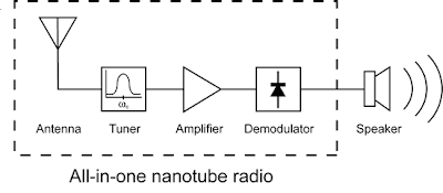
“A single carbon nanotube molecule serves simultaneously as all essential components of a radio -- antenna, tunable band-pass filter, amplifier, and demodulator,” said physicist Alex Zettl, who led the invention of the nanotube radio. “Using carrier waves in the commercially relevant 40-400 MHz range and both frequency and amplitude modulation (FM and AM), we were able to demonstrate successful music and voice reception.”

Given that the nanotube radio essentially assembles itself and can be easily tuned to a desired frequency band after fabrication, Zettl believes that nanoradios will be relatively easy to mass-produce. Potential applications, in addition to incredibly tiny radio receivers, include a new generation of wireless communication devices and monitors. Nanotube radio technology could prove especially valuable for biological and medical applications.

“The entire radio would easily fit inside a living cell, and this small size allows it to safely interact with biological systems,” Zettl said. “One can envision interfaces with brain or muscle functions, or radio-controlled devices moving through the bloodstream.”

It is also possible that the nanotube radio could be implanted in the inner ear as an entirely new and discrete way of transmitting information, or as a radically new method of correcting impaired hearing.

Zettl holds joint appointments with Berkeley Lab's Materials Sciences Division (MSD) and the UC Berkeley Physics Department where he is the director of the Center of Integrated Nanomechanical Systems. In recent years, he and his research group have created an astonishing array of devices out of carbon nanotubes - hollow tubular macromolecules only a few nanometers (billionths of a meter) in diameter and typically less than a micron in length – including sensors, diodes and even a motor. The nanotube radio, however, is the first that – literally – rocks!

“When I was a young kid, I got a transistor radio as a gift and it was the greatest thing I could imagine - music coming from a box I could hold in my hand!” Zettl said. “When we first played our nanoradio, I was just as excited as I was when I first turned on that transistor radio as a kid.”

The carbon nanotube radio consists of an individual carbon nanotube mounted to an electrode in close proximity to a counter-electrode, with a DC voltage source, such as from a battery or a solar cell array, connected to the electrodes for power. The applied DC bias creates a negative electrical charge on the tip of the nanotube, sensitizing it to oscillating electric fields. Both the electrodes and nanotube are contained in vacuum, in a geometrical configuration similar to that of a conventional vacuum tube.

Kenneth Jensen, a graduate student in Zettl’s research group, did the actual design and construction of the radio.
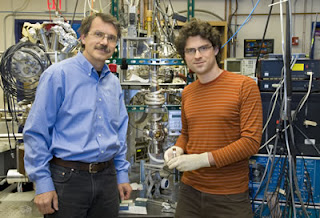
Alex Zettl (left) and his graduate student, Kenneth Jensen.
Alex Zettl (left) and his graduate student, Kenneth Jensen have created the first fully functional radio from a single carbon nanotube, which makes it by several orders of magnitude the world’s smallest radio.
“We started out by making an exceptionally sensitive force sensor,” Jensen said. “Nanotubes are like tiny cat whiskers. Small forces, on the order of attonewtons, cause them to deflect a significant amount. By detecting this deflection, you can infer what force was acting on the nanotube. This incredible sensitivity becomes even greater at the nanotube’s flexural resonance frequency, which falls within the frequencies of radio broadcasts, cell phones and GPS broadcasting. Because of this high resonance frequency, Alex (Zettl) suggested that nanotubes could be used to make a radio.”

Although it has the same essential components, the nanotube radio does not work like a conventional radio. Rather than the entirely electrical operation of a conventional radio, the nanotube radio is in part a mechanical operation, with the nanotube itself serving as both antenna and tuner.

Incoming radio waves interact with the nanotube’s electrically charged tip, causing the nanotube to vibrate. These vibrations are only significant when the frequency of the incoming wave coincides with the nanotube’s flexural resonance frequency, which, like a conventional radio, can be tuned during operation to receive only a pre-selected segment, or channel, of the electromagnetic spectrum.

Amplification and demodulation properties arise from the needle-point geometry of carbon nanotubes, which gives them unique field emission properties. By concentrating the electric field of the DC bias voltage applied across the electrodes, the nanotube radio produces a field-emission current that is sensitive to the nanotube’s mechanical vibrations. Since the field-emission current is generated by the external power source, amplification of the radio signal is possible. Furthermore, since field emission is a non-linear process, it also acts to demodulate an AM or FM radio signal, just like the diode used in traditional radios.

“What we see then is that all four essential components of a radio receiver are compactly and efficiently implemented within the vibrating and field-emitting carbon nanotube,” said Zettl. “This is a totally different approach to making a radio - the exploitation of electro-mechanical movement for multiple functions. In other words, our nanotube radio is a true NEMS (nano-electro-mechanical system) device.”

Because carbon nanotubes are so much smaller than the wavelengths of visible light, they cannot be viewed with even the highest powered optical microscope. Therefore, to observe the critical mechanical motion of their nanotube radio, Zettl and his research team, which in addition to Jensen, also included post-doc Jeff Weldon and graduate student Henry Garcia, mounted their nanotube radio inside a high resolution transmission electron microscope (TEM). A sine-wave carrier radio signal was launched from a nearby transmitting antenna and when the frequencies of the transmitted carrier wave matched the nanotube resonance frequency, radio reception became possible.

“To correlate the mechanical motions of the nanotube to an actual radio receiver operation, we launched an FM radio transmission of the song Good Vibrations by the Beach Boys,” said Zettl. “After being received, filtered, amplified, and demodulated all by the nanotube radio, the emerging signal was further amplified by a current preamplifier, sent to an audio loudspeaker and recorded. The nanotube radio faithfully reproduced the audio signal, and the song was easily recognizable by ear.”

All four essential components of a radio, antenna, tuner, amplifier, and demodulator, may be implemented within a single carbon nanotube.

When the researchers deliberately detuned the nanotube radio from the carrier frequency, mechanical vibrations faded and radio reception was lost. A “lock” on a given radio transmission channel could be maintained for many minutes at a time, and it was not necessary to operate the nanotube radio inside a TEM. Using a slightly different configuration, the researchers successfully transmitted and received signals across a distance of several meters.

“The integration of all the electronic components of a radio happened naturally in the nanotube itself,” said Jensen. “Within a few hours of figuring out that our force sensor was in fact a radio, we were playing music!”

Added Zettl, “Our nanotube radio is sophisticated and elegant in the physics of its operation, but sheer simplicity in technical design. Everything about it works perfectly, without additional patches or tricks.”

Berkeley Lab’s Technology Transfer Department is now seeking industrial partners to further develop and commercialize this technology. ###

A paper on this work is now on-line at the Nano Letters Website. It will also published in the November 2007 print edition of Nano Letters. The paper is entitled “Nanotube Radio” and the co-authors were Zettl, Jensen, Weldon and Garcia. In that same print edition, there appears a paper by Peter Burke and Chris Rutherglen of UC Irvine, reporting on the use of a carbon nanotube as a demodulator.

The nanotube radio research was supported by the U.S. Department of Energy and by the National Science Foundation within the Center of Integrated Nanomechanical Systems.

Berkeley Lab is a U.S. Department of Energy national laboratory located in Berkeley, California. It conducts unclassified scientific research and is managed by the University of California. Visit our Website at lbl.gob/

Additional Information

Contact: Lynn Yarris, lcyarris@lbl.gov, 510-486-5375, DOE/Lawrence Berkeley National Laboratory

Technorati Tags: or and and or and or What will YOU ask the REPUBLICAN presidential candidates? VIDEO and Hanukkah.Dreidel and IH recognizes Clemson nanotechnology for molecule tracking

Friday, November 23, 2007

IH recognizes Clemson nanotechnology for molecule tracking

Illustration of a polymer dot nanoparticle structure. The core is a highly fluorescent polymer semiconductor material.CLEMSON –– The National Institutes of Health has awarded two Clemson chemistry faculty members nearly $1 million to detect, track and image the interior of cells. Jason McNeill and Ken Christensen will receive the $960,000 grant to develop polymer dot nanoparticles for tracking single molecules in live cells.
The development of techniques for following individual molecules within cells is important because scientists could use this technology to determine the body’s defenses against invading viruses and bacteria or how proteins operate within the cell. The technology also could help doctors pinpoint the exact location of cancer cells in order to better focus treatment and minimize damage to healthy tissue. Other possible targets of investigation include plaques and fibrils in the brain associated with Alzheimer's disease and mad cow disease.

For the last decade, scientists around the globe have worked to develop and refine highly fluorescent nanoparticles that light up when bathed with laser light, enabling scientists to pinpoint the location of an individual molecule inside a living cell or tissue.Recently, Clemson chemists developed novel, highly fluorescent nanoparticles called “polymer dots” that can be attached to individual proteins, DNA or invading microbes. According to chemist Jason McNeill, the polymer dot particles are hundreds or thousands of times brighter than conventional fluorescent dyes.
“We were initially interested in developing polymer semiconductor nanoparticles for making inexpensive, highly efficient solar cells and light-emitting displays. When we aimed a laser at the particles in a microscope, we were surprised to see individual particles light up very brightly,” said McNeill.Tissue cells that protect from infection loaded with nanoparticles.
“When I heard about these extremely bright particles, my group was very interested in working with Dr. McNeill to push this technology into live cell imaging,” said Christensen. “Biology is often driven by new discoveries in chemistry and physics and these polymer dots will definitely impact our studies of cellular biology.”

The two chemists credit the highly collaborative, multidisciplinary environment at Clemson as a key factor in this new frontier in nanotechnology.

Details of the nanoparticle technology were recently presented at the 2007 national meeting of the American Chemical Society in Boston and have been published in the Journal of the American Chemical Society, Langmuir and in the Journal of Physical Chemistry. END

Editors: This material is based upon work supported by the NSF/EPSCoR under grant numbers 2001RII-EPS-0132573 and 2004RII-EPS-0447660, NSF CAREER grant number CHE-0547846 and NIH grant number 1R01GM081040. Any opinions, findings and conclusions or recommendations expressed in this material are those of the authors and do not necessarily reflect the views of the National Science Foundation or the National Institutes of Health.

Contact: Jason McNeill, mcneill@clemson.edu, 864-656-4065, WRITER: Susan Polowczuk, (864) 656-2063, spolowc@clemson.edu, Clemson University

Technorati Tags: or and and or and or Rudy Giuliani campaign ad “Challenges” VIDEO and Swearing in of Lyndon B. Johnson as President on Air Force One and Research goes nano, natural and green

Thursday, November 22, 2007

Research goes nano, natural and green

Using only soybeans and water, scientists discover a clean process for making nanoparticles.

In 2002, U.S. farmers harvested 2.7 billion bushels of soybeans. Last year in Missouri, farmers harvested 194 million bushels of soybeans worth about $1.2 billion. Now, a team of researchers at the University of Missouri-Columbia is turning those soybeans into gold, with nothing more than a little water.

MU researcher Kattesh KattiMU researchers Kattesh Katti, Raghuraman Kannan, and Kavita Katti led a team of scientists that have discovered how to make gold nanoparticles using gold salts, soybeans and water. No other chemicals are used in the process, which means this new process could have major environmental implications for the future.
"Typically, a producer must use a variety of synthetic or man-made chemicals to produce gold nanoparticles," said Katti, professor of radiology (School of Medicine) and physics (College of Arts and Science), senior research scientist at MURR, and director of the University of Missouri Cancer Nanotechnology Platform. "In addition, to make the chemicals necessary for production, you need to have other artificial chemicals produced, creating an even larger, negative environmental impact. Our new process only takes what nature has made available to us and uses that to produce a technology that has already proven to have far-reaching impacts in technology and medicine."

Gold nanoparticles are tiny pieces of gold, so small that they cannot be seen by the naked eye. Researchers believe that gold nanoparticles will be used in cancer detection and treatment and in the production of "smart" electronic devices in the computer and telecommunications industry. While the nanotechnology industry is expected to produce large quantities of nanoparticles in the near future, researchers have been worried about the environmental impact of the global nanotechnological revolution.

Since a variety of synthetic chemicals are needed to complete the formation of the gold nanoparticles, the MU research team turned to Mother Nature for assistance. They found that by submersing gold salts in water and then adding soybeans, gold nanoparticles were generated. The water pulls a phytochemical(s) out of the soybean that is effective in reducing the gold to nanoparticles. A second phytochemical(s) from the soybean, also pulled out by the water, then interacts with the nanoparticles to stabilize them and keep them from fusing with the particles nearby. This process creates nanoparticles that are uniform in size in a 100 percent green process.

"This fits with what we need to do for the future," said Kannon, assistant professor of radiology. "We are solving a pollution problem at the very beginning stages of a developing technology. We don't anticipate any waste or byproducts from this new process that would not be biodegradable. Every one of these compounds involved in the process already exists in nature."

The new discovery has created a very large positive response in the scientific community. Researchers from as far away as Germany have been commenting on the discovery's importance and the impact it will have in the future.

"Soy is grown worldwide and Dr. Katti's Nobel Prize winning discovery will ensure that gold nanoparticles-based Nanomedicine products would be made available even to the less developed regions of the world," said B. R. Barwale, 1998 winner of the world food prize and founder of Maharashtra Hybrid Seeds Company in India.

"Dr. Katti's discovery sets up the beginning of a new knowledge frontier that interfaces plant science, chemistry and nanotechnology," said Herbert W. Roesky, a professor and world renowned chemist from the University of Goettingen in Germany.

Katti, Kannan, Henry White, MU professor of physics, and Kavita Katti, a senior research chemist, have filed a patent for the new process and developed a new company, Greennano Company, which focuses on development, commercialization and world wide supply of green nanoparticles for medical and technological applications.

The research team includes Kattesh and Kavita Katti, Kannan, postdoctoral scientists Satish Nune and Nripen Chanda, and graduate student Swapna Mekapothula. The research was funded by grants from the National Cancer Institute. Katti recently presented the work at the annual National Cancer Institute Alliance for Nanotechnology in Cancer Investigator's meeting in October. He also will be presenting the research at the Fourth International Congress of Nanotechnology and the Clean Tech World Congress held in San Francisco in early November.

"Dr. Katti's novel methodology to develop gold nanoparticles with soy will have important implications as the field of nanotechnology blossoms and has greater needs for 'green' synthesis of gold based nanoparticles. It is a very important first step," said Sam Gambhir, director of the Center for Cancer Nanotechnology Excellence at Stanford University.

The discovery also could open doors for additional medical fields, as some of the chemicals used to make nanoparticles are toxic to humans. Having a 100 percent natural process could allow medical researchers to expand the use of the nanoparticles.

"Dr. Katti's discovery of green and non-toxic gold nanoparticles is a significant step to help alleviate the pain and suffering of patients with Pseudoxanthoma elasticum (PXE)," said Frances Bernham, president of the National Association of Pseudoxanthoma elasticum. PXE causes changes in the retina of the eye that results in significant loss of central vision.

"The application of soy for the production of gold nanoparticles is amazing," said Puspendu Das, physical chemistry professor at the Indian Institute of Science Bangalore. "It shows for the first time that chemicals within soy are capable of producing gold nanoparticles. This clearly marks the beginning of a new field of 'Phytochemical-Nanoscience' and opens up a new pathway for discoveries in nanotechnology. This invention will have far-reaching implications in nanoscience and technology research globally since nanoparticles of gold are used in almost every sensor design and are implicated in life sciences for diagnostic and therapeutic applications."

LINKS:Contact: Christian Basi, BasiC@missouri.edu, 573-882-4430, University of Missouri-Columbia

Technorati Tags: or and and or and or John D. Negroponte Remarks on Pakistan VIDEO PODCAST and The Annual Pardoning of the Thanksgiving Turkey and Rice University expert calls for coordination in nanotechnology research

Wednesday, November 21, 2007

Rice University expert calls for coordination in nanotechnology research

Rice chemist Vicki ColvinIn House testimony, Vicki Colvin says nano community needs 'research harmonization'

Nanotechnology holds great promise for the future of cancer therapy and water treatment, but concerns about the safety of nanoproducts may limit these important technological developments, Vicki Colvin said today in comments to the U.S. House Committee on Science and Technology.
Colvin, director of Rice's Center for Biological and Environmental Nanotechnology (CBEN) and executive director of the International Council on Nanotechnology (ICON), was an expert witness at the hearing "Research on Environmental and Safety Impacts of Nanotechnology." The hearing relates to the current direction of the National Nanotechnology Initiative (NNI).

Colvin told the committee she was providing her individual opinions, which have been informed by ICON's work with diverse international stakeholders on nanotechnology research needs in the areas of environment, health and safety (EHS).

ICON, which is affiliated with CBEN, is an international organization with members from academia, nongovernmental organizations, industry and government dedicated to the safe, responsible and beneficial development of nanotechnology. ICON's EHS database is the first to integrate the diverse scientific literature on the impacts of nanoparticles

She called on the National Nanotechnology Initiative to release a detailed strategy for nano-EHS research no later than fall 2008.

"Going from a climate of uncertainty to one of confidence in managing nanotechnology risk is a massive undertaking that will take years to fully develop," Colvin said. "It will also take careful planning and coordination among agencies in this government and abroad. The ultimate plan would be most effectively organized by two, maybe three, overarching outcomes that stakeholders agree will give us more confidence in managing risks."

Colvin emphasized the importance of unifying "researchers' languages, methods and materials," which she referred to as "research harmonization" tools.

"If you fund five teams to help understand nanotube toxicity and they get five different answers, you are actually worse off because your research creates uncertainty rather than combat it," she said.

Colvin said there is a real need for government intervention.

"If left to ourselves, we might harmonize as a community in five to 10 years -- too long to wait for nanotechnology's innovation. The good news is that the U.S. government can, if it is thoughtful about the mechanisms, help researchers fix this problem quickly and for relatively low cost." ###

To read the full text of Colvin's remarks, visit icon.rice.edu. To interview Colvin about her testimony, contact David Ruth at 713-348-6327 or druth@rice.edu.

Contact: David Ruth druth@rice.edu 713-348-6327 Rice University

Technorati Tags: or and and or and or President Bush Pardons Turkeys "May and Flower" VIDEO PODCAST and Prehistoric Animals Dinosaurs Stegosaurus and Using nanotech to make Robocops

Tuesday, November 20, 2007

Using nanotech to make Robocops

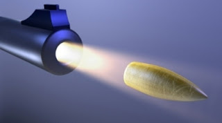
Repelling the force of bulletsBulletproof jackets do not turn security guards, police officers and armed forces into Robocops, repelling the force of bullets in their stride.
New research in carbon nanotechnology however could give those in the line of fire materials which can bounce bullets without a trace of damage.

A research paper published in the Institute of Physics’ Nanotechnology details how engineers from the Centre for Advanced Materials Technology at the University of Sydney have found a way to use the elasticity of carbon nanotubes to not only stop bullets penetrating material but actually rebound their force.

Most anti-ballistic materials, like bullet-proof jackets and explosion-proof blankets, are currently made of multiple layers of Kevlar, Twaron or Dyneema fibres which stop bullets from penetrating by spreading the bullet’s force. Targets can still be left suffering blunt force trauma - perhaps severe bruising or, worse, damage to critical organs.

The elasticity of carbon nanotubes means that blunt force trauma may be avoided and that’s why the engineers in Sydney have undertaken experiments to find the optimum point of elasticity for the most effective bullet-bouncing gear.

Prof Liangchi Zhang and Dr Kausala Mylvaganam from the Centre for Advanced Materials Technology in Sydney, said, “By investigating the force-repelling properties of carbon nanotubes and concluding on an optimum design, we may produce far more effective bulletproof materials.

“The dynamic properties of the materials we have found means that a bullet can be repelled with minimum or no damage to the wearer of a bullet proof vest.”

Working at the scale of a nanometre (one billionth of a metre), condensed matter physicists engineer structures that manipulate individual atomic and molecular interactions. Working at this microscopic scale allows engineers to design fundamentally different and useful materials.

One of these materials is nanotubes, a one-atom thick sheet of graphite, rolled into a cylinder that is held together by a very strong chemical bond called orbital hybridisation.

Nanotubes bind together into a strong ‘rope’ because of the Van der Waals force they share. Van der Waals is the weak attraction that molecules have for one another when they are brought close together, used, for example, by geckos when they stick to a ceiling. ###

Contact: Joseph Winters, joseph.winters@iop.org, 44-020-747-04815, Institute of Physics

Technorati Tags: or and and or and or Mike Huckabee TV Ad Featuring Chuck Norris VIDEO and Prehistoric Animals Dinosaurs Alamosaurus and Wireless sensors to monitor bearings in jet engines

Monday, November 19, 2007

Wireless sensors to monitor bearings in jet engines

Caption: Dimitrios Peroulis, an assistant professor of electrical and computer engineering at Purdue, holds a new MEMS sensor at an Purdue creating wireless sensors to monitor bearings in jet engines

WEST LAFAYETTE, Ind. - Researchers at Purdue University, working with the U.S. Air Force, have developed tiny wireless sensors resilient enough to survive the harsh conditions inside jet engines to detect when critical bearings are close to failing and prevent breakdowns.

The devices are an example of an emerging technology known as "micro electromechanical systems," or MEMS, which are machines that combine electronic and mechanical components on a microscopic scale.
"The MEMS technology is critical because it needs to be small enough that it doesn't interfere with the performance of the bearing itself," said Farshid Sadeghi, a professor of mechanical engineering. "And the other issue is that it needs to be able to withstand extreme heat."

The engine bearings must function amid temperatures of about 300 degrees Celsius, or 572 degrees Fahrenheit.

The researchers have shown that the new sensors can detect impending temperature-induced bearing failure significantly earlier than conventional sensors.

"This kind of advance warning is critical so that you can shut down the engine before it fails," said Dimitrios Peroulis, an assistant professor of electrical and computer engineering.

Findings will be detailed in a research paper to be presented on Tuesday (Oct. 30) during the IEEE Sensors 2007 conference in Atlanta, sponsored by the Institute of Electrical and Electronics Engineers. The paper was written by electrical and computer engineering graduate student Andrew Kovacs, Peroulis and Sadeghi.

The sensors could be in use in a few years in military aircraft such as fighter jets and helicopters. The technology also has potential applications in commercial products, including aircraft and cars.

"Anything that has an engine could benefit through MEMS sensors by keeping track of vital bearings," Peroulis said. "This is going to be the first time that a MEMS component will be made to work in such a harsh environment. It is high temperature, messy, oil is everywhere, and you have high rotational speeds, which subject hardware to extreme stresses."

The work is an extension of Sadeghi's previous research aimed at developing electronic sensors to measure the temperature inside critical bearings in communications satellites.

"This is a major issue for aerospace applications, including bearings in satellite attitude control wheels to keep the satellites in position," Sadeghi said.

The wheels are supported by two bearings. If mission controllers knew the bearings were going bad on a specific unit, they could turn it off and switch to a backup.

"What happens, however, is that you don't get any indication of a bearing's imminent failure, and all of a sudden the gyro stops, causing the satellite to shoot out of orbit," Sadeghi said. "It can take a lot of effort and fuel to try to bring it back to the proper orbit, and many times these efforts fail."

The Purdue researchers received a grant from the U.S. Air Force in 2006 to extend the work for high-temperature applications in jet engines.

"Current sensor technology can withstand temperatures of up to about 210 degrees Celsius, and the military wants to extend that to about 300 degrees Celsius," Sadeghi said. "At the same time, we will need to further miniaturize the size."

The new MEMS sensors provide early detection of impending failure by directly monitoring the temperature of engine bearings, whereas conventional sensors work indirectly by monitoring the temperature of engine oil, yielding less specific data.

The MEMS devices will not require batteries and will transmit temperature data wirelessly.

"This type of system uses a method we call telemetry because the devices transmit signals without wires, and we power the circuitry remotely, eliminating the need for batteries, which do not perform well in high temperatures," Peroulis said.

Power will be provided using a technique called inductive coupling, which uses coils of wire to generate current.

"The major innovation will be the miniaturization and design of the MEMS device, allowing us to install it without disturbing the bearing itself," Peroulis said.

Data from the onboard devices will not only indicate whether a bearing is about to fail but also how long it is likely to last before it fails, Peroulis said. ###

The research is based at the Birck Nanotechnology Center in Purdue's Discovery Park and at Sadeghi's mechanical engineering laboratory.

Writer: Emil Venere, (765) 494-4709, venere@purdue.edu, Sources: Farshid Sadeghi, (765) 494-5719, sadeghi@ecn.purdue.edu, Dimitrios Peroulis, 765 494-3491, dperouli@purdue.edu, Contact: Emil Venere venere@purdue.edu, 765-494-4709 ,Purdue University

Related Web sites:PHOTO CAPTION: Dimitrios Peroulis, an assistant professor of electrical and computer engineering at Purdue, holds a new MEMS sensor at an "environmentally controlled probe station." The wireless sensors are being developed to detect impending bearing failure in jet engines. The probe station recreates extreme conditions inside engines, enabling researchers to test the sensors. (Purdue News Service photo/David Umberger)

Technorati Tags: or and and or and or Google meets Sherlock Holmes and The Life and Adventures of Santa Claus and World's most complex silicon phased-array chip developed at UC-San Diego